EP1470580B1 - Method for bilayer HDP CVD / PE CVD cap in advanced BEOL interconnect structures - Google Patents
Method for bilayer HDP CVD / PE CVD cap in advanced BEOL interconnect structures Download PDFInfo
- Publication number
- EP1470580B1 EP1470580B1 EP02784578A EP02784578A EP1470580B1 EP 1470580 B1 EP1470580 B1 EP 1470580B1 EP 02784578 A EP02784578 A EP 02784578A EP 02784578 A EP02784578 A EP 02784578A EP 1470580 B1 EP1470580 B1 EP 1470580B1
- Authority
- EP
- European Patent Office
- Prior art keywords
- layer
- atomic
- cvd
- silicon
- cap
- Prior art date
- Legal status (The legal status is an assumption and is not a legal conclusion. Google has not performed a legal analysis and makes no representation as to the accuracy of the status listed.)
- Expired - Lifetime
Links
Images




Classifications
-
- H—ELECTRICITY
- H10—SEMICONDUCTOR DEVICES; ELECTRIC SOLID-STATE DEVICES NOT OTHERWISE PROVIDED FOR
- H10W—GENERIC PACKAGES, INTERCONNECTIONS, CONNECTORS OR OTHER CONSTRUCTIONAL DETAILS OF DEVICES COVERED BY CLASS H10
- H10W20/00—Interconnections in chips, wafers or substrates
- H10W20/01—Manufacture or treatment
-
- H—ELECTRICITY
- H10—SEMICONDUCTOR DEVICES; ELECTRIC SOLID-STATE DEVICES NOT OTHERWISE PROVIDED FOR
- H10W—GENERIC PACKAGES, INTERCONNECTIONS, CONNECTORS OR OTHER CONSTRUCTIONAL DETAILS OF DEVICES COVERED BY CLASS H10
- H10W20/00—Interconnections in chips, wafers or substrates
- H10W20/01—Manufacture or treatment
- H10W20/071—Manufacture or treatment of dielectric parts thereof
- H10W20/074—Manufacture or treatment of dielectric parts thereof of dielectric parts comprising thin functional dielectric layers, e.g. dielectric etch-stop, barrier, capping or liner layers
- H10W20/077—Manufacture or treatment of dielectric parts thereof of dielectric parts comprising thin functional dielectric layers, e.g. dielectric etch-stop, barrier, capping or liner layers on sidewalls or on top surfaces of conductors
-
- H—ELECTRICITY
- H10—SEMICONDUCTOR DEVICES; ELECTRIC SOLID-STATE DEVICES NOT OTHERWISE PROVIDED FOR
- H10W—GENERIC PACKAGES, INTERCONNECTIONS, CONNECTORS OR OTHER CONSTRUCTIONAL DETAILS OF DEVICES COVERED BY CLASS H10
- H10W20/00—Interconnections in chips, wafers or substrates
- H10W20/01—Manufacture or treatment
- H10W20/071—Manufacture or treatment of dielectric parts thereof
-
- H—ELECTRICITY
- H10—SEMICONDUCTOR DEVICES; ELECTRIC SOLID-STATE DEVICES NOT OTHERWISE PROVIDED FOR
- H10W—GENERIC PACKAGES, INTERCONNECTIONS, CONNECTORS OR OTHER CONSTRUCTIONAL DETAILS OF DEVICES COVERED BY CLASS H10
- H10W20/00—Interconnections in chips, wafers or substrates
- H10W20/01—Manufacture or treatment
- H10W20/071—Manufacture or treatment of dielectric parts thereof
- H10W20/074—Manufacture or treatment of dielectric parts thereof of dielectric parts comprising thin functional dielectric layers, e.g. dielectric etch-stop, barrier, capping or liner layers
- H10W20/075—Manufacture or treatment of dielectric parts thereof of dielectric parts comprising thin functional dielectric layers, e.g. dielectric etch-stop, barrier, capping or liner layers of multilayered thin functional dielectric layers
-
- H—ELECTRICITY
- H10—SEMICONDUCTOR DEVICES; ELECTRIC SOLID-STATE DEVICES NOT OTHERWISE PROVIDED FOR
- H10W—GENERIC PACKAGES, INTERCONNECTIONS, CONNECTORS OR OTHER CONSTRUCTIONAL DETAILS OF DEVICES COVERED BY CLASS H10
- H10W20/00—Interconnections in chips, wafers or substrates
- H10W20/01—Manufacture or treatment
- H10W20/071—Manufacture or treatment of dielectric parts thereof
- H10W20/081—Manufacture or treatment of dielectric parts thereof by forming openings in the dielectric parts
- H10W20/084—Manufacture or treatment of dielectric parts thereof by forming openings in the dielectric parts for dual-damascene structures
-
- H—ELECTRICITY
- H10—SEMICONDUCTOR DEVICES; ELECTRIC SOLID-STATE DEVICES NOT OTHERWISE PROVIDED FOR
- H10W—GENERIC PACKAGES, INTERCONNECTIONS, CONNECTORS OR OTHER CONSTRUCTIONAL DETAILS OF DEVICES COVERED BY CLASS H10
- H10W20/00—Interconnections in chips, wafers or substrates
- H10W20/40—Interconnections external to wafers or substrates, e.g. back-end-of-line [BEOL] metallisations or vias connecting to gate electrodes
- H10W20/45—Interconnections external to wafers or substrates, e.g. back-end-of-line [BEOL] metallisations or vias connecting to gate electrodes characterised by their insulating parts
- H10W20/47—Interconnections external to wafers or substrates, e.g. back-end-of-line [BEOL] metallisations or vias connecting to gate electrodes characterised by their insulating parts comprising two or more dielectric layers having different properties, e.g. different dielectric constants
-
- H—ELECTRICITY
- H10—SEMICONDUCTOR DEVICES; ELECTRIC SOLID-STATE DEVICES NOT OTHERWISE PROVIDED FOR
- H10W—GENERIC PACKAGES, INTERCONNECTIONS, CONNECTORS OR OTHER CONSTRUCTIONAL DETAILS OF DEVICES COVERED BY CLASS H10
- H10W20/00—Interconnections in chips, wafers or substrates
- H10W20/40—Interconnections external to wafers or substrates, e.g. back-end-of-line [BEOL] metallisations or vias connecting to gate electrodes
- H10W20/41—Interconnections external to wafers or substrates, e.g. back-end-of-line [BEOL] metallisations or vias connecting to gate electrodes characterised by their conductive parts
- H10W20/42—Vias, e.g. via plugs
-
- H—ELECTRICITY
- H10—SEMICONDUCTOR DEVICES; ELECTRIC SOLID-STATE DEVICES NOT OTHERWISE PROVIDED FOR
- H10W—GENERIC PACKAGES, INTERCONNECTIONS, CONNECTORS OR OTHER CONSTRUCTIONAL DETAILS OF DEVICES COVERED BY CLASS H10
- H10W20/00—Interconnections in chips, wafers or substrates
- H10W20/40—Interconnections external to wafers or substrates, e.g. back-end-of-line [BEOL] metallisations or vias connecting to gate electrodes
- H10W20/41—Interconnections external to wafers or substrates, e.g. back-end-of-line [BEOL] metallisations or vias connecting to gate electrodes characterised by their conductive parts
- H10W20/44—Conductive materials thereof
- H10W20/4403—Conductive materials thereof based on metals, e.g. alloys, metal silicides
- H10W20/4421—Conductive materials thereof based on metals, e.g. alloys, metal silicides the principal metal being copper
Definitions
- This invention relates generally to the manufacture of high speed semiconductor microprocessors, application specific integrated circuits (ASICs), and other high speed integrated circuit devices. More particularly, this invention relates to a novel bilayer cap in advanced back-end-of-line (BEOL) interconnect structures for semiconductor devices using low-k dielectric materials.
- the invention is specifically directed to a bilayer cap comprising high-density plasma chemical vapor deposition (HDP CVD) materials and plasma-enhanced chemical vapor deposition (PE CVD) material in advanced BEOL metallization structures, and a method of forming the bilayer cap.
- HDP CVD high-density plasma chemical vapor deposition
- PE CVD plasma-enhanced chemical vapor deposition
- JP 2000 332102A describes an example of a conventional interconnect structure.
- One highly advantageous material now being considered as a potential replacement for aluminum metallurgies is copper, because of its lower susceptibility to electromigration failure as compared to aluminum, as well as its lower resistivity.
- copper suffers from an important disadvantage. Copper readily diffuses into the surrounding dielectric material during subsequent processing steps. To inhibit the diffusion of copper, copper interconnects are often capped with a protective barrier layer.
- a protective barrier layer To inhibit the diffusion of copper, copper interconnects are often capped with a protective barrier layer.
- One method of capping involves the use of a conductive barrier layer of tantalum, titanium or tungsten, in pure or alloy form, along the sidewalls and bottom of the copper interconnection.
- a dielectric material such as silicon nitride (Si 3 N 4 ) is typically employed.
- FIG. 1 illustrates a conventional BEOL interconnect structure utilizing copper metallization and the protective cap layers described above.
- the interconnect structure comprises a lower substrate (10) which may contain logic circuit elements such as transistors.
- ILD layer (12) may be formed of silicon dioxide (SiO 2 ).
- ILD layer (12) is preferably a low-k polymeric thermoset material such as SiLKTM (an aromatic hydrocarbon thermosetting polymer available from The Dow Chemical Company).
- An adhesion promoter layer (11) may be disposed between the substrate (10) and ILD layer (12).
- a layer of silicon nitride (13) is optionally disposed on ILD layer (12).
- Silicon nitride layer (13) is commonly known as a hardmask layer or polish stop layer.
- At least one conductor (15) is embedded in ILD layer (12).
- Conductor (15) is preferably copper in advanced interconnect structures, but alternatively may be aluminum or other conductive material.
- a diffusion barrier liner (14) is preferably disposed between ILD layer (12) and conductor (15).
- Diffusion barrier liner (14) is typically comprised of tantalum, titanium, tungsten or nitrides of these metals.
- the top surface of conductor (15) is made coplanar with the top surface of silicon nitride layer (13), usually by a chemical-mechanical polish (CMP) step.
- CMP chemical-mechanical polish
- a first interconnect level is defined by adhesion promoter layer (11), ILD layer (12), silicon nitride layer (13), diffusion barrier liner (14), conductor (15), and cap layer (16) in the interconnect structure shown in Figure 1 .
- a second interconnect level shown above the first interconnect level in Figure 1 , includes adhesion promoter layer (18), ILD layer (19), silicon nitride layer (20), diffusion barrier liner (21), conductor (22), and cap layer (23).
- the first and second levels may be formed by conventional damascene processes. For example, formation of the second interconnect level begins with deposition of adhesion promoter layer (18). Next, the ILD material (19) is deposited onto adhesion promoter layer (18).
- the ILD material is a low-k polymeric thermoset material such as SiLKTM
- the ILD material is typically spin-applied, given a post apply hot bake to remove solvent, and cured at elevated temperature.
- silicon nitride layer (20) is deposited on the ILD.
- Silicon nitride layer (20), ILD layer (19), adhesion promoter layer (18) and cap layer (16) are then patterned, using a conventional photolithography and etching process, to form at least one trench and via.
- the trenches and vias are typically lined with diffusion barrier liner (21).
- the trenches and vias are then filled with a metal such as copper to form conductor (22) in a conventional dual damascene process. Excess metal is removed by a CMP process.
- cap layer (23) is deposited on copper conductor (22) and silicon nitride layer (20).
- cap layers are typically deposited at temperatures below 450°C. Accordingly, cap layer deposition is typically performed using plasma-enhanced chemical vapor deposition (PE CVD) or high density plasma chemical vapor deposition (HDP CVD) wherein the deposition temperature generally ranges from about 200°C to about 500°C.
- PE CVD plasma-enhanced chemical vapor deposition
- HDP CVD high density plasma chemical vapor deposition
- PE CVD and HDP CVD films have been used for many other applications in semiconductor device manufacturing.
- a cap layer such as silicon nitride for copper interconnects
- conventional PE CVD or HDP CVD silicon nitride films create reliability problems.
- HDP CVD films such as silicon nitride provide superior electromigration protection, as compared to PE CVD films, because HDP CVD films more readily stop the movement of copper atoms along the interconnect surface in the cap layer.
- a seam is formed in the HDP CVD cap layer, and a crack in the cap layer often develops at this seam due to stress within the structure. If the crack develops in a portion of the cap layer overlying a copper conductor, the copper conductor may be readily exposed to moisture and other sources of oxygen. If the crack develops in a portion of the cap layer overlying the ILD, the copper conductor may be exposed to moisture diffusing through the ILD.
- the seam is of relatively minor concern in interconnect structures utilizing silicon dioxide as the ILD material, because the rate of moisture diffusion through silicon dioxide is very low.
- interconnect structures utilizing low-k polymeric thermoset dielectric materials such as SiLKTM this seam is of greater concern, because the rate of moisture diffusion through most spin-on and CVD low-k materials is relatively high.
- any crack in the cap layer may lead to copper diffusion into the ILD through the seam.
- a copper nodule may form under the cap layer through the seams. This copper nodule may lead to leakage between adjacent interconnect lines.
- HDP CVD films are integrated with low-k dielectric materials.
- the energetic reactions of the HDP CVD process can enable interaction with and within the low-k materials causing undesirable changes to occur.
- PE CVD films Such changes in low-k dielectric materials can be significantly mitigated by the use of PE CVD films. Moreover, in typical PE CVD films, no seam is formed during the deposition process. For this reason, PE CVD cap layers have been used to cap copper interconnect structures in earlier ground-rule devices, such as the 0.22 ⁇ m technology node. However, in more advanced ground-rule devices, such as the 0.18 ⁇ m technology node, PE CVD films have been found to be inferior to cap layers formed by other deposition techniques such as HDP CVD.
- PE CVD films generally exhibit poorer adhesion to the copper surface.
- Typical PE CVD silicon nitride films exhibit adhesion values in the range of about 5 to less than 10 joules/m 2
- typical HDP CVD silicon nitride films exhibit adhesion values of about 20 joules/m 2 , as determined by a four-point bend adhesion testing technique.
- PE CVD films may delaminate and form blisters over patterned copper lines, particularly during subsequent dielectric depositions, metallization, and chemical-mechanical polishing. After being deposited onto copper metallurgy, additional insulating layers generally will be deposited over the cap layer.
- the problems described above are addressed through use of the present invention, which is directed to a method of forming an interconnect structure on a substrate.
- the method comprises the steps of: depositing a dielectric material on the substrate, thereby forming a dielectric layer, depositing a hardmask material on said dielectric layer, thereby forming a hardmask layer, said hardmask layer having a top surface; forming at least one opening in said dielectric layer; filling said opening with a conductive material, thereby forming at least one conductor, said conductor having a top surface coplanar with the top surface of said hardmask layer; depositing a first material on said conductor by a high density plasma chemical vapor deposition (HDP CVD) process, thereby forming a first cap layer; and depositing a second material on said first cap layer, by a plasma-enhanced chemical vapor deposition (PE CVD) process, thereby forming a second cap layer.
- HDP CVD high density plasma chemical vapor deposition
- the invention is not so limited. Although copper is the preferred conductive material, the structure of the present invention may comprise any suitable conductive material, such as aluminum.
- a preferred embodiment of the interconnect structure produced by the method of the invention comprises a lower substrate (110) which may contain logic circuit elements such as transistors.
- An adhesion promoter layer (111) may be disposed between the substrate (110) and ILD layer (112).
- a hardmask layer (113) is preferably disposed on ILD layer (112). At least one conductor (115) is embedded in ILD layer (112) and hardmask layer (113).
- a diffusion barrier liner (114) may be disposed between ILD layer (112) and conductor (115).
- the top surface of conductor (115) is made coplanar with the top surface of hardmask layer (113), usually by a chemical-mechanical polish (CMP) step.
- CMP chemical-mechanical polish
- a first cap layer (116) is disposed on conductor (115) and hardmask layer (113), and a second cap layer (117) is disposed on first cap layer (116).
- a first interconnect level is defined by adhesion promoter layer (111), ILD layer (112), hardmask layer (113), diffusion barrier liner (114), conductor (115), first cap layer (116), and second cap layer (117) in the interconnect structure shown in Figure 2 .
- a second interconnect level, shown above the first interconnect level in Figure 2 includes adhesion promoter layer (118), ILD layers (119), hardmask layer (120), diffusion barrier liner (121), conductor (122), first cap layer (123), and second cap layer (124).
- ILD layers (112) and (119) may be formed of any suitable dielectric material, although low-k dielectric materials are preferred.
- Suitable dielectric materials include carbon-doped silicon dioxide materials; fluorinated silicate glass (FSG); organic polymeric thermoset materials, silicon oxycarbide; SiCOH dielectrics; fluorine doped silicon oxide; spin-on glasses; silsesquioxanes, including hydrogen silsesquioxane (HSQ), methyl silsesquioxane (MSQ) and mixtures or copolymers of HSQ and MSQ; benzocyclobutene (BCB) -based polymer dielectrics, and any silicon-containing low-k dielectric.
- HSQ hydrogen silsesquioxane
- MSQ methyl silsesquioxane
- BCB benzocyclobutene
- spin-on low-k films with SiCOH-type composition using silsesquioxane chemistry examples include HOSPTM (available from Honeywell), JSR 5109 and 5108 (available from Japan Synthetic Rubber), ZirkonTM (available from Shipley Microelectronics, a division of Rohm and Haas), and porous low-k (ELk) materials (available from Applied Materials).
- HOSPTM available from Honeywell
- JSR 5109 and 5108 available from Japan Synthetic Rubber
- ZirkonTM available from Shipley Microelectronics, a division of Rohm and Haas
- porous low-k (ELk) materials available from Applied Materials
- carbon-doped silicon dioxide materials, or organosilanes examples include Black DiamondTM (available from Applied Materials) and CoralTM (available from Novellus).
- An example of an HSQ material is FOxTM (available from Dow Coming).
- preferred dielectric materials are organic polymeric thermoset materials, consisting essentially of carbon, oxygen and hydrogen.
- ILD layers (112) and (119) may each be about 100 nm to about 1000 nm thick, but these layers are each preferably about 600 nm thick.
- the dielectric constant for ILD layers (112) and (119) is preferably about 1.8 to about 3.5, and most preferably about 2.5 to about 2.9.
- ILD layers (112) and (119) may be formed of a porous dielectric material, such as MesoELKTM (available from Air Products) and XLKTM (a porous version of FOx, available from Dow Corning).
- a porous dielectric material such as MesoELKTM (available from Air Products) and XLKTM (a porous version of FOx, available from Dow Corning).
- the dielectric constant of these layers is preferably less than about 2.6, and is most preferably about 1.5 to 2.5. It is particularly preferred to use an organic polymeric thermoset material having a dielectric constant of about 1.8 to 2.2.
- Adhesion promoter layers (111) and (118) are preferably about 9 nm thick, and may be composed of any material suitable for enhancing adhesion of the dielectric material in ILD layers (112) and (119) to the underlying surfaces.
- adhesion promoter layers (111) and (118) may be formed of an adhesion promoter known as AP4000 (also available from The Dow Chemical Company).
- Hardmask layers (113) and (120) may be formed of any suitable dielectric material.
- hardmask layers (113) and (120) are formed of silicon nitride, and preferably have a composition of about 30 to 45 atomic % silicon, about 30 to 55 atomic % nitrogen, and about 10 to 25 atomic % hydrogen. Most preferably, these silicon nitride hardmask layers have a composition of about 41 atomic % silicon, about 41 atomic % nitrogen, and about 17.5 atomic % hydrogen.
- hardmask layers (113) and (120) are formed of silicon carbide, and preferably have a composition of about 20 to 40 atomic % silicon, about 20 to 50 atomic % carbon and about 20 to 45 atomic % hydrogen.
- a particularly preferred composition is about 27 atomic % silicon, about 36 atomic % carbon and about 37 atomic % hydrogen.
- Conductors (115) and (122) may be formed of any suitable conductive material, such as copper or aluminum. Copper is particularly preferred as the conductive material, due to its relatively low resistance. Copper conductors (115) and (122) may contain small concentrations of other elements. Diffusion barrier liners (114) and (121) may comprise one or more of the following materials: tantalum, titanium, tungsten and the nitrides of these metals.
- First cap layers (116) and (123) may be formed of silicon nitride, silicon carbide, boron nitride or other suitable dielectric material, and are formed using a HDP CVD process. It has been discovered that materials deposited using a HDP CVD process provide superior adhesion and superior electromigration resistance.
- First cap layers (116) and (123) are most preferably formed of HDP CVD silicon nitride having a composition of about 30 to 50 atomic % silicon, about 40 to 65 atomic % nitrogen and about 5 to 13 atomic % hydrogen.
- a particularly preferred composition for first cap layers (116) and (123) is about 40 atomic % silicon, about 52 atomic % nitrogen, and about 8 atomic % hydrogen.
- First cap layers (116) and (123) preferably each have a thickness in the range of about 2,5 to 70 nm, and most preferably in the range of about 5 to 35 nm.
- Second cap layers (117) and (124) may be formed of silicon nitride, silicon carbide, boron nitride, silicon oxide or other suitable dielectric material, but are formed using a PE CVD process. Second cap layers (117) and (124) are most preferably formed of PE CVD silicon nitride having a composition of about 30 to 45 atomic % silicon, about 40 to 65 atomic % nitrogen, and about 10 to 25 atomic % hydrogen. A particularly preferred composition for second cap layers (117) and (124) is about 37 atomic % silicon, about 48 atomic % nitrogen, and about 15 atomic % hydrogen.
- second cap layers (117) and (124) are formed of PE CVD amorphous hydrogenated silicon carbide having a composition of about 20 to 40 atomic % silicon, about 20 to 50 atomic % nitrogen, and about 20 to 45 atomic % hydrogen, most preferably about 27 atomic % silicon, about 36 atomic % carbon, and about 37 atomic % hydrogen.
- second cap layers (117) and (124) are formed of PE CVD amorphous hydrogenated nitrogenated silicon carbide having a composition of about 20 to 34 atomic % silicon, about 12 to 34 atomic % carbon, about 5 to 30 atomic % nitrogen and about 20 to 50 atomic % hydrogen, most preferably about 22 to 30 atomic % silicon, about 15 to 30 atomic % carbon, about 10 to 22 atomic % nitrogen and about 30 to 45 atomic % hydrogen.
- Second cap layers (117) and (124) preferably each have a thickness in the range of about 10 to 100 nm, and most preferably in the range of about 25 to 70 nm.
- Second cap layers (117) and (124) may be formed of a series of thin PE CVD films, where the total thickness is in the range of about 10 to 100 nm.
- these thin PE CVD films each may be formed of the same material, such as silicon nitride.
- the thin PE CVD films may be formed of different materials, such as silicon nitride, silicon carbide, silicon oxide, silicon oxycarbide, and/or silicon oxycarbonitride.
- the second cap layer also may be formed of alternating layers of high-permeability or high-affinity dielectric films and low-permeability or low-affinity dielectric films, such as the laminated diffusion barrier described in co-pending U.S. Application Ser. No.
- the second cap layer may comprise alternating films of different material or a series of films of the same material together with films of a different material.
- the second cap layer may comprise: three thin films of PE CVD silicon nitride, each having a thickness of about 5 nm; a thin film of PE CVD silicon oxide having a thickness of about 5 nm; a thin film of PE CVD silicon nitride having a thickness of about 5 nm; and a thin film of PE CVD silicon nitride having a thickness of about 5 nm.
- the second cap layer may be formed of a series of PE CVD films comprising: a thin film of PE CVD silicon nitride having a thickness of about 5 nm; a thin film of PE CVD silicon oxide having a thickness of about 5 nm; a thin film of PE CVD silicon nitride having a thickness of about 5 nm; a thin film of PE CVD silicon oxide having a thickness of about 5 nm; a thin film of PE CVD silicon nitride having a thickness of about 5 nm; and a thin film of PE CVD silicon oxide having a thickness of about 5 nm.
- the series of films may comprise up to 6 layers of the same or different material, or may comprise more than 6 layers of the same or different material.
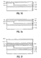
- the interconnect structure of Figure 2 is formed by a damascene or dual damascene process, such as the process shown in Figures 3(a)-3(j) .
- the process preferably begins with deposition of adhesion promoter layer (111) on substrate (110), and is followed by deposition of ILD layer (112) on adhesion promoter layer (111), as shown in Figure 4(a).
- Adhesion promoter layer (111) and ILD layer (112) may be deposited by any suitable method. For example, if adhesion promoter layer (111) is formed of AP4000, the adhesion promoter solution may be applied by a spin-coating process, followed by a baking step. If SiLKTM is used for ILD layer (112), the resin may be applied by a spin-coating process, followed by a baking step to remove solvent and then a thermal curing step.
- Hardmask layer (113) is then deposited on ILD layer (112), as shown in Figure 3(a) .
- Hardmask layer (113) may be deposited by any suitable method, but is preferably deposited by chemical vapor deposition (CVD) directly onto ILD layer (112).
- CVD chemical vapor deposition
- a silicon nitride hardmask layer (113) is deposited in a CVD reactor at a pressure in the range of about 0.1 to 10 torr (13,33-1333 Pa), most preferably in the range of about 1 to 5 torr (133,32-666 Pa), using a combination of gases that may include, but are not limited to, silane (SiH 4 ), ammonia (NH 3 ), nitrogen (N 2 ) and helium (He).
- a typical deposition process uses a flow of SiH 4 in the range of about 100 to 700 sccm, a flow of NH 3 in the range of about 100 to 5000 sccm, and a flow of N 2 in the range of about 100 to 5000 sccm.
- the deposition temperature is typically within the range of about 150 to 500°C, most preferably in the range of about 350 to 450°C.
- the high-frequency radio-frequency (RF) power is typically in the range of about 50 to 700 watts per showerhead, and the low frequency RF power is typically in the range of about 50 to 500 watts per showerhead.
- the final deposition thickness is preferably in the range of about 10 to 100 nm, and most preferably in the range of about 25 to 70 nm.
- This silicon nitride hardmask film preferably has a composition of about 30 to 45 atomic % silicon, about 30 to 55 atomic % nitrogen, and about 10 to 25 atomic % hydrogen. Most preferably, this silicon nitride hardmask film has a composition of about 41 atomic % silicon, about 41 atomic % nitrogen, and about 17.5 atomic % hydrogen.
- a silicon carbide hardmask layer (113) is deposited in a CVD reactor at a pressure of about 0.1 to 20 torr (13,33 - 2666 Pa), most preferably in the range of about 1 to 10 torr (133,3 - 1333 Pa), using a combination of gases that may include, but are not limited to, SiH 4 , NH 3 , N 2 , He, trimethylsilane (3MS), and/or tetramethylsilane (4MS).
- a typical deposition process uses a flow of 3MS in the range of about 50 to 500 sccm and a flow of He in the range of about 50 to 2000 sccm.
- the deposition temperature is typically within the range of about 150 to 500°C, most preferably in the range of about 300 to 400°C.
- the RF power is typically in the range of about 150 to 700 watts per showerhead, most preferably in the range of about 100 to 500 watts per showerhead.
- the final deposition thickness is preferably in the range of about 10 to 100 nm, and most preferably in the range of about 25 to 70 nm.
- This amorphous hydrogenated silicon carbide hardmask film preferably has a composition of about 27 atomic % silicon, about 36 atomic % carbon and about 37 atomic % hydrogen.
- Hardmask layer (113) may function as a patterning layer to assist in later etching of ILD layer (112) to form a trench for conductor (115). Hardmask layer (113) may also serve as a polish stop layer during a subsequent CMP step to remove excess metal.
- additional sacrificial hardmask layers may be deposited.
- additional sacrificial hardmask layers may be deposited.
- a series of hardmask layers may be deposited, such as the hardmask layers described in co-pending U.S. Patent Application Ser. No. 09/550,943, filed April 14, 2000 and titled "Protective Hardmask for Producing Interconnect Structures," the disclosure of which is incorporated herein by reference.
- an additional silicon nitride film may be deposited, followed by a silicon oxide deposition.
- an additional silicon nitride hardmask film is deposited in a CVD reactor at a pressure in the range of about 0.1 to 10 torr (13,33 - 1333 Pa), most preferably in the range of about 1 to 5 torr (133,3 - 666 Pa), using a combination of gases that may include, but are not limited to, SiH 4 , NH 3 , N 2 and/or He.
- a typical deposition process uses a flow of SiH 4 in the range of about 100 to 700 sccm, a flow of NH 3 in the range of about 100 to 5000 sccm, and a flow of N 2 in the range of about 100 to 5000 sccm.
- the deposition temperature is typically within the range of about 150 to 500°C, most preferably in the range of about 350 to 450°C.
- the high frequency RF power is typically in the range of about 50 to 700 watts per showerhead, and the low frequency RF power is typically in the range of about 50 to 500 watts per showerhead.
- the final deposition thickness is preferably in the range of about 10 to 100 nm, most preferably in the range of about 25 to 60 nm.
- This additional silicon nitride hardmask film preferably has a composition of about 41 atomic % silicon, about 41 atomic % nitrogen, and about 17.5 atomic % hydrogen.
- the subsequent silicon oxide hardmask layer is deposited in a CVD reactor at a pressure in the range of about 0.1 to 10 torr (13,33 - 1333 Pa), most preferably in the range of about 1 to 5 torr (133,3 - 666 Pa), using a combination of gases that may include, but are not limited to, SiH 4 , N 2 O, N 2 , and O 2 .
- a typical deposition uses a flow of SiH 4 in the range of about 10 to 700 sccm, a flow of N 2 O in the range of about 100 to 20000 sccm, and a flow of N 2 in the range of about 100 to 3000 sccm.
- the deposition temperature is typically in the range of about 150 to 500°C, most preferably in the range of about 350 to 450°C.
- RF power is typically in the range of about 150 to 500 watts per showerhead, most preferably in the range of about 50 to 3000 watts per showerhead.
- the final deposition thickness is preferably in the range of about 30 to 250 nm, most preferably in the range of about 50 to 200 nm.
- This additional silicon oxide hardmask layer preferably has a composition of about 33 atomic % silicon, about 63 atomic % oxygen, and less than about 1 atomic % hydrogen.
- At least one trench (115a) is formed using a conventional photolithography patterning and etching process.
- a photoresist material (not shown) is deposited on hardmask layer (113).
- the photolithography material is exposed to ultraviolet (UV) radiation through a mask, and then the photoresist material is developed.
- UV radiation ultraviolet
- exposed portions of the photoresist may be rendered either soluble or insoluble during development. These soluble portions of the photoresist are then removed, leaving behind a photoresist pattern matching the desired pattern of trenches.
- Trench (115a) is then formed by removing hardmask layer (113) and a portion of ILD layer (112) by, for example, reactive ion etching (RIE), in areas not protected by the photoresist.
- Hardmask layer (113) may assist in this etching step as follows. Hardmask layer (113) may be etched first in areas not covered by the photoresist, then the photoresist may be removed, leaving behind a patterned hardmask layer (113) matching the photoresist pattern. Then, ILD layer (112) may be etched in areas not covered by hardmask layer (113).
- Diffusion barrier liner (114) may be deposited by any suitable method, such as by physical vapor deposition (PVD), chemical vapor deposition (CVD) or ionized physical vapor deposition (I-PVD).
- Conductive material (115) may deposited in trench (115 a ) by any suitable method, such as by plating technology. Excess liner (114) and conductive material (115) may be removed in a CMP process, in which the top surface of conductor (115) is made coplanar with the top surface of hardmask layer (113). Hardmask layer (113) may serve as a polish-stop layer during this CMP step, thereby protecting ILD layer (112) from damage during polishing. Sacrificial hardmask layers (not shown) may also be removed during this CMP step.
- First cap layer (116) is then deposited on conductor (115) and hardmask layer (113), as shown in Figure 3(d) .
- First cap layer (116) is preferably deposited by a HDP CVD process, but may be deposited by other processes such as by PVD, PE CVD, or spin-on techniques.
- First cap layer (116) may be formed of silicon nitride, silicon carbide, boron nitride or other suitable dielectric material.
- first cap layer (116) is a HDP CVD silicon nitride film deposited in a CVD reactor at a pressure in the range of about 0.1 to 50 milli-torr (0,0133 to 6,67 Pa), most preferably at a pressure in the range of about 5 to 20 milli-torr (0,67 to 2,67 Pa).
- the deposition gases may include, but are not limited to, SiH 4 , N 2 , and Ar or He.
- a typical deposition uses a flow of SiH 4 in the range of about 5 to 125 sccm, a flow of N 2 in the range of about 50 to 1000 sccm, and a flow of Ar in the range of about 20 to 1000 sccm.
- the deposition temperature is typically in the range of about 200 to 500°C, with a range of about 300 to 450°C most preferred.
- Radiofrequency (RF) power is typically in the range of about 1700 to 2500 watts per showerhead, and most preferably in the range of about 1750 to 1950 watts per showerhead.
- the final deposition thickness is preferably in the range of about 2.5 to 70 nm, and most preferably in the range of about 5 to 35 nm.
- This HDP silicon nitride cap layer preferably has a composition of about 30 to 50 atomic % silicon, about 40 to 65 atomic % nitrogen, and about 5 to 13 atomic % hydrogen, most preferably about 40 atomic % silicon, about 52 atomic % nitrogen, and about 8 atomic % hydrogen.
- Second cap layer (117) is deposited, as shown in Figure 3(e) .
- Second cap layer (117) is deposited by a PE CVD process.
- Second cap layer (117) may be formed of silicon nitride, silicon carbide, boron nitride or other suitable dielectric. These PE CVD films may be either hydrogenous or amorphous or both. While it is most preferred that deposition of second cap layer (117) occurs without interruption of the vacuum environment of the first cap layer (116) deposition and without exposing the substrate to atmospheric pressure, it is possible for the second cap layer deposition to occur with a vacuum interruption after the first cap layer (116) deposition.
- second cap layer (117) is a PE CVD silicon nitride layer, and is deposited in a CVD reactor at a pressure in the range of about 0.1 to 10 torr (13,33 - 1333 Pa), most preferably in the range of about 1 to 7 torr (133,3 - 933 Pa), using a combination of gases that may include, but are not limited to, SiH 4 , NH 3 , N 2 and He.
- a typical deposition uses a flow of SiH 4 in the range of about 10 to 500 sccm, a flow of NH 3 in the range of about 100 to 3000 sccm, and a flow of N 2 in the range of about 500 to 25000 sccm.
- the deposition temperature is typically in the range of about 150 to 500°C, most preferably in the range of about 350 and 450°C.
- the high frequency RF power is typically in the range of about 25 to 700 watts per showerhead, most preferably in the range of about 50 to 250 watts per showerhead.
- the low frequency RF power is typically in the range of about 0 to 500 watts per showerhead.
- the final deposition thickness is preferably in the range of about 10 to 100 nm, and most preferably in the range of about 25 to 70 nm.
- This PE CVD silicon nitride cap layer preferably has a composition of about 30 to 45 atomic % silicon, about 40 to 65 atomic % nitrogen, and about 10 to 25 atomic % hydrogen.
- a particularly preferred composition for second cap layer (117) is about 37 atomic % silicon, about 48 atomic % nitrogen, and about 15 atomic % hydrogen.
- second cap layer (117) is a PE CVD amorphous hydrogenated silicon carbide layer, and is deposited in a CVD reactor at a pressure in the range of about 0.1 to 20 torr (13,33 - 2666 Pa), most preferably in the range of about 1 to 10 torr (133,3 - 1333 Pa), using a combination of gases that may include, but is not limited to, SiH 4 , NH 3 , N 2 , He, trimethylsilane (3MS), or tetramethylsilane (4MS).
- a typical deposition uses a flow of 3MS in the range of about 50 to 500 sccm, and a flow of He in the range of about 50 to 2000 sccm.
- the deposition temperature is typically in the range of about 150 to 500°C, most preferably in the range of about 300 to 400°C.
- the RF power is typically in the range of about 150 to 700 watts per showerhead, most preferably in the range of about 100 to 500 watts per showerhead.
- the final deposition thickness is preferably in the range of about 10 to 100 nm, and most preferably in the range of about 25 to 70 nm.
- This amorphous hydrogenated silicon carbide film preferably has a composition of about 20 to 40 atomic % silicon, about 20 to 50 atomic % carbon, and about 20 to 45 atomic % hydrogen, most preferably about 27 atomic % silicon, about 36 atomic % carbon, and about 37 atomic % hydrogen.
- second cap layer (117) is a PE CVD amorphous hydrogenated nitrogenated silicon carbide layer, and is deposited in a CVD reactor at a pressure in the range of about 0.1 to 20 torr (13,33 - 2666 Pa), most preferably in the range of about 1 to 10 torr (133,3 - 1333 Pa), using a combination of gases that may include, but is not limited to, SiH 4 , NH 3 , N 2 , He, 3MS, 4MS and other methyl silanes.
- This second cap layer (117) is preferably deposited using 3MS or 4MS at a flow rate in the range of about 50 to 500 sccm, and N 2 at a flow rate in the range of about 50 to 500 sccm.
- the deposition temperature is preferably in the range of about 150 to 500°C, most preferably in the range of about 300 to 400°C.
- the RF power is preferably in the range of about 100 to 700 watts per showerhead, most preferably in the range of about 200 to 500 watts.
- the final deposition thickness is preferably in the range of about 10 to 100 nm, and most preferably in the range of about 25 to 70 nm
- This amorphous hydrogenated nitrogenated silicon carbide film preferably has a composition of about 20 to 34 atomic % silicon, about 12 to 34 atomic % carbon, about 5 to 30 atomic % nitrogen and about 20 to 50 atomic % hydrogen, most preferably about 22 to 30 atomic % silicon, about 15 to 30 atomic % carbon, about 10 to 22 atomic % nitrogen and about 30 to 45 atomic % hydrogen.
- Second cap layer (117) may be formed of a series of thin PE CVD films, where the total thickness is in the range of about 10 to 100 nm. These thin PE CVD films may be formed of the same material, such as silicon nitride, or they may be formed of different or alternating materials, such as silicon nitride, silicon carbide, silicon oxide, silicon oxycarbide and/or silicon oxycarbonitride. As discussed previously, second cap layer (117) may comprise alternating films of different material or a series of films of the same material together with films of a different material.
- a plasma pre-cleaning step may be performed in the CVD reactor.
- a typical plasma pre-cleaning step uses a source of hydrogen such as NH 3 or H 2 at a flow rate in the range of about 50 to 700 sccm, and is performed at a substrate temperature in the range of about 15 to 500°C, most preferably at a substrate temperature in the range of about 20 to 400°C, for a time of about 5 to 500 seconds and most preferably about 10 to 100 seconds:
- the RF power is in the range of about 100 to 10,000 watts, and most preferably in the range of about 1000 to 5000 watts during this cleaning step.
- other gases such as He, argon (Ar) or N 2 may be added at a flow rate in the range of about 50 to 20,000 sccm.
- Figures 3(a)-3(e) illustrate the formation of the first interconnect level, which consists of adhesion promoter layer (111), ILD layer (112), hardmask layer (113), diffusion barrier liner (114), conductor (115), first cap layer (116), and second cap layer (117).
- the formation of the second interconnect level begins with deposition of adhesion promoter layer (118), ILD layer (119) and hardmask layer (120).
- Adhesion promoter layer (118) may be deposited using the same method as that for adhesion promoter layer (111).
- ILD layer (119) may be deposited using the same method as that for ILD layer (112), and hardmask layer (120) may be deposited using the same method as that for hardmask layer (113). Additional sacrificial hardmask layers (not shown) may be deposited on primary hardmask layer (120).
- Figures 3(g) and 3(h) illustrate the formation of via (122 a ) and trench (122 b ).
- at least one via (122 a ) may be formed in hardmask layer (120), ILD layer (119), adhesion promoter layer (118) and cap layers (117) and (116), using a conventional photolithography patterning and etching process, as shown in Figure 3(g) .
- at least one trench (122 b ) may be formed in hardmask layer (120) and a portion of ILD layer (119), using a conventional photolithography process, as shown in Figure 3(h) .
- Via (122 a ) and trench (122 b ) may be formed using the same photolithography process as that used to form trench (115 a ).
- via (122 a ) and trench (122 b ) may be formed by first patterning and etching a trench in hardmask layer (120) and ILD layer (119), where the trench has a depth equal to the depth of trench (122 b ), but has a length equal to the length of trench (122 b ) and the width of via (122 a ) combined. Then via (122 a ) may then be formed by etching through the remainder of ILD layer (119), adhesion promoter layer (118) and cap layers (117) and (116).
- Diffusion barrier liner (121) may be deposited by the same method used for diffusion barrier liner (114), and conductive material (122) may deposited by the same method used for conductor (115). Excess liner (121) and conductive material (122) may be removed in a CMP process, in which the top surface of conductor (122) is made coplanar with the top surface of hardmask layer (120). Sacrificial hardmask layers (not shown) may also be removed during this CMP step. Hardmask layer (120) may serve as a polish-stop layer during this CMP step, thereby protecting ILD layer (119) from damage during polishing.
- Cap layers (123) and (124) are then deposited on conductor (122) and hardmask layer (120), as shown in Figure 3(j) .
- First cap layer (123) may be deposited using the same process as that for first cap layer (116), and second cap layer (124) may be deposited using the same process as that for second cap layer (117).
- the present invention is useful in the manufacture of high speed semiconductor microprocessors, application specific integrated circuits (ASICs), and other high speed integrated circuit devices. More particularly, the bilayer cap of this invention is useful in advanced back-end-of-line (BEOL) interconnect structures for semiconductor devices using low-k dielectric materials.
- BEOL back-end-of-line
Landscapes
- Internal Circuitry In Semiconductor Integrated Circuit Devices (AREA)
- Chemical Vapour Deposition (AREA)
- Formation Of Insulating Films (AREA)
- Valve-Gear Or Valve Arrangements (AREA)
Abstract
Description
- This invention relates generally to the manufacture of high speed semiconductor microprocessors, application specific integrated circuits (ASICs), and other high speed integrated circuit devices. More particularly, this invention relates to a novel bilayer cap in advanced back-end-of-line (BEOL) interconnect structures for semiconductor devices using low-k dielectric materials. The invention is specifically directed to a bilayer cap comprising high-density plasma chemical vapor deposition (HDP CVD) materials and plasma-enhanced chemical vapor deposition (PE CVD) material in advanced BEOL metallization structures, and a method of forming the bilayer cap.
-
JP 2000 332102A - In semiconductor devices, aluminum and aluminum alloys have been used as the traditional interconnect metallurgies. While aluminum-based metallurgies have been the material of choice for use as metal interconnects over the past years, concern now exists as to whether aluminum will meet the demands required as circuit density and speeds for semiconductor devices increase. Because of these growing concerns, other materials have been investigated as possible replacements for aluminum-based metallurgies.
- One highly advantageous material now being considered as a potential replacement for aluminum metallurgies is copper, because of its lower susceptibility to electromigration failure as compared to aluminum, as well as its lower resistivity.
- Despite these advantages, copper suffers from an important disadvantage. Copper readily diffuses into the surrounding dielectric material during subsequent processing steps. To inhibit the diffusion of copper, copper interconnects are often capped with a protective barrier layer. One method of capping involves the use of a conductive barrier layer of tantalum, titanium or tungsten, in pure or alloy form, along the sidewalls and bottom of the copper interconnection. To cap the upper surface of the copper interconnection, a dielectric material such as silicon nitride (Si3N4) is typically employed.
-
Figure 1 illustrates a conventional BEOL interconnect structure utilizing copper metallization and the protective cap layers described above. The interconnect structure comprises a lower substrate (10) which may contain logic circuit elements such as transistors. A dielectric layer (12), commonly known as an inter-layer dielectric (ILD), overlies the substrate (10). ILD layer (12) may be formed of silicon dioxide (SiO2). However, in advanced interconnect structures, ILD layer (12) is preferably a low-k polymeric thermoset material such as SiLK™ (an aromatic hydrocarbon thermosetting polymer available from The Dow Chemical Company). An adhesion promoter layer (11) may be disposed between the substrate (10) and ILD layer (12). A layer of silicon nitride (13) is optionally disposed on ILD layer (12). Silicon nitride layer (13) is commonly known as a hardmask layer or polish stop layer. At least one conductor (15) is embedded in ILD layer (12). Conductor (15) is preferably copper in advanced interconnect structures, but alternatively may be aluminum or other conductive material. When conductor (15) is copper, a diffusion barrier liner (14) is preferably disposed between ILD layer (12) and conductor (15). Diffusion barrier liner (14) is typically comprised of tantalum, titanium, tungsten or nitrides of these metals. The top surface of conductor (15) is made coplanar with the top surface of silicon nitride layer (13), usually by a chemical-mechanical polish (CMP) step. A cap layer (16), also typically of silicon nitride, is disposed on conductor (15) and silicon nitride layer (13). Cap layer (16) acts as a diffusion barrier to prevent diffusion of copper from conductor (15) into the surrounding dielectric material during subsequent processing steps. - A first interconnect level is defined by adhesion promoter layer (11), ILD layer (12), silicon nitride layer (13), diffusion barrier liner (14), conductor (15), and cap layer (16) in the interconnect structure shown in
Figure 1 . A second interconnect level, shown above the first interconnect level inFigure 1 , includes adhesion promoter layer (18), ILD layer (19), silicon nitride layer (20), diffusion barrier liner (21), conductor (22), and cap layer (23). The first and second levels may be formed by conventional damascene processes. For example, formation of the second interconnect level begins with deposition of adhesion promoter layer (18). Next, the ILD material (19) is deposited onto adhesion promoter layer (18). If the ILD material is a low-k polymeric thermoset material such as SiLK™, the ILD material is typically spin-applied, given a post apply hot bake to remove solvent, and cured at elevated temperature. Next, silicon nitride layer (20) is deposited on the ILD. Silicon nitride layer (20), ILD layer (19), adhesion promoter layer (18) and cap layer (16) are then patterned, using a conventional photolithography and etching process, to form at least one trench and via. The trenches and vias are typically lined with diffusion barrier liner (21). The trenches and vias are then filled with a metal such as copper to form conductor (22) in a conventional dual damascene process. Excess metal is removed by a CMP process. Finally, cap layer (23) is deposited on copper conductor (22) and silicon nitride layer (20). - Due to the need for low temperature processing after copper deposition, cap layers are typically deposited at temperatures below 450°C. Accordingly, cap layer deposition is typically performed using plasma-enhanced chemical vapor deposition (PE CVD) or high density plasma chemical vapor deposition (HDP CVD) wherein the deposition temperature generally ranges from about 200°C to about 500°C.
- PE CVD and HDP CVD films have been used for many other applications in semiconductor device manufacturing. However, in using a cap layer such as silicon nitride for copper interconnects, conventional PE CVD or HDP CVD silicon nitride films create reliability problems.
- HDP CVD films such as silicon nitride provide superior electromigration protection, as compared to PE CVD films, because HDP CVD films more readily stop the movement of copper atoms along the interconnect surface in the cap layer. However, in a conventional HDP deposition process, a seam is formed in the HDP CVD cap layer, and a crack in the cap layer often develops at this seam due to stress within the structure. If the crack develops in a portion of the cap layer overlying a copper conductor, the copper conductor may be readily exposed to moisture and other sources of oxygen. If the crack develops in a portion of the cap layer overlying the ILD, the copper conductor may be exposed to moisture diffusing through the ILD. In the latter case, the seam is of relatively minor concern in interconnect structures utilizing silicon dioxide as the ILD material, because the rate of moisture diffusion through silicon dioxide is very low. However, in interconnect structures utilizing low-k polymeric thermoset dielectric materials such as SiLK™, this seam is of greater concern, because the rate of moisture diffusion through most spin-on and CVD low-k materials is relatively high.
- Moreover, any crack in the cap layer may lead to copper diffusion into the ILD through the seam. As a result of this copper diffusion, a copper nodule may form under the cap layer through the seams. This copper nodule may lead to leakage between adjacent interconnect lines.
- Another significant disadvantage occurs when HDP CVD films are integrated with low-k dielectric materials. The energetic reactions of the HDP CVD process can enable interaction with and within the low-k materials causing undesirable changes to occur.
- Such changes in low-k dielectric materials can be significantly mitigated by the use of PE CVD films. Moreover, in typical PE CVD films, no seam is formed during the deposition process. For this reason, PE CVD cap layers have been used to cap copper interconnect structures in earlier ground-rule devices, such as the 0.22 µm technology node. However, in more advanced ground-rule devices, such as the 0.18 µm technology node, PE CVD films have been found to be inferior to cap layers formed by other deposition techniques such as HDP CVD.
- In particular, PE CVD films generally exhibit poorer adhesion to the copper surface. Typical PE CVD silicon nitride films exhibit adhesion values in the range of about 5 to less than 10 joules/m2, whereas typical HDP CVD silicon nitride films exhibit adhesion values of about 20 joules/m2, as determined by a four-point bend adhesion testing technique. PE CVD films may delaminate and form blisters over patterned copper lines, particularly during subsequent dielectric depositions, metallization, and chemical-mechanical polishing. After being deposited onto copper metallurgy, additional insulating layers generally will be deposited over the cap layer. However, subsequent deposition of insulating layers onto the cap layer will produce stress which can cause the cap layer to peel from the copper surface. This delamination results in several catastrophic failure mechanisms, including lifting interlayer dielectrics, lifting copper conductors, copper diffusion from uncapped copper lines, and electromigration. Such results are generally seen in dual damascene processing where delamination of the silicon nitride hardmask layer generally occurs during copper chemical-mechanical polishing.
- Thus, there is a need in the art for an interconnect structure cap layer exhibiting the superior electromigration protection and adhesion characteristics of HDP CVD films, and the superior coverage of PE CVD films.
- The problems described above are addressed through use of the present invention, which is directed to a method of forming an interconnect structure on a substrate. The method comprises the steps of: depositing a dielectric material on the substrate, thereby forming a dielectric layer, depositing a hardmask material on said dielectric layer, thereby forming a hardmask layer, said hardmask layer having a top surface; forming at least one opening in said dielectric layer; filling said opening with a conductive material, thereby forming at least one conductor, said conductor having a top surface coplanar with the top surface of said hardmask layer; depositing a first material on said conductor by a high density plasma chemical vapor deposition (HDP CVD) process, thereby forming a first cap layer; and depositing a second material on said first cap layer, by a plasma-enhanced chemical vapor deposition (PE CVD) process, thereby forming a second cap layer.
- The features of the invention believed to be novel and the elements characteristic of the invention are set forth with particularity in the appended claims. The drawings are for illustration purposes only and are not drawn to scale. Furthermore, like numbers represent like features in the drawings. The invention itself, however, both as to organization and method of operation, may best be understood by reference to the detailed description which follows, taken in conjunction with the accompanying drawings, in which:
-
Figure 1 is a schematic cross-sectional view of a partially-fabricated integrated circuit device illustrating a prior art interconnect structure; -
Figure 2 is a schematic cross-sectional view of a partially-fabricated integrated circuit device illustrating an interconnect structure in accordance with a preferred embodiment of the invention; and -
Figures 3(a)-3(j) illustrate a method for forming the interconnect structure ofFigure 2 . - The invention will now be described by reference to the accompanying figures. In the figures, various aspects of the structures have been shown and schematically represented in a simplified manner to more clearly describe and illustrate the invention. For example, the figures are not intended to be to scale. In addition, the vertical cross-sections of the various aspects of the structures are illustrated as being rectangular in shape. Those skilled in the art will appreciate, however, that with practical structures these aspects will most likely incorporate more tapered features. Moreover, the invention is not limited to constructions of any particular shape.
- Although certain aspects of the invention will be described with respect to a structure comprising copper, the invention is not so limited. Although copper is the preferred conductive material, the structure of the present invention may comprise any suitable conductive material, such as aluminum.
- Referring to
Figure 2 , a preferred embodiment of the interconnect structure produced by the method of the invention comprises a lower substrate (110) which may contain logic circuit elements such as transistors. A dielectric layer (112), commonly known as an inter-layer dielectric (ILD), overlies the substrate (110). An adhesion promoter layer (111) may be disposed between the substrate (110) and ILD layer (112). A hardmask layer (113) is preferably disposed on ILD layer (112). At least one conductor (115) is embedded in ILD layer (112) and hardmask layer (113). A diffusion barrier liner (114) may be disposed between ILD layer (112) and conductor (115). The top surface of conductor (115) is made coplanar with the top surface of hardmask layer (113), usually by a chemical-mechanical polish (CMP) step. A first cap layer (116) is disposed on conductor (115) and hardmask layer (113), and a second cap layer (117) is disposed on first cap layer (116). - A first interconnect level is defined by adhesion promoter layer (111), ILD layer (112), hardmask layer (113), diffusion barrier liner (114), conductor (115), first cap layer (116), and second cap layer (117) in the interconnect structure shown in
Figure 2 . A second interconnect level, shown above the first interconnect level inFigure 2 , includes adhesion promoter layer (118), ILD layers (119), hardmask layer (120), diffusion barrier liner (121), conductor (122), first cap layer (123), and second cap layer (124). - ILD layers (112) and (119) may be formed of any suitable dielectric material, although low-k dielectric materials are preferred. Suitable dielectric materials include carbon-doped silicon dioxide materials; fluorinated silicate glass (FSG); organic polymeric thermoset materials, silicon oxycarbide; SiCOH dielectrics; fluorine doped silicon oxide; spin-on glasses; silsesquioxanes, including hydrogen silsesquioxane (HSQ), methyl silsesquioxane (MSQ) and mixtures or copolymers of HSQ and MSQ; benzocyclobutene (BCB) -based polymer dielectrics, and any silicon-containing low-k dielectric. Examples of spin-on low-k films with SiCOH-type composition using silsesquioxane chemistry include HOSP™ (available from Honeywell), JSR 5109 and 5108 (available from Japan Synthetic Rubber), Zirkon™ (available from Shipley Microelectronics, a division of Rohm and Haas), and porous low-k (ELk) materials (available from Applied Materials). Examples of carbon-doped silicon dioxide materials, or organosilanes, include Black Diamond™ (available from Applied Materials) and Coral™ (available from Novellus). An example of an HSQ material is FOx™ (available from Dow Coming). For this embodiment, preferred dielectric materials are organic polymeric thermoset materials, consisting essentially of carbon, oxygen and hydrogen. Preferred dielectric materials include the low-k polyarylene ether polymeric material known as SiLK™ (available from The Dow Chemical Company), and the low-k polymeric material known as FLARE™ (available from Honeywell). ILD layers (112) and (119) may each be about 100 nm to about 1000 nm thick, but these layers are each preferably about 600 nm thick. The dielectric constant for ILD layers (112) and (119) is preferably about 1.8 to about 3.5, and most preferably about 2.5 to about 2.9.
- Alternatively, ILD layers (112) and (119) may be formed of a porous dielectric material, such as MesoELK™ (available from Air Products) and XLK™ (a porous version of FOx, available from Dow Corning). For example, If ILD layers (112) and (119) are formed of such porous dielectric material, the dielectric constant of these layers is preferably less than about 2.6, and is most preferably about 1.5 to 2.5. It is particularly preferred to use an organic polymeric thermoset material having a dielectric constant of about 1.8 to 2.2.
- Adhesion promoter layers (111) and (118) are preferably about 9 nm thick, and may be composed of any material suitable for enhancing adhesion of the dielectric material in ILD layers (112) and (119) to the underlying surfaces. For example, if SiLK™ is used for ILD layers (112) and (119), adhesion promoter layers (111) and (118) may be formed of an adhesion promoter known as AP4000 (also available from The Dow Chemical Company).
- Hardmask layers (113) and (120) may be formed of any suitable dielectric material. In one preferred embodiment, hardmask layers (113) and (120) are formed of silicon nitride, and preferably have a composition of about 30 to 45 atomic % silicon, about 30 to 55 atomic % nitrogen, and about 10 to 25 atomic % hydrogen. Most preferably, these silicon nitride hardmask layers have a composition of about 41 atomic % silicon, about 41 atomic % nitrogen, and about 17.5 atomic % hydrogen. Alternatively, in another preferred embodiment, hardmask layers (113) and (120) are formed of silicon carbide, and preferably have a composition of about 20 to 40 atomic % silicon, about 20 to 50 atomic % carbon and about 20 to 45 atomic % hydrogen. A particularly preferred composition is about 27 atomic % silicon, about 36 atomic % carbon and about 37 atomic % hydrogen.
- Conductors (115) and (122) may be formed of any suitable conductive material, such as copper or aluminum. Copper is particularly preferred as the conductive material, due to its relatively low resistance. Copper conductors (115) and (122) may contain small concentrations of other elements. Diffusion barrier liners (114) and (121) may comprise one or more of the following materials: tantalum, titanium, tungsten and the nitrides of these metals.
- First cap layers (116) and (123) may be formed of silicon nitride, silicon carbide, boron nitride or other suitable dielectric material, and are formed using a HDP CVD process. It has been discovered that materials deposited using a HDP CVD process provide superior adhesion and superior electromigration resistance. First cap layers (116) and (123) are most preferably formed of HDP CVD silicon nitride having a composition of about 30 to 50 atomic % silicon, about 40 to 65 atomic % nitrogen and about 5 to 13 atomic % hydrogen. A particularly preferred composition for first cap layers (116) and (123) is about 40 atomic % silicon, about 52 atomic % nitrogen, and about 8 atomic % hydrogen. First cap layers (116) and (123) preferably each have a thickness in the range of about 2,5 to 70 nm, and most preferably in the range of about 5 to 35 nm.
- Second cap layers (117) and (124) may be formed of silicon nitride, silicon carbide, boron nitride, silicon oxide or other suitable dielectric material, but are formed using a PE CVD process. Second cap layers (117) and (124) are most preferably formed of PE CVD silicon nitride having a composition of about 30 to 45 atomic % silicon, about 40 to 65 atomic % nitrogen, and about 10 to 25 atomic % hydrogen. A particularly preferred composition for second cap layers (117) and (124) is about 37 atomic % silicon, about 48 atomic % nitrogen, and about 15 atomic % hydrogen. In another preferred embodiment, second cap layers (117) and (124) are formed of PE CVD amorphous hydrogenated silicon carbide having a composition of about 20 to 40 atomic % silicon, about 20 to 50 atomic % nitrogen, and about 20 to 45 atomic % hydrogen, most preferably about 27 atomic % silicon, about 36 atomic % carbon, and about 37 atomic % hydrogen. In yet another preferred embodiment, second cap layers (117) and (124) are formed of PE CVD amorphous hydrogenated nitrogenated silicon carbide having a composition of about 20 to 34 atomic % silicon, about 12 to 34 atomic % carbon, about 5 to 30 atomic % nitrogen and about 20 to 50 atomic % hydrogen, most preferably about 22 to 30 atomic % silicon, about 15 to 30 atomic % carbon, about 10 to 22 atomic % nitrogen and about 30 to 45 atomic % hydrogen. Second cap layers (117) and (124) preferably each have a thickness in the range of about 10 to 100 nm, and most preferably in the range of about 25 to 70 nm.
- Second cap layers (117) and (124) may be formed of a series of thin PE CVD films, where the total thickness is in the range of about 10 to 100 nm. In one embodiment, these thin PE CVD films each may be formed of the same material, such as silicon nitride. In another embodiment, the thin PE CVD films may be formed of different materials, such as silicon nitride, silicon carbide, silicon oxide, silicon oxycarbide, and/or silicon oxycarbonitride. The second cap layer also may be formed of alternating layers of high-permeability or high-affinity dielectric films and low-permeability or low-affinity dielectric films, such as the laminated diffusion barrier described in co-pending
U.S. Application Ser. No. 09/858,687, filed May 16, 2001 - The interconnect structure of
Figure 2 is formed by a damascene or dual damascene process, such as the process shown inFigures 3(a)-3(j) . The process preferably begins with deposition of adhesion promoter layer (111) on substrate (110), and is followed by deposition of ILD layer (112) on adhesion promoter layer (111), as shown in Figure 4(a). Adhesion promoter layer (111) and ILD layer (112) may be deposited by any suitable method. For example, if adhesion promoter layer (111) is formed of AP4000, the adhesion promoter solution may be applied by a spin-coating process, followed by a baking step. If SiLK™ is used for ILD layer (112), the resin may be applied by a spin-coating process, followed by a baking step to remove solvent and then a thermal curing step. - Hardmask layer (113) is then deposited on ILD layer (112), as shown in
Figure 3(a) . Hardmask layer (113) may be deposited by any suitable method, but is preferably deposited by chemical vapor deposition (CVD) directly onto ILD layer (112). In one preferred embodiment, a silicon nitride hardmask layer (113) is deposited in a CVD reactor at a pressure in the range of about 0.1 to 10 torr (13,33-1333 Pa), most preferably in the range of about 1 to 5 torr (133,32-666 Pa), using a combination of gases that may include, but are not limited to, silane (SiH4), ammonia (NH3), nitrogen (N2) and helium (He). A typical deposition process uses a flow of SiH4 in the range of about 100 to 700 sccm, a flow of NH3 in the range of about 100 to 5000 sccm, and a flow of N2 in the range of about 100 to 5000 sccm. The deposition temperature is typically within the range of about 150 to 500°C, most preferably in the range of about 350 to 450°C. The high-frequency radio-frequency (RF) power is typically in the range of about 50 to 700 watts per showerhead, and the low frequency RF power is typically in the range of about 50 to 500 watts per showerhead. The final deposition thickness is preferably in the range of about 10 to 100 nm, and most preferably in the range of about 25 to 70 nm. This silicon nitride hardmask film preferably has a composition of about 30 to 45 atomic % silicon, about 30 to 55 atomic % nitrogen, and about 10 to 25 atomic % hydrogen. Most preferably, this silicon nitride hardmask film has a composition of about 41 atomic % silicon, about 41 atomic % nitrogen, and about 17.5 atomic % hydrogen. - In another preferred embodiment, a silicon carbide hardmask layer (113) is deposited in a CVD reactor at a pressure of about 0.1 to 20 torr (13,33 - 2666 Pa), most preferably in the range of about 1 to 10 torr (133,3 - 1333 Pa), using a combination of gases that may include, but are not limited to, SiH4, NH3, N2, He, trimethylsilane (3MS), and/or tetramethylsilane (4MS). A typical deposition process uses a flow of 3MS in the range of about 50 to 500 sccm and a flow of He in the range of about 50 to 2000 sccm. The deposition temperature is typically within the range of about 150 to 500°C, most preferably in the range of about 300 to 400°C. The RF power is typically in the range of about 150 to 700 watts per showerhead, most preferably in the range of about 100 to 500 watts per showerhead. The final deposition thickness is preferably in the range of about 10 to 100 nm, and most preferably in the range of about 25 to 70 nm. This amorphous hydrogenated silicon carbide hardmask film preferably has a composition of about 27 atomic % silicon, about 36 atomic % carbon and about 37 atomic % hydrogen.
- Hardmask layer (113) may function as a patterning layer to assist in later etching of ILD layer (112) to form a trench for conductor (115). Hardmask layer (113) may also serve as a polish stop layer during a subsequent CMP step to remove excess metal.
- Following deposition of a silicon nitride or silicon carbide hardmask film, as described above, additional sacrificial hardmask layers (not shown) may be deposited. For example, a series of hardmask layers may be deposited, such as the hardmask layers described in co-pending
U.S. Patent Application Ser. No. 09/550,943, filed April 14, 2000 - The subsequent silicon oxide hardmask layer is deposited in a CVD reactor at a pressure in the range of about 0.1 to 10 torr (13,33 - 1333 Pa), most preferably in the range of about 1 to 5 torr (133,3 - 666 Pa), using a combination of gases that may include, but are not limited to, SiH4, N2O, N2, and O2. A typical deposition uses a flow of SiH4 in the range of about 10 to 700 sccm, a flow of N2O in the range of about 100 to 20000 sccm, and a flow of N2 in the range of about 100 to 3000 sccm. The deposition temperature is typically in the range of about 150 to 500°C, most preferably in the range of about 350 to 450°C. RF power is typically in the range of about 150 to 500 watts per showerhead, most preferably in the range of about 50 to 3000 watts per showerhead. The final deposition thickness is preferably in the range of about 30 to 250 nm, most preferably in the range of about 50 to 200 nm. This additional silicon oxide hardmask layer preferably has a composition of about 33 atomic % silicon, about 63 atomic % oxygen, and less than about 1 atomic % hydrogen.
- In
Figure 3(b) , at least one trench (115a) is formed using a conventional photolithography patterning and etching process. In a typical photolithography process, a photoresist material (not shown) is deposited on hardmask layer (113). The photolithography material is exposed to ultraviolet (UV) radiation through a mask, and then the photoresist material is developed. Depending on the type of photoresist material used, exposed portions of the photoresist may be rendered either soluble or insoluble during development. These soluble portions of the photoresist are then removed, leaving behind a photoresist pattern matching the desired pattern of trenches. Trench (115a) is then formed by removing hardmask layer (113) and a portion of ILD layer (112) by, for example, reactive ion etching (RIE), in areas not protected by the photoresist. Hardmask layer (113) may assist in this etching step as follows. Hardmask layer (113) may be etched first in areas not covered by the photoresist, then the photoresist may be removed, leaving behind a patterned hardmask layer (113) matching the photoresist pattern. Then, ILD layer (112) may be etched in areas not covered by hardmask layer (113). - Following formation of trench (115a), the trench is preferably lined with diffusion barrier liner (114), and then a conductive material is deposited in trench (115a) to form conductor (115). Diffusion barrier liner (114) may be deposited by any suitable method, such as by physical vapor deposition (PVD), chemical vapor deposition (CVD) or ionized physical vapor deposition (I-PVD). Conductive material (115) may deposited in trench (115a) by any suitable method, such as by plating technology. Excess liner (114) and conductive material (115) may be removed in a CMP process, in which the top surface of conductor (115) is made coplanar with the top surface of hardmask layer (113). Hardmask layer (113) may serve as a polish-stop layer during this CMP step, thereby protecting ILD layer (112) from damage during polishing. Sacrificial hardmask layers (not shown) may also be removed during this CMP step.
- First cap layer (116) is then deposited on conductor (115) and hardmask layer (113), as shown in
Figure 3(d) . First cap layer (116) is preferably deposited by a HDP CVD process, but may be deposited by other processes such as by PVD, PE CVD, or spin-on techniques. First cap layer (116) may be formed of silicon nitride, silicon carbide, boron nitride or other suitable dielectric material. - Most preferably, first cap layer (116) is a HDP CVD silicon nitride film deposited in a CVD reactor at a pressure in the range of about 0.1 to 50 milli-torr (0,0133 to 6,67 Pa), most preferably at a pressure in the range of about 5 to 20 milli-torr (0,67 to 2,67 Pa). The deposition gases may include, but are not limited to, SiH4, N2, and Ar or He. A typical deposition uses a flow of SiH4 in the range of about 5 to 125 sccm, a flow of N2 in the range of about 50 to 1000 sccm, and a flow of Ar in the range of about 20 to 1000 sccm. The deposition temperature is typically in the range of about 200 to 500°C, with a range of about 300 to 450°C most preferred. Radiofrequency (RF) power is typically in the range of about 1700 to 2500 watts per showerhead, and most preferably in the range of about 1750 to 1950 watts per showerhead. The final deposition thickness is preferably in the range of about 2.5 to 70 nm, and most preferably in the range of about 5 to 35 nm. This HDP silicon nitride cap layer preferably has a composition of about 30 to 50 atomic % silicon, about 40 to 65 atomic % nitrogen, and about 5 to 13 atomic % hydrogen, most preferably about 40 atomic % silicon, about 52 atomic % nitrogen, and about 8 atomic % hydrogen.
- Following deposition of first cap layer (116), a second cap layer (117) is deposited, as shown in
Figure 3(e) . Second cap layer (117) is deposited by a PE CVD process. Second cap layer (117) may be formed of silicon nitride, silicon carbide, boron nitride or other suitable dielectric. These PE CVD films may be either hydrogenous or amorphous or both. While it is most preferred that deposition of second cap layer (117) occurs without interruption of the vacuum environment of the first cap layer (116) deposition and without exposing the substrate to atmospheric pressure, it is possible for the second cap layer deposition to occur with a vacuum interruption after the first cap layer (116) deposition. - In a most preferred embodiment, second cap layer (117) is a PE CVD silicon nitride layer, and is deposited in a CVD reactor at a pressure in the range of about 0.1 to 10 torr (13,33 - 1333 Pa), most preferably in the range of about 1 to 7 torr (133,3 - 933 Pa), using a combination of gases that may include, but are not limited to, SiH4, NH3, N2 and He. A typical deposition uses a flow of SiH4 in the range of about 10 to 500 sccm, a flow of NH3 in the range of about 100 to 3000 sccm, and a flow of N2 in the range of about 500 to 25000 sccm. The deposition temperature is typically in the range of about 150 to 500°C, most preferably in the range of about 350 and 450°C. The high frequency RF power is typically in the range of about 25 to 700 watts per showerhead, most preferably in the range of about 50 to 250 watts per showerhead. The low frequency RF power is typically in the range of about 0 to 500 watts per showerhead. The final deposition thickness is preferably in the range of about 10 to 100 nm, and most preferably in the range of about 25 to 70 nm. This PE CVD silicon nitride cap layer preferably has a composition of about 30 to 45 atomic % silicon, about 40 to 65 atomic % nitrogen, and about 10 to 25 atomic % hydrogen. A particularly preferred composition for second cap layer (117) is about 37 atomic % silicon, about 48 atomic % nitrogen, and about 15 atomic % hydrogen.
- In another preferred embodiment, second cap layer (117) is a PE CVD amorphous hydrogenated silicon carbide layer, and is deposited in a CVD reactor at a pressure in the range of about 0.1 to 20 torr (13,33 - 2666 Pa), most preferably in the range of about 1 to 10 torr (133,3 - 1333 Pa), using a combination of gases that may include, but is not limited to, SiH4, NH3, N2, He, trimethylsilane (3MS), or tetramethylsilane (4MS). A typical deposition uses a flow of 3MS in the range of about 50 to 500 sccm, and a flow of He in the range of about 50 to 2000 sccm. The deposition temperature is typically in the range of about 150 to 500°C, most preferably in the range of about 300 to 400°C. The RF power is typically in the range of about 150 to 700 watts per showerhead, most preferably in the range of about 100 to 500 watts per showerhead. The final deposition thickness is preferably in the range of about 10 to 100 nm, and most preferably in the range of about 25 to 70 nm. This amorphous hydrogenated silicon carbide film preferably has a composition of about 20 to 40 atomic % silicon, about 20 to 50 atomic % carbon, and about 20 to 45 atomic % hydrogen, most preferably about 27 atomic % silicon, about 36 atomic % carbon, and about 37 atomic % hydrogen.
- In yet another preferred embodiment, second cap layer (117) is a PE CVD amorphous hydrogenated nitrogenated silicon carbide layer, and is deposited in a CVD reactor at a pressure in the range of about 0.1 to 20 torr (13,33 - 2666 Pa), most preferably in the range of about 1 to 10 torr (133,3 - 1333 Pa), using a combination of gases that may include, but is not limited to, SiH4, NH3, N2, He, 3MS, 4MS and other methyl silanes. This second cap layer (117) is preferably deposited using 3MS or 4MS at a flow rate in the range of about 50 to 500 sccm, and N2 at a flow rate in the range of about 50 to 500 sccm. The deposition temperature is preferably in the range of about 150 to 500°C, most preferably in the range of about 300 to 400°C. The RF power is preferably in the range of about 100 to 700 watts per showerhead, most preferably in the range of about 200 to 500 watts. The final deposition thickness is preferably in the range of about 10 to 100 nm, and most preferably in the range of about 25 to 70 nm This amorphous hydrogenated nitrogenated silicon carbide film preferably has a composition of about 20 to 34 atomic % silicon, about 12 to 34 atomic % carbon, about 5 to 30 atomic % nitrogen and about 20 to 50 atomic % hydrogen, most preferably about 22 to 30 atomic % silicon, about 15 to 30 atomic % carbon, about 10 to 22 atomic % nitrogen and about 30 to 45 atomic % hydrogen.
- Second cap layer (117) may be formed of a series of thin PE CVD films, where the total thickness is in the range of about 10 to 100 nm. These thin PE CVD films may be formed of the same material, such as silicon nitride, or they may be formed of different or alternating materials, such as silicon nitride, silicon carbide, silicon oxide, silicon oxycarbide and/or silicon oxycarbonitride. As discussed previously, second cap layer (117) may comprise alternating films of different material or a series of films of the same material together with films of a different material.
- Prior to deposition of first cap layer (116), a plasma pre-cleaning step may be performed in the CVD reactor. A typical plasma pre-cleaning step uses a source of hydrogen such as NH3 or H2 at a flow rate in the range of about 50 to 700 sccm, and is performed at a substrate temperature in the range of about 15 to 500°C, most preferably at a substrate temperature in the range of about 20 to 400°C, for a time of about 5 to 500 seconds and most preferably about 10 to 100 seconds: The RF power is in the range of about 100 to 10,000 watts, and most preferably in the range of about 1000 to 5000 watts during this cleaning step. Optionally, other gases such as He, argon (Ar) or N2 may be added at a flow rate in the range of about 50 to 20,000 sccm.
-
Figures 3(a)-3(e) illustrate the formation of the first interconnect level, which consists of adhesion promoter layer (111), ILD layer (112), hardmask layer (113), diffusion barrier liner (114), conductor (115), first cap layer (116), and second cap layer (117). InFigure 3(f) , the formation of the second interconnect level begins with deposition of adhesion promoter layer (118), ILD layer (119) and hardmask layer (120). Adhesion promoter layer (118) may be deposited using the same method as that for adhesion promoter layer (111). Likewise, ILD layer (119) may be deposited using the same method as that for ILD layer (112), and hardmask layer (120) may be deposited using the same method as that for hardmask layer (113). Additional sacrificial hardmask layers (not shown) may be deposited on primary hardmask layer (120). -
Figures 3(g) and 3(h) illustrate the formation of via (122a) and trench (122b). First, at least one via (122a) may be formed in hardmask layer (120), ILD layer (119), adhesion promoter layer (118) and cap layers (117) and (116), using a conventional photolithography patterning and etching process, as shown inFigure 3(g) . Then, at least one trench (122b) may be formed in hardmask layer (120) and a portion of ILD layer (119), using a conventional photolithography process, as shown inFigure 3(h) . Via (122a) and trench (122b) may be formed using the same photolithography process as that used to form trench (115a). - Alternatively, via (122a) and trench (122b) may be formed by first patterning and etching a trench in hardmask layer (120) and ILD layer (119), where the trench has a depth equal to the depth of trench (122b), but has a length equal to the length of trench (122b) and the width of via (122a) combined. Then via (122a) may then be formed by etching through the remainder of ILD layer (119), adhesion promoter layer (118) and cap layers (117) and (116).
- Following formation of via (122a) and trench (122b), the via and trench are preferably lined with diffusion barrier liner (121), and then a conductive material is deposited in the via and trench to form conductor (122), as shown in
Figure 3(i) . Diffusion barrier liner (121) may be deposited by the same method used for diffusion barrier liner (114), and conductive material (122) may deposited by the same method used for conductor (115). Excess liner (121) and conductive material (122) may be removed in a CMP process, in which the top surface of conductor (122) is made coplanar with the top surface of hardmask layer (120). Sacrificial hardmask layers (not shown) may also be removed during this CMP step. Hardmask layer (120) may serve as a polish-stop layer during this CMP step, thereby protecting ILD layer (119) from damage during polishing. - Cap layers (123) and (124) are then deposited on conductor (122) and hardmask layer (120), as shown in
Figure 3(j) . First cap layer (123) may be deposited using the same process as that for first cap layer (116), and second cap layer (124) may be deposited using the same process as that for second cap layer (117). - The present invention is useful in the manufacture of high speed semiconductor microprocessors, application specific integrated circuits (ASICs), and other high speed integrated circuit devices. More particularly, the bilayer cap of this invention is useful in advanced back-end-of-line (BEOL) interconnect structures for semiconductor devices using low-k dielectric materials.
Claims (14)
- A method for forming an interconnect structure on a substrate (110), the method comprising the steps of:depositing a dielectric material on the substrate (110), thereby forming a dielectric layer (112, 119);depositing a hardmask material on said dielectric layer (112, 119), thereby forming a hardmask layer (113, 120), said hardmask layer (113, 120) having a top surface;forming at least one opening (115a, 122a, 122b) in said dielectric layer (112, 119);filling said opening (115a, 122a, 122b) with a conductive material, thereby forming at least one conductor (115, 122), said conductor (115, 122) having a top surface coplanar with the top surface of said hardmask layer (113, 120);depositing a first material on said conductor (115, 122), thereby forming a first cap layer (116, 123); anddepositing a second material on said first cap layer (116, 123), thereby forming a second cap layer (117, 124);the method being characterised in that said first material is deposited by a high density plasma chemical vapor deposition (HDP CVD) process, and said second material is deposited by a plasma-enhanced chemical vapor deposition (PE CVD) process.
- The method according to Claim 1, wherein said first material is silicon nitride, and said HDP CVD process includes placing the substrate into a reactor chamber at a pressure of about 0.1 milli-torr to about 50 milli-torr (0,0133 - 6,67 Pa) and at a temperature of about 200°C to about 500°C, and exposing the substrate to silane, nitrogen, and argon or helium.
- The method according to Claim 1, wherein said second material is silica nitride, and said PE CVD process includes placing the substrate into a reactor chamber at a pressure of about 0.1 torr to about 10 torr (13,33 - 1333 Pa) and a temperature of about 150°C to about 500°C, and exposing the substrate to a combination of pases including silane, ammonia, nitrogen and helium.
- The method according to Claim 1, wherein said first material is deposited by a HDP CVD process under vacuum and said second material is deposited by a PE CVD process under vacuum, without exposing the substrate to atomospheric pressure prior to deposition of said second material.
- The method according to Claim 1, further comprising forming a conductive liner (114, 121) disposed between said conductor (115, 122) and said dielectric layer (112, 119).
- The method according to Claim 1, further comprising forming an adhesion promoter layer (111, 118) disposed between said dielectric layer (112, 119) and the substrate (110).
- The method according to Claim 1, wherein said second cap layer (117, 124) is formed of a plurality of thin films each formed by a plasma-enhanced chemical vapor deposition (PE CVD) process, and wherein the total thickness of the films forming the second cap layer is in the range of about 10 to 100nm.
- The method according to Claim 1, wherein said dielectric layer (112, 119) comprises an organic thermoset polymer having a dielectric constant of about 1.8 to about 3.5.
- The method according to Claim 1, wherein said first and second cap layers are each formed of silicon nitride, silicon carbide or boron nitride.
- The method according to Claim 9, wherein said first cap layer (116, 123) is a silicon nitride film having a composition of about 40 atomic % silicon, about 52 atomic % nitrogen, and about 8 atomic % hydrogen.
- The method according to Claim 9, wherein said second cap layer (117, 124) is a silicon nitride film having a composition of about 37 atomic % silicon, about 48 atomic % nitrogen, and about 15 atomic % hydrogen.
- The method according to Claim 9, wherein said second cap layer (117, 124) is a silicon carbide film having a composition of about 27 atomic % silicon, about 36 atomic % carbon, and about 37 atomic % hydrogen.
- The method according to Claim 9, wherein said second cap layer (117, 124) is an amorphous hydrogenated nitrogenated silicon carbide film having a composition of about 22 to 30 atomic % silicon, about 15 to 30 atomic % carbon, about 10 to 22 atomic % nitrogen and about 30 to 45 atomic % hydrogen.
- The method according to Claim 1, wherein said dielectric layer (112, 119) comprises silicon oxide.
Applications Claiming Priority (3)
| Application Number | Priority Date | Filing Date | Title |
|---|---|---|---|
| US47964 | 1987-05-08 | ||
| US10/047,964 US20030134499A1 (en) | 2002-01-15 | 2002-01-15 | Bilayer HDP CVD / PE CVD cap in advanced BEOL interconnect structures and method thereof |
| PCT/US2002/037758 WO2003060983A1 (en) | 2002-01-15 | 2002-11-22 | Bilayer hdp cvd / pe cvd cap in advanced beol interconnect structures and method thereof |
Publications (3)
| Publication Number | Publication Date |
|---|---|
| EP1470580A1 EP1470580A1 (en) | 2004-10-27 |
| EP1470580A4 EP1470580A4 (en) | 2005-07-20 |
| EP1470580B1 true EP1470580B1 (en) | 2011-12-28 |
Family
ID=21952011
Family Applications (1)
| Application Number | Title | Priority Date | Filing Date |
|---|---|---|---|
| EP02784578A Expired - Lifetime EP1470580B1 (en) | 2002-01-15 | 2002-11-22 | Method for bilayer HDP CVD / PE CVD cap in advanced BEOL interconnect structures |
Country Status (11)
| Country | Link |
|---|---|
| US (3) | US20030134499A1 (en) |
| EP (1) | EP1470580B1 (en) |
| JP (1) | JP4475629B2 (en) |
| KR (1) | KR100569036B1 (en) |
| CN (1) | CN100461352C (en) |
| AT (1) | ATE539447T1 (en) |
| AU (1) | AU2002346512A1 (en) |
| IL (2) | IL162435A0 (en) |
| MY (1) | MY134796A (en) |
| TW (1) | TWI246117B (en) |
| WO (1) | WO2003060983A1 (en) |
Families Citing this family (56)
| Publication number | Priority date | Publication date | Assignee | Title |
|---|---|---|---|---|
| KR100389929B1 (en) * | 2001-07-28 | 2003-07-04 | 삼성전자주식회사 | SOI device having trench isolation and method for manufacturing the same |
| JP2004014841A (en) * | 2002-06-07 | 2004-01-15 | Fujitsu Ltd | Semiconductor device and manufacturing method thereof |
| US6917108B2 (en) * | 2002-11-14 | 2005-07-12 | International Business Machines Corporation | Reliable low-k interconnect structure with hybrid dielectric |
| JP4086673B2 (en) * | 2003-02-04 | 2008-05-14 | Necエレクトロニクス株式会社 | Semiconductor device and manufacturing method thereof |
| US6873057B2 (en) * | 2003-02-14 | 2005-03-29 | United Microelectrtonics Corp. | Damascene interconnect with bi-layer capping film |
| US7074527B2 (en) * | 2003-09-23 | 2006-07-11 | Freescale Semiconductor, Inc. | Method for fabricating a mask using a hardmask and method for making a semiconductor device using the same |
| US7176571B2 (en) * | 2004-01-08 | 2007-02-13 | Taiwan Semiconductor Manufacturing Company | Nitride barrier layer to prevent metal (Cu) leakage issue in a dual damascene structure |
| US7229911B2 (en) * | 2004-04-19 | 2007-06-12 | Applied Materials, Inc. | Adhesion improvement for low k dielectrics to conductive materials |
| US8188600B2 (en) * | 2004-06-24 | 2012-05-29 | Nec Corporation | Semiconductor device and method of fabricating the same |
| US20060040490A1 (en) * | 2004-08-18 | 2006-02-23 | Jei-Ming Chen | Method of fabricating silicon carbide-capped copper damascene interconnect |
| US20060281299A1 (en) * | 2004-08-18 | 2006-12-14 | Jei-Ming Chen | Method of fabricating silicon carbide-capped copper damascene interconnect |
| US7176119B2 (en) * | 2004-09-20 | 2007-02-13 | International Business Machines Corporation | Method of fabricating copper damascene and dual damascene interconnect wiring |
| US7405481B2 (en) * | 2004-12-03 | 2008-07-29 | Taiwan Semiconductor Manufacturing Company, Ltd. | Glue layer for adhesion improvement between conductive line and etch stop layer in an integrated circuit chip |
| US20060138668A1 (en) * | 2004-12-27 | 2006-06-29 | Hung-Wen Su | Passivation structure for semiconductor devices |
| US20060264042A1 (en) * | 2005-05-20 | 2006-11-23 | Texas Instruments, Incorporated | Interconnect structure including a silicon oxycarbonitride layer |
| US7179760B2 (en) * | 2005-05-27 | 2007-02-20 | International Buisness Machines Corporation | Bilayer cap structure including HDP/bHDP films for conductive metallization and method of making same |
| DE102005038698A1 (en) * | 2005-07-08 | 2007-01-18 | Tridonic Optoelectronics Gmbh | Optoelectronic components with adhesion promoter |
| US7563704B2 (en) * | 2005-09-19 | 2009-07-21 | International Business Machines Corporation | Method of forming an interconnect including a dielectric cap having a tensile stress |
| US20070080455A1 (en) * | 2005-10-11 | 2007-04-12 | International Business Machines Corporation | Semiconductors and methods of making |
| US20070085208A1 (en) * | 2005-10-13 | 2007-04-19 | Feng-Yu Hsu | Interconnect structure |
| DE102005052053B4 (en) * | 2005-10-31 | 2007-12-06 | Advanced Micro Devices, Inc., Sunnyvale | A method of making an etch stop layer for a metallization layer having improved etch selectivity and entrapment behavior |
| US7253100B2 (en) * | 2005-11-17 | 2007-08-07 | International Business Machines Corporation | Reducing damage to ulk dielectric during cross-linked polymer removal |
| US7863183B2 (en) | 2006-01-18 | 2011-01-04 | International Business Machines Corporation | Method for fabricating last level copper-to-C4 connection with interfacial cap structure |
| US7972954B2 (en) * | 2006-01-24 | 2011-07-05 | Infineon Technologies Ag | Porous silicon dielectric |
| US7528066B2 (en) * | 2006-03-01 | 2009-05-05 | International Business Machines Corporation | Structure and method for metal integration |
| US20070210421A1 (en) * | 2006-03-13 | 2007-09-13 | Texas Instruments Inc. | Semiconductor device fabricated using a carbon-containing film as a contact etch stop layer |
| US7456099B2 (en) * | 2006-05-25 | 2008-11-25 | International Business Machines Corporation | Method of forming a structure for reducing lateral fringe capacitance in semiconductor devices |
| US20080014739A1 (en) * | 2006-06-28 | 2008-01-17 | Texas Instruments Incorporated | Silicon nitride/oxygen doped silicon carbide etch stop bi-layer for improved interconnect reliability |
| US7459388B2 (en) * | 2006-09-06 | 2008-12-02 | Samsung Electronics Co., Ltd. | Methods of forming dual-damascene interconnect structures using adhesion layers having high internal compressive stresses |
| US7749892B2 (en) * | 2006-11-29 | 2010-07-06 | International Business Machines Corporation | Embedded nano UV blocking and diffusion barrier for improved reliability of copper/ultra low K interlevel dielectric electronic devices |
| JP5389352B2 (en) * | 2007-12-06 | 2014-01-15 | ローム株式会社 | Semiconductor device |
| US8212337B2 (en) * | 2008-01-10 | 2012-07-03 | International Business Machines Corporation | Advanced low k cap film formation process for nano electronic devices |
| WO2009117670A2 (en) * | 2008-03-21 | 2009-09-24 | President And Fellows Of Harvard College | Self-aligned barrier layers for interconnects |
| US8026166B2 (en) * | 2008-08-12 | 2011-09-27 | International Business Machines Corporation | Interconnect structures comprising capping layers with low dielectric constants and methods of making the same |
| DE102008044988A1 (en) * | 2008-08-29 | 2010-04-22 | Advanced Micro Devices, Inc., Sunnyvale | Use of a capping layer in metallization systems of semiconductor devices as CMP and etch stop layer |
| US8563095B2 (en) * | 2010-03-15 | 2013-10-22 | Applied Materials, Inc. | Silicon nitride passivation layer for covering high aspect ratio features |
| JP2011249678A (en) * | 2010-05-28 | 2011-12-08 | Elpida Memory Inc | Semiconductor device and method for manufacturing the same |
| CN102915952B (en) * | 2011-08-04 | 2014-11-05 | 中芯国际集成电路制造(上海)有限公司 | Manufacturing method for semiconductor device |
| CN102956539B (en) * | 2011-08-17 | 2015-10-21 | 中芯国际集成电路制造(上海)有限公司 | Copper interconnection structure and manufacture method thereof |
| CN103258779B (en) * | 2012-02-17 | 2015-05-20 | 中芯国际集成电路制造(上海)有限公司 | Copper interconnection structure and manufacturing method thereof |
| US20140183720A1 (en) * | 2012-12-31 | 2014-07-03 | International Business Machines Corporation | Methods of manufacturing integrated circuits having a compressive nitride layer |
| WO2014149263A1 (en) * | 2013-03-15 | 2014-09-25 | Applied Materials, Inc. | Adhesion improvement between cvd dielectric film and cu substrate |
| CN104752332A (en) * | 2013-12-31 | 2015-07-01 | 中芯国际集成电路制造(上海)有限公司 | Interconnection structure and forming method thereof |
| US9601387B2 (en) * | 2014-01-03 | 2017-03-21 | Globalfoundries Inc. | Method of making threshold voltage tuning using self-aligned contact cap |
| CN105336680B (en) | 2014-08-13 | 2020-02-11 | 中芯国际集成电路制造(上海)有限公司 | Semiconductor device, manufacturing method thereof and electronic device |
| KR102592471B1 (en) * | 2016-05-17 | 2023-10-20 | 에이에스엠 아이피 홀딩 비.브이. | Method of forming metal interconnection and method of fabricating semiconductor device using the same |
| CN107492506B (en) * | 2016-06-12 | 2020-01-03 | 中芯国际集成电路制造(上海)有限公司 | Semiconductor structure and forming method |
| JP6861479B2 (en) * | 2016-06-24 | 2021-04-21 | 東京エレクトロン株式会社 | Plasma deposition method and plasma deposition equipment |
| US10707165B2 (en) | 2017-04-20 | 2020-07-07 | Taiwan Semiconductor Manufacturing Co., Ltd. | Semiconductor device having an extra low-k dielectric layer and method of forming the same |
| KR102503941B1 (en) | 2017-12-07 | 2023-02-24 | 삼성전자주식회사 | Semiconductor device |
| US10741441B2 (en) | 2018-09-28 | 2020-08-11 | International Business Machines Corporation | Collar formation for chamfer-less and chamfered vias |
| US11227792B2 (en) * | 2019-09-19 | 2022-01-18 | International Business Machines Corporation | Interconnect structures including self aligned vias |
| US12354847B2 (en) | 2020-03-12 | 2025-07-08 | Applied Materials, Inc. | Methods and apparatus for conductance liners in semiconductor process chambers |
| KR102970872B1 (en) * | 2021-08-04 | 2026-06-01 | 삼성전자주식회사 | Semiconductor chip comprising a buried insulation pattern at its edge region and semiconductor package comprising the chip, method of fabricating the chip |
| US20230335498A1 (en) * | 2022-04-18 | 2023-10-19 | Taiwan Semiconductor Manufacturing Company, Ltd. | Interconnection structure and methods of forming the same |
| US12607923B2 (en) * | 2022-08-02 | 2026-04-21 | Taiwan Semiconductor Manufacturing Company, Ltd. | Mask and method for forming the same |
Family Cites Families (34)
| Publication number | Priority date | Publication date | Assignee | Title |
|---|---|---|---|---|
| JP2654952B2 (en) | 1987-10-26 | 1997-09-17 | 株式会社トーキン | Rare earth permanent magnet material and method for producing the same |
| JPH01187353A (en) | 1988-01-19 | 1989-07-26 | Suzuki Motor Co Ltd | Starter for kerosene engine |
| US6080526A (en) * | 1997-03-24 | 2000-06-27 | Alliedsignal Inc. | Integration of low-k polymers into interlevel dielectrics using controlled electron-beam radiation |
| JP3463979B2 (en) * | 1997-07-08 | 2003-11-05 | 富士通株式会社 | Method for manufacturing semiconductor device |
| TW374946B (en) * | 1997-12-03 | 1999-11-21 | United Microelectronics Corp | Definition of structure of dielectric layer patterns and the manufacturing method |
| US6143476A (en) * | 1997-12-12 | 2000-11-07 | Applied Materials Inc | Method for high temperature etching of patterned layers using an organic mask stack |
| US6291334B1 (en) | 1997-12-19 | 2001-09-18 | Applied Materials, Inc. | Etch stop layer for dual damascene process |
| US6184073B1 (en) * | 1997-12-23 | 2001-02-06 | Motorola, Inc. | Process for forming a semiconductor device having an interconnect or conductive film electrically insulated from a conductive member or region |
| US6162583A (en) * | 1998-03-20 | 2000-12-19 | Industrial Technology Research Institute | Method for making intermetal dielectrics (IMD) on semiconductor integrated circuits using low dielectric constant spin-on polymers |
| US6265779B1 (en) * | 1998-08-11 | 2001-07-24 | International Business Machines Corporation | Method and material for integration of fuorine-containing low-k dielectrics |
| US6218732B1 (en) * | 1998-09-15 | 2001-04-17 | Texas Instruments Incorporated | Copper bond pad process |
| US6071809A (en) | 1998-09-25 | 2000-06-06 | Rockwell Semiconductor Systems, Inc. | Methods for forming high-performing dual-damascene interconnect structures |
| US6225210B1 (en) * | 1998-12-09 | 2001-05-01 | Advanced Micro Devices, Inc. | High density capping layers with improved adhesion to copper interconnects |
| US6153523A (en) * | 1998-12-09 | 2000-11-28 | Advanced Micro Devices, Inc. | Method of forming high density capping layers for copper interconnects with improved adhesion |
| US6255217B1 (en) * | 1999-01-04 | 2001-07-03 | International Business Machines Corporation | Plasma treatment to enhance inorganic dielectric adhesion to copper |
| TW400619B (en) * | 1999-03-05 | 2000-08-01 | United Microelectronics Corp | The manufacture method of dual damascene structure |
| US6127238A (en) * | 1999-03-11 | 2000-10-03 | Chartered Semiconductor Manufacturing Ltd. | Plasma enhanced chemical vapor deposited (PECVD) silicon nitride barrier layer for high density plasma chemical vapor deposited (HDP-CVD) dielectric layer |
| US6503818B1 (en) * | 1999-04-02 | 2003-01-07 | Taiwan Semiconductor Manufacturing Company | Delamination resistant multi-layer composite dielectric layer employing low dielectric constant dielectric material |
| US6235633B1 (en) * | 1999-04-12 | 2001-05-22 | Taiwan Semiconductor Manufacturing Company | Method for making tungsten metal plugs in a polymer low-K intermetal dielectric layer using an improved two-step chemical/mechanical polishing process |
| US6043152A (en) * | 1999-05-14 | 2000-03-28 | Taiwan Semiconductor Manufacturing Company | Method to reduce metal damage in the HDP-CVD process by using a sacrificial dielectric film |
| JP3353743B2 (en) * | 1999-05-18 | 2002-12-03 | 日本電気株式会社 | Semiconductor device and manufacturing method thereof |
| US6274514B1 (en) * | 1999-06-21 | 2001-08-14 | Taiwan Semiconductor Manufacturing Company | HDP-CVD method for forming passivation layers with enhanced adhesion |
| US6099701A (en) * | 1999-06-28 | 2000-08-08 | Taiwan Semiconductor Manufacturing Company | AlCu electromigration (EM) resistance |
| JP2001015480A (en) | 1999-06-29 | 2001-01-19 | Tokyo Electron Ltd | Substrate processing method |
| JP4554011B2 (en) | 1999-08-10 | 2010-09-29 | ルネサスエレクトロニクス株式会社 | Manufacturing method of semiconductor integrated circuit device |
| US6107188A (en) * | 1999-08-16 | 2000-08-22 | Taiwan Semiconductor Manufacturing Company | Passivation method for copper process |
| US6211061B1 (en) * | 1999-10-29 | 2001-04-03 | Taiwan Semiconductor Manufactuirng Company | Dual damascene process for carbon-based low-K materials |
| JP3430091B2 (en) | 1999-12-01 | 2003-07-28 | Necエレクトロニクス株式会社 | Etching mask, method of forming contact hole using etching mask, and semiconductor device formed by the method |
| JP2001160558A (en) | 1999-12-02 | 2001-06-12 | Nec Corp | Semiconductor device manufacturing method and manufacturing apparatus |
| US6475925B1 (en) * | 2000-04-10 | 2002-11-05 | Motorola, Inc. | Reduced water adsorption for interlayer dielectric |
| US6441491B1 (en) * | 2000-10-25 | 2002-08-27 | International Business Machines Corporation | Ultralow dielectric constant material as an intralevel or interlevel dielectric in a semiconductor device and electronic device containing the same |
| US6528432B1 (en) * | 2000-12-05 | 2003-03-04 | Advanced Micro Devices, Inc. | H2-or H2/N2-plasma treatment to prevent organic ILD degradation |
| US6809398B2 (en) * | 2000-12-14 | 2004-10-26 | Actel Corporation | Metal-to-metal antifuse structure and fabrication method |
| US6441490B1 (en) * | 2000-12-18 | 2002-08-27 | Advanced Micro Devices, Inc. | Low dielectric constant stop layer for integrated circuit interconnects |
-
2002
- 2002-01-15 US US10/047,964 patent/US20030134499A1/en not_active Abandoned
- 2002-11-22 IL IL16243502A patent/IL162435A0/en active IP Right Grant
- 2002-11-22 JP JP2003560977A patent/JP4475629B2/en not_active Expired - Fee Related
- 2002-11-22 CN CNB028271726A patent/CN100461352C/en not_active Expired - Lifetime
- 2002-11-22 KR KR1020047001252A patent/KR100569036B1/en not_active Expired - Fee Related
- 2002-11-22 EP EP02784578A patent/EP1470580B1/en not_active Expired - Lifetime
- 2002-11-22 WO PCT/US2002/037758 patent/WO2003060983A1/en not_active Ceased
- 2002-11-22 AT AT02784578T patent/ATE539447T1/en active
- 2002-11-22 AU AU2002346512A patent/AU2002346512A1/en not_active Abandoned
-
2003
- 2003-01-06 MY MYPI20030029A patent/MY134796A/en unknown
- 2003-01-10 TW TW092100521A patent/TWI246117B/en not_active IP Right Cessation
- 2003-08-28 US US10/650,890 patent/US6887783B2/en not_active Expired - Lifetime
-
2004
- 2004-03-23 US US10/807,029 patent/US6914320B2/en not_active Expired - Lifetime
- 2004-06-10 IL IL162435A patent/IL162435A/en unknown
Also Published As
| Publication number | Publication date |
|---|---|
| TWI246117B (en) | 2005-12-21 |
| JP2005515634A (en) | 2005-05-26 |
| JP4475629B2 (en) | 2010-06-09 |
| CN1672250A (en) | 2005-09-21 |
| KR100569036B1 (en) | 2006-04-10 |
| TW200401339A (en) | 2004-01-16 |
| MY134796A (en) | 2007-12-31 |
| AU2002346512A1 (en) | 2003-07-30 |
| KR20040074675A (en) | 2004-08-25 |
| WO2003060983A1 (en) | 2003-07-24 |
| IL162435A (en) | 2008-11-26 |
| IL162435A0 (en) | 2005-11-20 |
| US6887783B2 (en) | 2005-05-03 |
| ATE539447T1 (en) | 2012-01-15 |
| US20040115873A1 (en) | 2004-06-17 |
| US20040173907A1 (en) | 2004-09-09 |
| US6914320B2 (en) | 2005-07-05 |
| CN100461352C (en) | 2009-02-11 |
| EP1470580A1 (en) | 2004-10-27 |
| US20030134499A1 (en) | 2003-07-17 |
| EP1470580A4 (en) | 2005-07-20 |
Similar Documents
| Publication | Publication Date | Title |
|---|---|---|
| US6887783B2 (en) | Bilayer HDP CVD/PE CVD cap in advance BEOL interconnect structures and method thereof | |
| US6939797B2 (en) | Advanced BEOL interconnect structures with low-k PE CVD cap layer and method thereof | |
| US7135398B2 (en) | Reliable low-k interconnect structure with hybrid dielectric | |
| US7169698B2 (en) | Sacrificial inorganic polymer intermetal dielectric damascene wire and via liner | |
| US6255217B1 (en) | Plasma treatment to enhance inorganic dielectric adhesion to copper | |
| US20080122103A1 (en) | Embedded nano uv blocking barrier for improved reliability of copper/ultra low k interlevel dielectric electronic devices | |
| US20030134495A1 (en) | Integration scheme for advanced BEOL metallization including low-k cap layer and method thereof | |
| US7282441B2 (en) | De-fluorination after via etch to preserve passivation | |
| US7834459B2 (en) | Semiconductor device and semiconductor device manufacturing method | |
| US7691736B2 (en) | Minimizing low-k dielectric damage during plasma processing |
Legal Events
| Date | Code | Title | Description |
|---|---|---|---|
| PUAI | Public reference made under article 153(3) epc to a published international application that has entered the european phase |
Free format text: ORIGINAL CODE: 0009012 |
|
| 17P | Request for examination filed |
Effective date: 20040729 |
|
| AK | Designated contracting states |
Kind code of ref document: A1 Designated state(s): AT BE BG CH CY CZ DE DK EE ES FI FR GB GR IE IT LI LU MC NL PT SE SK TR |
|
| AX | Request for extension of the european patent |
Extension state: AL LT LV MK RO SI |
|
| RIN1 | Information on inventor provided before grant (corrected) |
Inventor name: WANG, YUN, YU Inventor name: KALTALIOGLU, ERDEM Inventor name: CHEN, TZE-CHIANG Inventor name: STAMPER, ANTHONY, K. Inventor name: LUSTIG, NAFTALI, E. Inventor name: SEO, SOON-CHEON Inventor name: MCDONALD, ANN,C/O IBM UNITED KINGDOM LTD., IP LAW Inventor name: KANE, TERENCE Inventor name: FITZSIMMONS, JOHN, A. Inventor name: ENGEL, BRETT, H.,C/O IBM UNITED KINGDOM LTD., IP Inventor name: MCGAHAY, VINCENT |
|
| RIC1 | Information provided on ipc code assigned before grant |
Ipc: 7H 01L 21/768 B Ipc: 7H 01L 23/48 B Ipc: 7H 01L 23/52 B Ipc: 7H 01L 21/44 A Ipc: 7H 01L 29/40 B |
|
| A4 | Supplementary search report drawn up and despatched |
Effective date: 20050603 |
|
| RAP1 | Party data changed (applicant data changed or rights of an application transferred) |
Owner name: INTERNATIONAL BUSINESS MACHINES CORPORATION Owner name: INFINEON TECHNOLOGIES AG |
|
| 17Q | First examination report despatched |
Effective date: 20090312 |
|
| RAP1 | Party data changed (applicant data changed or rights of an application transferred) |
Owner name: INTERNATIONAL BUSINESS MACHINES CORPORATION Owner name: INFINEON TECHNOLOGIES AG |
|
| REG | Reference to a national code |
Ref country code: DE Ref legal event code: R079 Ref document number: 60241860 Country of ref document: DE Free format text: PREVIOUS MAIN CLASS: H01L0021440000 Ipc: H01L0021768000 |
|
| GRAP | Despatch of communication of intention to grant a patent |
Free format text: ORIGINAL CODE: EPIDOSNIGR1 |
|
| RIC1 | Information provided on ipc code assigned before grant |
Ipc: H01L 21/768 20060101AFI20110805BHEP Ipc: H01L 23/532 20060101ALI20110805BHEP |
|
| RTI1 | Title (correction) |
Free format text: METHOD FOR BILAYER HDP CVD / PE CVD CAP IN ADVANCED BEOL INTERCONNECT STRUCTURES |
|
| GRAS | Grant fee paid |
Free format text: ORIGINAL CODE: EPIDOSNIGR3 |
|
| GRAA | (expected) grant |
Free format text: ORIGINAL CODE: 0009210 |
|
| AK | Designated contracting states |
Kind code of ref document: B1 Designated state(s): AT BE BG CH CY CZ DE DK EE ES FI FR GB GR IE IT LI LU MC NL PT SE SK TR |
|
| REG | Reference to a national code |
Ref country code: GB Ref legal event code: FG4D |
|
| REG | Reference to a national code |
Ref country code: CH Ref legal event code: EP |
|
| REG | Reference to a national code |
Ref country code: DE Ref legal event code: R084 Ref document number: 60241860 Country of ref document: DE |
|
| REG | Reference to a national code |
Ref country code: AT Ref legal event code: REF Ref document number: 539447 Country of ref document: AT Kind code of ref document: T Effective date: 20120115 |
|
| REG | Reference to a national code |
Ref country code: IE Ref legal event code: FG4D |
|
| REG | Reference to a national code |
Ref country code: DE Ref legal event code: R096 Ref document number: 60241860 Country of ref document: DE Effective date: 20120308 Ref country code: DE Ref legal event code: R084 Ref document number: 60241860 Country of ref document: DE Effective date: 20120110 |
|
| REG | Reference to a national code |
Ref country code: NL Ref legal event code: VDEP Effective date: 20111228 |
|
| PG25 | Lapsed in a contracting state [announced via postgrant information from national office to epo] |
Ref country code: GR Free format text: LAPSE BECAUSE OF FAILURE TO SUBMIT A TRANSLATION OF THE DESCRIPTION OR TO PAY THE FEE WITHIN THE PRESCRIBED TIME-LIMIT Effective date: 20120329 Ref country code: SE Free format text: LAPSE BECAUSE OF FAILURE TO SUBMIT A TRANSLATION OF THE DESCRIPTION OR TO PAY THE FEE WITHIN THE PRESCRIBED TIME-LIMIT Effective date: 20111228 |
|
| PG25 | Lapsed in a contracting state [announced via postgrant information from national office to epo] |
Ref country code: CY Free format text: LAPSE BECAUSE OF FAILURE TO SUBMIT A TRANSLATION OF THE DESCRIPTION OR TO PAY THE FEE WITHIN THE PRESCRIBED TIME-LIMIT Effective date: 20111228 Ref country code: BE Free format text: LAPSE BECAUSE OF FAILURE TO SUBMIT A TRANSLATION OF THE DESCRIPTION OR TO PAY THE FEE WITHIN THE PRESCRIBED TIME-LIMIT Effective date: 20111228 |
|
| PG25 | Lapsed in a contracting state [announced via postgrant information from national office to epo] |
Ref country code: SK Free format text: LAPSE BECAUSE OF FAILURE TO SUBMIT A TRANSLATION OF THE DESCRIPTION OR TO PAY THE FEE WITHIN THE PRESCRIBED TIME-LIMIT Effective date: 20111228 Ref country code: EE Free format text: LAPSE BECAUSE OF FAILURE TO SUBMIT A TRANSLATION OF THE DESCRIPTION OR TO PAY THE FEE WITHIN THE PRESCRIBED TIME-LIMIT Effective date: 20111228 Ref country code: NL Free format text: LAPSE BECAUSE OF FAILURE TO SUBMIT A TRANSLATION OF THE DESCRIPTION OR TO PAY THE FEE WITHIN THE PRESCRIBED TIME-LIMIT Effective date: 20111228 Ref country code: CZ Free format text: LAPSE BECAUSE OF FAILURE TO SUBMIT A TRANSLATION OF THE DESCRIPTION OR TO PAY THE FEE WITHIN THE PRESCRIBED TIME-LIMIT Effective date: 20111228 |
|
| PG25 | Lapsed in a contracting state [announced via postgrant information from national office to epo] |
Ref country code: PT Free format text: LAPSE BECAUSE OF FAILURE TO SUBMIT A TRANSLATION OF THE DESCRIPTION OR TO PAY THE FEE WITHIN THE PRESCRIBED TIME-LIMIT Effective date: 20120430 |
|
| REG | Reference to a national code |
Ref country code: AT Ref legal event code: MK05 Ref document number: 539447 Country of ref document: AT Kind code of ref document: T Effective date: 20111228 |
|
| PG25 | Lapsed in a contracting state [announced via postgrant information from national office to epo] |
Ref country code: DK Free format text: LAPSE BECAUSE OF FAILURE TO SUBMIT A TRANSLATION OF THE DESCRIPTION OR TO PAY THE FEE WITHIN THE PRESCRIBED TIME-LIMIT Effective date: 20111228 |
|
| PLBE | No opposition filed within time limit |
Free format text: ORIGINAL CODE: 0009261 |
|
| STAA | Information on the status of an ep patent application or granted ep patent |
Free format text: STATUS: NO OPPOSITION FILED WITHIN TIME LIMIT |
|
| PG25 | Lapsed in a contracting state [announced via postgrant information from national office to epo] |
Ref country code: IT Free format text: LAPSE BECAUSE OF FAILURE TO SUBMIT A TRANSLATION OF THE DESCRIPTION OR TO PAY THE FEE WITHIN THE PRESCRIBED TIME-LIMIT Effective date: 20111228 |
|
| 26N | No opposition filed |
Effective date: 20121001 |
|
| REG | Reference to a national code |
Ref country code: DE Ref legal event code: R097 Ref document number: 60241860 Country of ref document: DE Effective date: 20121001 |
|
| PG25 | Lapsed in a contracting state [announced via postgrant information from national office to epo] |
Ref country code: AT Free format text: LAPSE BECAUSE OF FAILURE TO SUBMIT A TRANSLATION OF THE DESCRIPTION OR TO PAY THE FEE WITHIN THE PRESCRIBED TIME-LIMIT Effective date: 20111228 |
|
| PG25 | Lapsed in a contracting state [announced via postgrant information from national office to epo] |
Ref country code: ES Free format text: LAPSE BECAUSE OF FAILURE TO SUBMIT A TRANSLATION OF THE DESCRIPTION OR TO PAY THE FEE WITHIN THE PRESCRIBED TIME-LIMIT Effective date: 20120408 |
|
| PG25 | Lapsed in a contracting state [announced via postgrant information from national office to epo] |
Ref country code: FI Free format text: LAPSE BECAUSE OF FAILURE TO SUBMIT A TRANSLATION OF THE DESCRIPTION OR TO PAY THE FEE WITHIN THE PRESCRIBED TIME-LIMIT Effective date: 20111228 Ref country code: BG Free format text: LAPSE BECAUSE OF FAILURE TO SUBMIT A TRANSLATION OF THE DESCRIPTION OR TO PAY THE FEE WITHIN THE PRESCRIBED TIME-LIMIT Effective date: 20120328 |
|
| REG | Reference to a national code |
Ref country code: CH Ref legal event code: PL |
|
| PG25 | Lapsed in a contracting state [announced via postgrant information from national office to epo] |
Ref country code: LI Free format text: LAPSE BECAUSE OF NON-PAYMENT OF DUE FEES Effective date: 20121130 Ref country code: CH Free format text: LAPSE BECAUSE OF NON-PAYMENT OF DUE FEES Effective date: 20121130 |
|
| REG | Reference to a national code |
Ref country code: IE Ref legal event code: MM4A |
|
| REG | Reference to a national code |
Ref country code: FR Ref legal event code: ST Effective date: 20130731 |
|
| PG25 | Lapsed in a contracting state [announced via postgrant information from national office to epo] |
Ref country code: IE Free format text: LAPSE BECAUSE OF NON-PAYMENT OF DUE FEES Effective date: 20121122 |
|
| PG25 | Lapsed in a contracting state [announced via postgrant information from national office to epo] |
Ref country code: FR Free format text: LAPSE BECAUSE OF NON-PAYMENT OF DUE FEES Effective date: 20121130 |
|
| PG25 | Lapsed in a contracting state [announced via postgrant information from national office to epo] |
Ref country code: TR Free format text: LAPSE BECAUSE OF FAILURE TO SUBMIT A TRANSLATION OF THE DESCRIPTION OR TO PAY THE FEE WITHIN THE PRESCRIBED TIME-LIMIT Effective date: 20111228 Ref country code: MC Free format text: LAPSE BECAUSE OF NON-PAYMENT OF DUE FEES Effective date: 20121130 |
|
| PG25 | Lapsed in a contracting state [announced via postgrant information from national office to epo] |
Ref country code: LU Free format text: LAPSE BECAUSE OF NON-PAYMENT OF DUE FEES Effective date: 20121122 |
|
| REG | Reference to a national code |
Ref country code: GB Ref legal event code: 746 Effective date: 20160120 |
|
| PGFP | Annual fee paid to national office [announced via postgrant information from national office to epo] |
Ref country code: GB Payment date: 20211125 Year of fee payment: 20 Ref country code: DE Payment date: 20211208 Year of fee payment: 20 |
|
| REG | Reference to a national code |
Ref country code: DE Ref legal event code: R071 Ref document number: 60241860 Country of ref document: DE |
|
| REG | Reference to a national code |
Ref country code: GB Ref legal event code: PE20 Expiry date: 20221121 |
|
| PG25 | Lapsed in a contracting state [announced via postgrant information from national office to epo] |
Ref country code: GB Free format text: LAPSE BECAUSE OF EXPIRATION OF PROTECTION Effective date: 20221121 |