EP1468450B1 - Wide bandgap bipolar transistors - Google Patents
Wide bandgap bipolar transistors Download PDFInfo
- Publication number
- EP1468450B1 EP1468450B1 EP02805835A EP02805835A EP1468450B1 EP 1468450 B1 EP1468450 B1 EP 1468450B1 EP 02805835 A EP02805835 A EP 02805835A EP 02805835 A EP02805835 A EP 02805835A EP 1468450 B1 EP1468450 B1 EP 1468450B1
- Authority
- EP
- European Patent Office
- Prior art keywords
- base
- heterostructure
- base region
- transistor
- emitter
- Prior art date
- Legal status (The legal status is an assumption and is not a legal conclusion. Google has not performed a legal analysis and makes no representation as to the accuracy of the status listed.)
- Expired - Lifetime
Links
Images
Classifications
-
- H—ELECTRICITY
- H10—SEMICONDUCTOR DEVICES; ELECTRIC SOLID-STATE DEVICES NOT OTHERWISE PROVIDED FOR
- H10D—INORGANIC ELECTRIC SEMICONDUCTOR DEVICES
- H10D10/00—Bipolar junction transistors [BJT]
- H10D10/01—Manufacture or treatment
- H10D10/021—Manufacture or treatment of heterojunction BJTs [HBT]
-
- H—ELECTRICITY
- H10—SEMICONDUCTOR DEVICES; ELECTRIC SOLID-STATE DEVICES NOT OTHERWISE PROVIDED FOR
- H10D—INORGANIC ELECTRIC SEMICONDUCTOR DEVICES
- H10D10/00—Bipolar junction transistors [BJT]
- H10D10/80—Heterojunction BJTs
- H10D10/821—Vertical heterojunction BJTs
-
- H—ELECTRICITY
- H10—SEMICONDUCTOR DEVICES; ELECTRIC SOLID-STATE DEVICES NOT OTHERWISE PROVIDED FOR
- H10D—INORGANIC ELECTRIC SEMICONDUCTOR DEVICES
- H10D62/00—Semiconductor bodies, or regions thereof, of devices having potential barriers
- H10D62/10—Shapes, relative sizes or dispositions of the regions of the semiconductor bodies; Shapes of the semiconductor bodies
- H10D62/17—Semiconductor regions connected to electrodes not carrying current to be rectified, amplified or switched, e.g. channel regions
- H10D62/177—Base regions of bipolar transistors, e.g. BJTs or IGBTs
-
- H—ELECTRICITY
- H10—SEMICONDUCTOR DEVICES; ELECTRIC SOLID-STATE DEVICES NOT OTHERWISE PROVIDED FOR
- H10D—INORGANIC ELECTRIC SEMICONDUCTOR DEVICES
- H10D62/00—Semiconductor bodies, or regions thereof, of devices having potential barriers
- H10D62/80—Semiconductor bodies, or regions thereof, of devices having potential barriers characterised by the materials
- H10D62/85—Semiconductor bodies, or regions thereof, of devices having potential barriers characterised by the materials being Group III-V materials, e.g. GaAs
Definitions
- the present invention relates to bipolar transistors of the kind which implement exclusion and extraction of minority carriers from the base, and in particular to transistors in which the base region has a wide bandgap, i.e. a wide energy gap between the valence band and conduction band.
- the difference in bandgap between the emitter and base regions of a bipolar transistor has a critical effect on current gain, and in determining ⁇ T ( ⁇ T is the highest frequency at which h fc is above one).
- a main method of tailoring a band gap difference is to vary the semiconductor composition on one or both sides of a heterojunction.
- Gallium indium arsenide (GaInAs) materials are particularly useful in that they have been demonstrated to provide the highest ⁇ T of any bipolar transistor.
- This type of device has been disclosed for example in EP 0 977 250 (Daimler Chrysler AG).
- developments in such devices have concentrated on improving performance, e.g. ⁇ T and h fe , they have largely failed to deal with the practical limitations of high frequency use.
- High frequency operation as required in microwave and radio communications, results in high levels of heat generation and in practice thermal runaway effects can be the limiting factor in operation.
- HBT heterojunction bipolar transistor
- a collector layer comprising a collector layer, a base layer of a carbon-doped Ga x In 1-x As y Sb 1-y layer having one surface connected to the collector layer, an emitter layer connected to the other surface of the base layer, a base contact layer of a carbon-doped GaAsSb layer electrically connected to the base layer, and a base electrode formed on the base contact layer.
- the GaAsSb base contact enables a much reduced base resistance to be obtained and, in consequence, an increased maximum oscillation frequency.
- EP 0384113 discloses a heterojunction bipolar transistor made with a multilayer layer base which results in low power loss in the base and improved current gain.
- thermal runaway can occur in bipolar devices when an emitter contact is forward biased. For instance, under constant base-emitter voltage conditions when the current through the device rises, the temperature also rises, reducing the base-emitter turn-on voltage and so enabling the current to rise even further. This type of positive feedback process can lead to damage in the device unless the current is limited in some manner.
- this thermal effect can cause one finger in the device to have a lower turn-on voltage than the others so that substantially all of the collector current flows through the one finger.
- the gain of the device may be severely affected, and irreversible damage can arise if the condition is allowed to persist. The problem occurs even at constant base current operation.
- a related problem is that hot spots can arise even within one finger, which can similarly cause collapse in the gain and/or burnout. This effect generally occurs only at constant base voltage operation.
- ballasting effects that is where series resistance damps out instability (see, for example, Liou et al., IEEE Int. Microwave Symp. Dig., 281. (1993 )), are absent or greatly reduced.
- the present invention provides a bipolar transistor with a vertical geometry having a base region provided with a base contact, emitter and collector regions arranged to extract minority carriers from the base region, and an excluding heterostructure for counteracting entry of minority carriers into the base region via the base contact, characterised in that the base region has a bandgap of greater than 0.5 eV and a doping lever greater than 10 17 cm -3 and in that the excluding heterostructure comprises InP, InGaP, AlGaN, AlGaAs or InAlAs.
- the separation between the emitter and collector is defined by the growth of the material, and so can be determined to monolayer thickness using molecular beam epitaxy.
- the transistor of the embodiment has emitter and collector regions on opposed sides of a base layer, and the thinness of the base layer, inter alia, enables high frequency operation, but at the risk of thermal runaway.
- the emitter-collector separation in transistors with a horizontal (or lateral) geometry is determined by lithography. The consequential much greater characteristic length provides much less interaction between emitter and collector and hence a reduced gain, and reduced speed. Characteristically the emitter and collector regions arc spaced laterally on the same side or the base region, as in Fujitsu discussed below.
- JP 050114602 An example of a transistor with horizontal geometry is disclosed in JP 050114602 (Fujitsu).
- a heterostructure base is provided to improve current gain, although it is believed that in practice it will have very little effect. Because it will be a low gain device, the problem of thermal runaway would not be expected to arise and it is not addressed in this patent.
- the only identifiable material is silicon, with an SiC or "compound semiconductor" wide gap layer.
- an excluding structure acts to accept majority carriers but does not supply minority carriers.
- the excluding structure may be an excluding heterostructure or heterojunction, with a barrier to prevent carriers entering the base region.
- a heterostructure comprises materials with different band gaps on either side of the junction, for example in the present case a p + p + junction, where the underscore indicates a wider band gap than that of the corresponding p layer.
- the excluding structure may be an implanter region within the base region, providing a "high-low" differentially doped homojunction (semiconductor material with the same bandgap either side of the junction where a dopant concentration alters from one side of the junction to the other) which inhibits minority carrier entry into the base region.
- a structure may be for example a p ++ p + junction (the + or ++ refer to overdoping and increased overdoping compared to the same layer type, and conversely and refer to underdoping) which comprise adjacent layers of the same semiconductor material but with different doping or carrier levels.
- the homojunction alternative not only permits simpler fabrication, but also allows the use of a wide gap passivation layer between the base and emitter regions, if desired.
- a passivation layer can improve performance by reducing recombination in the base region, which otherwise causes increased leakage and reduced current gain.
- the transistor may be a high power III-V heterostructure bipolar transistor, preferably a high frequency transistor, for example of indium phosphide and gallium indium arsenide.
- a high frequency transistor for example of indium phosphide and gallium indium arsenide.
- One particularly suitable form is a transistor laid out in a multi-finger array, i.e. the body of the device is cut into fingers to facilitate heat removal from every part, and the base and emitter contacts are interdigitated so that current may be input and output more easily.
- the emitter may be a heterostructure. No such emitter is disclosed in Fujitsu mentioned above.
- thermal runaway is reduced, and they may therefore be operated at higher temperature or higher current.
- the stability of multi-finger devices may be increased without, for example, resorting to ballast resistors.
- Semiconductor materials suitable for use in the invention have a band gap of greater than 0.5 eV, possibly greater than 0.52 eV, or even 0.55 eV or more. While any suitable such material known in the art may be employed, some preferred semiconductor materials are GaAs, indium gallium arsenide (InGaAs), InGaAsSb, GaN, indium phosphide (InP), InGaP, AlGaN, AlGaAs, and InAlAs.
- InGaAs indium gallium arsenide
- InGaAsSb GaN
- InP indium phosphide
- InGaP InGaP
- AlGaN AlGaAs
- AlGaAs AlGaAs
- InAlAs InAlAs
- GaAs, InGaAs, InGaAsSb and GaN are useful materials for the base region, and in an excluding heterostructure InP, InGaP, AIGaN, AIGaAs and InAlAs are the wide gap materials.
- Transistors according to the invention preferably comprise more than one semiconductor composition with different bandgaps, so providing a heterostructure or heterojunction device.
- the heterostructure may occur in the base or collector region, for example.
- Adjacent regions with different bandgaps may also have different dopant levels, for example a heterojunction p ++ p + .
- the collector region includes a heterostructure. This construction has been found to decrease thermal runaway to an unexpected extent.
- Transistors according to the invention may be fabricated using methods known to the person skilled in the art.
- an excluding structure is formed by using regrowth to grow a p + p + heterostructure.
- Transistors according to the invention may alternatively be fabricated by leaving the wide bandgap emitter material in place over the extrinsic base after the emitter mesa is etched instead of etching down to the top of the base.
- the wide bandgap material would then just be etched away under the base contact (to improve contact resistance), and/or the base contact implant used to type convert it to p-type.
- the wide bandgap region then provides a passivation layer on top of the extrinsic base, which reduces recombination currents in the base, improving current gain.
- junctions relate to NPN bipolar transistors, it should be understood that similar considerations apply for PNP bipolar transistors
- the invention extends to a method of reducing the tendency to thermal runaway in a bipolar transistor with a vertical geometry having a base region provided with a base contact, emitter and collector regions arranged to extract minority carriers from the base region, the base region having a bandgap of greater than 0.5 eV and a doping level greater than 10 17 cm ⁇ 3 , by providing an excluding heterostructure for counteracting entry of minority carriers into the base region via the base contact, the excluding heterostructure comprising [nP, InGaP, AlGaN, AlGaAs or InAlAs.
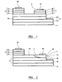
- Figure 1 shows a schematic cross-sectional view of an NPN bipolar transistor comprising a base 1, an emitter 2 and a relatively large collector 3.
- the excluding structure comprises a p + p + junction heterojunction 4.
- the figures in brackets used in relation to this Figure and in Figure 2 refer to carrier concentration.
- Layer 15 is overlaid in turn by a 100 nm thick emitter cap layer 16 of n InP (2x 10 18 ), a 150 nm thick emitter contact layer 17 of n InGaAs (1 x 10 19 ) and a emitter metal contact layer 18.
- Layer 19 is overlaid in turn by a 100 nm thick base cap/contact layer 20 of p InGaAs (2 x 10 19 ), and a base metal contact layer 21.
- a metal contact layer 22 is provided on sub-collector layer 12.
- a comparative device used in the comparisons below is constructed as in Figure 1 above but with the base cap/contact layer 20 and the base contact layer 19 omitted.
- Figure 2 shows a schematic cross-sectional view of an NPN bipolar transistor comprising a base 1, an emitter 2 and a relatively large collector 3.
- the excluding structure comprises a p + p + heterojunction 5.
- Layer 34 is in turn overlaid by a 100 nm thick emitter layer 35 of n InP (4 x 10 17 ), a 100 nm thick emitter cap layer 36 of n InP (2 x 10 18 ), a 150 nm thick emitter contact layer 37 of n InGaAs (1 x 10 19 ) and a metal emitter contact layer 38,
- a metal contact layer 42 is provided on sub-collector layer 12.
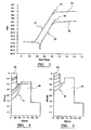
- the device without the excluding contact shows marked thermal runaway as shown by the continued rise in the both base and collector currents at V be - 0.9 V (when the devices are modelled, the current-voltage curves actually have an infinitely steep slope at this point, and it should be noted that the vertical axis is in any case exponential).
- the device of the invention remains stable out to at least 1.5 V as indicated by the portions 55, 56.
- the addition of the base contact greatly reduces the temperature coefficient of the base-emitter junction, allowing stable operation over the whole range of base-emitter voltages.
- the decreased base current necessary for a given collector current also means that the current gain is increased by about 10% in normal operation.
- Figures 4 and 5 are contour plots respectively showing the temperature characteristics of the Figure 1 transistor and the comparative device at a base-emitter voltage V be of 0.9V.
- the temperature of the counters increases in the direction of the arrows A and B respectively.
- the lowest temperature region 60 shown is at about 330° C and the highest temperature region 62 shown is at about 375° C.
- the lowest temperature region 61 shown is at about 325° C and the highest temperature region 62 shown is at about 335° C.
- the comparative device reaches very high temperatures, increasing the chance of device failure and greatly reducing device lifetime.
Landscapes
- Bipolar Transistors (AREA)
- Junction Field-Effect Transistors (AREA)
Abstract
Description
- The present invention relates to bipolar transistors of the kind which implement exclusion and extraction of minority carriers from the base, and in particular to transistors in which the base region has a wide bandgap, i.e. a wide energy gap between the valence band and conduction band.
- The difference in bandgap between the emitter and base regions of a bipolar transistor has a critical effect on current gain, and in determining ƒT (ƒT is the highest frequency at which hfc is above one). A main method of tailoring a band gap difference is to vary the semiconductor composition on one or both sides of a heterojunction.
- Gallium indium arsenide (GaInAs) materials are particularly useful in that they have been demonstrated to provide the highest ƒT of any bipolar transistor. This type of device has been disclosed for example in
EP 0 977 250 -
US 2002/0090789 discloses a heterojunction bipolar transistor (HBT) comprising a collector layer, a base layer of a carbon-doped GaxIn1-xAsySb1-y layer having one surface connected to the collector layer, an emitter layer connected to the other surface of the base layer, a base contact layer of a carbon-doped GaAsSb layer electrically connected to the base layer, and a base electrode formed on the base contact layer. The GaAsSb base contact enables a much reduced base resistance to be obtained and, in consequence, an increased maximum oscillation frequency.EP 0384113 discloses a heterojunction bipolar transistor made with a multilayer layer base which results in low power loss in the base and improved current gain. - As is well known, thermal runaway can occur in bipolar devices when an emitter contact is forward biased. For instance, under constant base-emitter voltage conditions when the current through the device rises, the temperature also rises, reducing the base-emitter turn-on voltage and so enabling the current to rise even further. This type of positive feedback process can lead to damage in the device unless the current is limited in some manner.
- For example, in a multi-finger device, this thermal effect can cause one finger in the device to have a lower turn-on voltage than the others so that substantially all of the collector current flows through the one finger. The gain of the device may be severely affected, and irreversible damage can arise if the condition is allowed to persist. The problem occurs even at constant base current operation.
- A related problem is that hot spots can arise even within one finger, which can similarly cause collapse in the gain and/or burnout. This effect generally occurs only at constant base voltage operation. However, it is increasingly a problem in modem devices with low parasitic base and emitter resistances, where ballasting effects, that is where series resistance damps out instability (see, for example, Liou et al., IEEE Int. Microwave Symp. Dig., 281. (1993)), are absent or greatly reduced.
- The foregoing considerations are particularly relevant for example to mobile communications devices such as telephones, where high power, high frequency signal amplification is required for radio frequency signal transmission.
- Various means of mitigating this problem have been proposed, for example by ensuring that the heat in the device is spread uniformly over the device (see, for example, Bayraktaroglu et al., IEEE Electron Device Letters, 14, 493 (1993)), which however has only a limited effect. A proposal intentionally to incorporate base or collector ballast resistors has the undesirable effect of reducing the gain. The present invention seeks to overcome such limitations.
- The present invention provides a bipolar transistor with a vertical geometry having a base region provided with a base contact, emitter and collector regions arranged to extract minority carriers from the base region, and an excluding heterostructure for counteracting entry of minority carriers into the base region via the base contact, characterised in that the base region has a bandgap of greater than 0.5 eV and a doping lever greater than 1017 cm-3 and in that the excluding heterostructure comprises InP, InGaP, AlGaN, AlGaAs or InAlAs.
- In a transistors with a vertical geometry the separation between the emitter and collector is defined by the growth of the material, and so can be determined to monolayer thickness using molecular beam epitaxy. The transistor of the embodiment has emitter and collector regions on opposed sides of a base layer, and the thinness of the base layer, inter alia, enables high frequency operation, but at the risk of thermal runaway. By contrast, the emitter-collector separation in transistors with a horizontal (or lateral) geometry is determined by lithography. The consequential much greater characteristic length provides much less interaction between emitter and collector and hence a reduced gain, and reduced speed. Characteristically the emitter and collector regions arc spaced laterally on the same side or the base region, as in Fujitsu discussed below.
- An example of a transistor with horizontal geometry is disclosed in
JP 050114602 - For brevity in the description, the structure for counteracting entry of minority carriers into the base via the base contact will henceforth alternatively be termed an excluding structure. An excluding structure acts to accept majority carriers but does not supply minority carriers.
- In a transistor according to the invention the excluding structure may be an excluding heterostructure or heterojunction, with a barrier to prevent carriers entering the base region. A heterostructure comprises materials with different band gaps on either side of the junction, for example in the present case a p+p+ junction, where the underscore indicates a wider band gap than that of the corresponding p layer.
- In an embodiment not according to the invention, the excluding structure may be an implanter region within the base region, providing a "high-low" differentially doped homojunction (semiconductor material with the same bandgap either side of the junction where a dopant concentration alters from one side of the junction to the other) which inhibits minority carrier entry into the base region. Such a structure may be for example a p++p+ junction (the + or ++ refer to overdoping and increased overdoping compared to the same layer type, and conversely and refer to underdoping) which comprise adjacent layers of the same semiconductor material but with different doping or carrier levels. Theoretically at least it would be possible to use different materials with the same bandgap either side of the junction, and with different carrier levels, so that this construction is more generally described as a 'high-low' doping junction. However, there are usually difficulties in matching the lattice constants of different materials.
- The homojunction alternative not only permits simpler fabrication, but also allows the use of a wide gap passivation layer between the base and emitter regions, if desired. Such a passivation layer can improve performance by reducing recombination in the base region, which otherwise causes increased leakage and reduced current gain.
- The transistor may be a high power III-V heterostructure bipolar transistor, preferably a high frequency transistor, for example of indium phosphide and gallium indium arsenide. One particularly suitable form is a transistor laid out in a multi-finger array, i.e. the body of the device is cut into fingers to facilitate heat removal from every part, and the base and emitter contacts are interdigitated so that current may be input and output more easily.
- Particularly where the transistor is based on III-V materials, but not limited to transistors of that type, the emitter may be a heterostructure. No such emitter is disclosed in Fujitsu mentioned above.
- In devices according to the invention thermal runaway is reduced, and they may therefore be operated at higher temperature or higher current. The stability of multi-finger devices may be increased without, for example, resorting to ballast resistors.
- Our copending Application No
WO 01/93337 - Semiconductor materials suitable for use in the invention have a band gap of greater than 0.5 eV, possibly greater than 0.52 eV, or even 0.55 eV or more. While any suitable such material known in the art may be employed, some preferred semiconductor materials are GaAs, indium gallium arsenide (InGaAs), InGaAsSb, GaN, indium phosphide (InP), InGaP, AlGaN, AlGaAs, and InAlAs. In particular GaAs, InGaAs, InGaAsSb and GaN are useful materials for the base region, and in an excluding heterostructure InP, InGaP, AIGaN, AIGaAs and InAlAs are the wide gap materials.
- Transistors according to the invention preferably comprise more than one semiconductor composition with different bandgaps, so providing a heterostructure or heterojunction device. The heterostructure may occur in the base or collector region, for example.
- Adjacent regions with different bandgaps may also have different dopant levels, for example a heterojunction p++p+.
- In a preferred from of transistor according to the invention, the collector region includes a heterostructure. This construction has been found to decrease thermal runaway to an unexpected extent.
- Transistors according to the invention may be fabricated using methods known to the person skilled in the art. Preferably, an excluding structure is formed by using regrowth to grow a p+p+ heterostructure.
- Transistors according to the invention may alternatively be fabricated by leaving the wide bandgap emitter material in place over the extrinsic base after the emitter mesa is etched instead of etching down to the top of the base. The wide bandgap material would then just be etched away under the base contact (to improve contact resistance), and/or the base contact implant used to type convert it to p-type. The wide bandgap region then provides a passivation layer on top of the extrinsic base, which reduces recombination currents in the base, improving current gain.
- While examples of junctions provided in this application relate to NPN bipolar transistors, it should be understood that similar considerations apply for PNP bipolar transistors
- The invention extends to a method of reducing the tendency to thermal runaway in a bipolar transistor with a vertical geometry having a base region provided with a base contact, emitter and collector regions arranged to extract minority carriers from the base region, the base region having a bandgap of greater than 0.5 eV and a doping level greater than 1017 cm·3, by providing an excluding heterostructure for counteracting entry of minority carriers into the base region via the base contact, the excluding heterostructure comprising [nP, InGaP, AlGaN, AlGaAs or InAlAs.
- Further features and advantages of the invention will become clear upon consideration of the appended claims, to which the reader is referred, and upon a reading of the following more detailed description of exemplary embodiments of the invention, made with reference to the accompanying drawings, in which:
-
Figure 1 is a schematic cross-sectional view of a transistor of the invention with an excluding heterostructure; -
Figure 2 is a schematic cross-sectional view of a transistor of the invention with an excluding heterostructure; -
Figure 3 is a graph showing a Gummel plot for the transistor ofFigure 1 and for an equivalent device without the excluding heterostructure; -
Figure 4 shows the thermal characteristics of the transistor ofFigure 1 and -
Figure 5 shows the thermal characteristics of the device of the equivalent device to that ofFigure 1 without the excluding heterostructure. -
Figure 1 shows a schematic cross-sectional view of an NPN bipolar transistor comprising abase 1, anemitter 2 and a relativelylarge collector 3. The excluding structure comprises a p+p+ junction heterojunction 4. The figures in brackets used in relation to this Figure and inFigure 2 refer to carrier concentration. - A 0.3 µm thick
sub-collector layer 12 of n InGaAs (6 x 10¹⁸) and a 0.6µm collector layer 13 of n InGaAs (1 x 10¹⁶) successively overlie asubstrate layer 11 of semiinsulating InP. A 70 nmthick base layer 14 of p InGaAs (1 x 10¹⁹) lies overlayer 13 and different areas thereof are in turn overlaid by a 100 nmthick emitter layer 15 of n InP (4 x 10¹⁷) and a 100 nm thick excludingbase contact layer 19 of p InP (2 x 10¹⁹). -
Layer 15 is overlaid in turn by a 100 nm thick emitter cap layer 16 of n InP (2x 10¹⁸), a 150 nm thickemitter contact layer 17 of n InGaAs (1 x 10¹⁹) and a emittermetal contact layer 18.Layer 19 is overlaid in turn by a 100 nm thick base cap/contact layer 20 of p InGaAs (2 x 10¹⁹), and a basemetal contact layer 21. - A
metal contact layer 22 is provided onsub-collector layer 12. - A comparative device used in the comparisons below is constructed as in
Figure 1 above but with the base cap/contact layer 20 and thebase contact layer 19 omitted. -
Figure 2 shows a schematic cross-sectional view of an NPN bipolar transistor comprising abase 1, anemitter 2 and a relativelylarge collector 3. The excluding structure comprises a p+p+ heterojunction 5. - A 0.3 µm thick
sub-collector layer 32 of n TnGaAs (6 x 10¹⁸) and a 0.6µm collector layer 33 of n InGaAs (1 x 10¹⁶) successively overlie asubstrate layer 31 of semiinsulating InP. A 70 nmthick base layer 34 of p InGaAs (1 x 10¹⁹) lies overlayer 33 but includes a local 100 nm thick region of p InP (2 x 10¹⁹) providing abase excluding contact 40 which carries a metalbase cap layer 41.Layer 34 is in turn overlaid by a 100 nmthick emitter layer 35 of n InP (4 x 10¹⁷), a 100 nm thick emitter cap layer 36 of n InP (2 x 10¹⁸), a 150 nm thickemitter contact layer 37 of n InGaAs (1 x 10¹⁹) and a metal emitter contact layer 38, - A
metal contact layer 42 is provided onsub-collector layer 12. -
Figure 3 illustrates thermal runaway characteristics of the device ofFigure 1 and the comparative device mentioned above, as obtained by 2D thermal/drift-diffusion modelling. It is a Gummel plot of collector and base currents (in amps per micron - 2d simulation) versus base voltage at Vcc = 0.8 V. Theupper part 51 of the plot shows the collector current and thelower part 52 the base current, and it will be seen that the device of the invention, with the excluding structure, permit larger values of current before the onset of thermal runaway. The device without the excluding contact shows marked thermal runaway as shown by the continued rise in the both base and collector currents at Vbe - 0.9 V (when the devices are modelled, the current-voltage curves actually have an infinitely steep slope at this point, and it should be noted that the vertical axis is in any case exponential). In contrast, the device of the invention remains stable out to at least 1.5 V as indicated by theportions - The addition of the base contact greatly reduces the temperature coefficient of the base-emitter junction, allowing stable operation over the whole range of base-emitter voltages. The decreased base current necessary for a given collector current also means that the current gain is increased by about 10% in normal operation.
-
Figures 4 and 5 are contour plots respectively showing the temperature characteristics of theFigure 1 transistor and the comparative device at a base-emitter voltage Vbe of 0.9V. The temperature of the counters increases in the direction of the arrows A and B respectively. InFigure 4 thelowest temperature region 60 shown is at about 330° C and thehighest temperature region 62 shown is at about 375° C. InFigure 5 thelowest temperature region 61 shown is at about 325° C and thehighest temperature region 62 shown is at about 335° C. Thus lower temperature operation of the transistor ofFigure 5 according to the invention is clearly illustrated. It is clear that the comparative device reaches very high temperatures, increasing the chance of device failure and greatly reducing device lifetime.
Claims (11)
- A, bipolar transistor with a vertical geometry having a base region provided with a base contact, emitter and collector regions arranged to extract minority carriers from the base region, and an excluding heterostructure for counteracting entry of minority carriers into the base region via the base contact, characterise in that the base region has a bandgap of greater than 0.5 eV and a doping level greater than 1017 cm-3 and in that the excluding heterostructure comprises InP, InGaP, AIGaN, AIGaAs or InAlAs.
- A transistor according to claim 1 based on III-V materials.
- A transistor according to claim 1 or claim 2 wherein the base region comprises GaAs, InGaAs, InGaAsSb, or GaN.
- A transistor according to any preceding claim wherein the transistor is a high power III-V heterostructure bipolar transistor.
- A transistor according to any preceding claim wherein the transistor is a high frequency transistor.
- A transistor according to any preceding claim wherein the transistor is of a multi-finger array construction.
- A transistor according to any preceding claim wherein said bandgap is greater than 0.52 eV.
- A transistor according to any preceding claim and having a heterostructure emitter region.
- A transistor according to any preceding claim and having a heterostructure collector region.
- A transistor according to claim 8 or 9 wherein the heterostructure region comprises a wide gap material selected from InP, InGaP, AIGaN, AIGaAs and InAlAs.
- A method of reducing the tendency to thermal runaway in a bipolar transistor with a vertical geometry having a base region provided with a base contact, emitter and collector regions arranged to extract minority carriers from the base region, the base region having a bandgap of greater than 0.5 eV and a doping level greater than 1017 cm-3, by providing an excluding heterostructure for counteracting entry of minority carriers into the base region via the base contact, the excluding heterostructure comprising InP, InGaP, AIGaN, AIGaAs or InAIAs.
Applications Claiming Priority (3)
| Application Number | Priority Date | Filing Date | Title |
|---|---|---|---|
| GBGB0200067.7A GB0200067D0 (en) | 2002-01-03 | 2002-01-03 | Wide bandgap transistors |
| GB0200067 | 2002-01-03 | ||
| PCT/GB2002/005904 WO2003056629A1 (en) | 2002-01-03 | 2002-12-23 | Wide bandgap bipolar transistors |
Publications (2)
| Publication Number | Publication Date |
|---|---|
| EP1468450A1 EP1468450A1 (en) | 2004-10-20 |
| EP1468450B1 true EP1468450B1 (en) | 2011-06-15 |
Family
ID=9928573
Family Applications (1)
| Application Number | Title | Priority Date | Filing Date |
|---|---|---|---|
| EP02805835A Expired - Lifetime EP1468450B1 (en) | 2002-01-03 | 2002-12-23 | Wide bandgap bipolar transistors |
Country Status (8)
| Country | Link |
|---|---|
| US (1) | US6989581B2 (en) |
| EP (1) | EP1468450B1 (en) |
| JP (2) | JP2005513814A (en) |
| AT (1) | ATE513314T1 (en) |
| AU (1) | AU2002367213A1 (en) |
| GB (1) | GB0200067D0 (en) |
| TW (1) | TWI269440B (en) |
| WO (1) | WO2003056629A1 (en) |
Family Cites Families (8)
| Publication number | Priority date | Publication date | Assignee | Title |
|---|---|---|---|---|
| US3868720A (en) * | 1973-12-17 | 1975-02-25 | Westinghouse Electric Corp | High frequency bipolar transistor with integral thermally compensated degenerative feedback resistance |
| US4617724A (en) * | 1983-06-30 | 1986-10-21 | Fujitsu Limited | Process for fabricating heterojunction bipolar transistor with low base resistance |
| EP0384113A3 (en) | 1989-02-22 | 1990-10-24 | Motorola, Inc. | Multilayer base heterojunction biopolar transistor |
| JPH05114602A (en) | 1991-10-23 | 1993-05-07 | Fujitsu Ltd | Lateral bipolar transistor |
| JP3156436B2 (en) * | 1993-04-05 | 2001-04-16 | 日本電気株式会社 | Heterojunction bipolar transistor |
| JP3628873B2 (en) | 1998-04-28 | 2005-03-16 | 富士通株式会社 | Semiconductor device and manufacturing method thereof |
| DE19834491A1 (en) * | 1998-07-31 | 2000-02-03 | Daimler Chrysler Ag | Arrangement and method for producing a heterobipolar transistor |
| GB0012925D0 (en) | 2000-05-30 | 2000-07-19 | Secr Defence | Bipolar transistor |
-
2002
- 2002-01-03 GB GBGB0200067.7A patent/GB0200067D0/en not_active Ceased
- 2002-12-23 JP JP2003557046A patent/JP2005513814A/en not_active Withdrawn
- 2002-12-23 AU AU2002367213A patent/AU2002367213A1/en not_active Abandoned
- 2002-12-23 EP EP02805835A patent/EP1468450B1/en not_active Expired - Lifetime
- 2002-12-23 US US10/497,814 patent/US6989581B2/en not_active Expired - Fee Related
- 2002-12-23 AT AT02805835T patent/ATE513314T1/en not_active IP Right Cessation
- 2002-12-23 WO PCT/GB2002/005904 patent/WO2003056629A1/en not_active Ceased
-
2003
- 2003-01-02 TW TW092100031A patent/TWI269440B/en not_active IP Right Cessation
-
2008
- 2008-06-12 JP JP2008154287A patent/JP2008258651A/en not_active Withdrawn
Also Published As
| Publication number | Publication date |
|---|---|
| JP2005513814A (en) | 2005-05-12 |
| TWI269440B (en) | 2006-12-21 |
| JP2008258651A (en) | 2008-10-23 |
| TW200302577A (en) | 2003-08-01 |
| US6989581B2 (en) | 2006-01-24 |
| WO2003056629A1 (en) | 2003-07-10 |
| US20050017266A1 (en) | 2005-01-27 |
| GB0200067D0 (en) | 2002-02-20 |
| EP1468450A1 (en) | 2004-10-20 |
| ATE513314T1 (en) | 2011-07-15 |
| AU2002367213A1 (en) | 2003-07-15 |
Similar Documents
| Publication | Publication Date | Title |
|---|---|---|
| Mondry et al. | Heterojunction bipolar transistor using a (Ga, In) P emitter on a GaAs base, grown by molecular beam epitaxy | |
| US6881988B2 (en) | Heterojunction bipolar transistor and semiconductor integrated circuit device using the same | |
| TW569452B (en) | Method and structure for a heterojunction bipolar transistor | |
| US20030025179A1 (en) | Graded base GaAsSb for high speed GaAs HBT | |
| US5349201A (en) | NPN heterojunction bipolar transistor including antimonide base formed on semi-insulating indium phosphide substrate | |
| US6936871B2 (en) | Heterojunction bipolar transistor with a base layer that contains bismuth | |
| US20020149033A1 (en) | GaN HBT superlattice base structure | |
| US7821037B2 (en) | Heterojunction bipolar transistor | |
| US6768141B2 (en) | Heterojunction bipolar transistor (HBT) having improved emitter-base grading structure | |
| US6806513B2 (en) | Heterojunction bipolar transistor having wide bandgap material in collector | |
| JPWO2006003845A1 (en) | Heterojunction bipolar transistor | |
| US6989581B2 (en) | Wide band gap bipolar transistor with reduced thermal runaway | |
| Ida et al. | Enhancement of f/sub max/in InP/InGaAs HBTs by selective MOCVD growth of heavily-doped extrinsic base regions | |
| Sato et al. | InGaAs/InAlAs/InP collector-up microwave heterojunction bipolar transistors | |
| Yanagihara et al. | 253-GHz f/sub max/AlGaAs/GaAs HBT with Ni/Ti/Pt/Ti/Pt-contact and L-shaped base electrode | |
| Lee et al. | Application of O+ implantation in inverted InGaAs/InAlAs heterojunction bipolar transistors | |
| US20050173730A1 (en) | Collector layer structure for a double hetero-junction bipolar transistor for power amplification applications | |
| Dong et al. | C/sub bc/reduction in InP heterojunction bipolar transistor with selectively implanted collector pedestal | |
| Loga et al. | Fabrication and characterization of circular geometry InGaP/GaAs double heterojunction bipolar transistors | |
| US10818781B2 (en) | Heterojunction bipolar transistor structure with a bandgap graded hole barrier layer | |
| WO2002061821A2 (en) | Method of preparing indium phosphide heterojunction bipolar transistors | |
| Oka et al. | Small InGaP/GaAs heterojunction bipolar transistors with high-speed operation | |
| Loga et al. | Fabrication and characterization of circular geometry InP/InGaAs double heterojunction bipolar transistors | |
| Chung et al. | Current gain dependence on subcollector and etch-stop doping in InGaP/GaAs HBTs | |
| Cui et al. | Comparison of DC and high-frequency performance of zinc-doped and carbon-doped InP/InGaAs HBTs grown by metalorganic chemical vapor deposition |
Legal Events
| Date | Code | Title | Description |
|---|---|---|---|
| PUAI | Public reference made under article 153(3) epc to a published international application that has entered the european phase |
Free format text: ORIGINAL CODE: 0009012 |
|
| 17P | Request for examination filed |
Effective date: 20040526 |
|
| AK | Designated contracting states |
Kind code of ref document: A1 Designated state(s): AT BE BG CH CY CZ DE DK EE ES FI FR GB GR IE IT LI LU MC NL PT SE SI SK TR |
|
| AX | Request for extension of the european patent |
Extension state: AL LT LV MK RO |
|
| 17Q | First examination report despatched |
Effective date: 20100203 |
|
| GRAP | Despatch of communication of intention to grant a patent |
Free format text: ORIGINAL CODE: EPIDOSNIGR1 |
|
| GRAS | Grant fee paid |
Free format text: ORIGINAL CODE: EPIDOSNIGR3 |
|
| GRAA | (expected) grant |
Free format text: ORIGINAL CODE: 0009210 |
|
| AK | Designated contracting states |
Kind code of ref document: B1 Designated state(s): AT BE BG CH CY CZ DE DK EE ES FI FR GB GR IE IT LI LU MC NL PT SE SI SK TR |
|
| REG | Reference to a national code |
Ref country code: GB Ref legal event code: FG4D Ref country code: CH Ref legal event code: EP |
|
| REG | Reference to a national code |
Ref country code: IE Ref legal event code: FG4D |
|
| REG | Reference to a national code |
Ref country code: DE Ref legal event code: R096 Ref document number: 60240306 Country of ref document: DE Effective date: 20110721 |
|
| REG | Reference to a national code |
Ref country code: NL Ref legal event code: VDEP Effective date: 20110615 |
|
| PG25 | Lapsed in a contracting state [announced via postgrant information from national office to epo] |
Ref country code: SE Free format text: LAPSE BECAUSE OF FAILURE TO SUBMIT A TRANSLATION OF THE DESCRIPTION OR TO PAY THE FEE WITHIN THE PRESCRIBED TIME-LIMIT Effective date: 20110615 |
|
| PG25 | Lapsed in a contracting state [announced via postgrant information from national office to epo] |
Ref country code: FI Free format text: LAPSE BECAUSE OF FAILURE TO SUBMIT A TRANSLATION OF THE DESCRIPTION OR TO PAY THE FEE WITHIN THE PRESCRIBED TIME-LIMIT Effective date: 20110615 Ref country code: AT Free format text: LAPSE BECAUSE OF FAILURE TO SUBMIT A TRANSLATION OF THE DESCRIPTION OR TO PAY THE FEE WITHIN THE PRESCRIBED TIME-LIMIT Effective date: 20110615 Ref country code: SI Free format text: LAPSE BECAUSE OF FAILURE TO SUBMIT A TRANSLATION OF THE DESCRIPTION OR TO PAY THE FEE WITHIN THE PRESCRIBED TIME-LIMIT Effective date: 20110615 Ref country code: CY Free format text: LAPSE BECAUSE OF FAILURE TO SUBMIT A TRANSLATION OF THE DESCRIPTION OR TO PAY THE FEE WITHIN THE PRESCRIBED TIME-LIMIT Effective date: 20110615 Ref country code: GR Free format text: LAPSE BECAUSE OF FAILURE TO SUBMIT A TRANSLATION OF THE DESCRIPTION OR TO PAY THE FEE WITHIN THE PRESCRIBED TIME-LIMIT Effective date: 20110916 |
|
| PG25 | Lapsed in a contracting state [announced via postgrant information from national office to epo] |
Ref country code: NL Free format text: LAPSE BECAUSE OF FAILURE TO SUBMIT A TRANSLATION OF THE DESCRIPTION OR TO PAY THE FEE WITHIN THE PRESCRIBED TIME-LIMIT Effective date: 20110615 Ref country code: BE Free format text: LAPSE BECAUSE OF FAILURE TO SUBMIT A TRANSLATION OF THE DESCRIPTION OR TO PAY THE FEE WITHIN THE PRESCRIBED TIME-LIMIT Effective date: 20110615 |
|
| PG25 | Lapsed in a contracting state [announced via postgrant information from national office to epo] |
Ref country code: CZ Free format text: LAPSE BECAUSE OF FAILURE TO SUBMIT A TRANSLATION OF THE DESCRIPTION OR TO PAY THE FEE WITHIN THE PRESCRIBED TIME-LIMIT Effective date: 20110615 Ref country code: PT Free format text: LAPSE BECAUSE OF FAILURE TO SUBMIT A TRANSLATION OF THE DESCRIPTION OR TO PAY THE FEE WITHIN THE PRESCRIBED TIME-LIMIT Effective date: 20111017 Ref country code: EE Free format text: LAPSE BECAUSE OF FAILURE TO SUBMIT A TRANSLATION OF THE DESCRIPTION OR TO PAY THE FEE WITHIN THE PRESCRIBED TIME-LIMIT Effective date: 20110615 |
|
| PG25 | Lapsed in a contracting state [announced via postgrant information from national office to epo] |
Ref country code: SK Free format text: LAPSE BECAUSE OF FAILURE TO SUBMIT A TRANSLATION OF THE DESCRIPTION OR TO PAY THE FEE WITHIN THE PRESCRIBED TIME-LIMIT Effective date: 20110615 |
|
| PLBE | No opposition filed within time limit |
Free format text: ORIGINAL CODE: 0009261 |
|
| STAA | Information on the status of an ep patent application or granted ep patent |
Free format text: STATUS: NO OPPOSITION FILED WITHIN TIME LIMIT |
|
| 26N | No opposition filed |
Effective date: 20120316 |
|
| PG25 | Lapsed in a contracting state [announced via postgrant information from national office to epo] |
Ref country code: IT Free format text: LAPSE BECAUSE OF FAILURE TO SUBMIT A TRANSLATION OF THE DESCRIPTION OR TO PAY THE FEE WITHIN THE PRESCRIBED TIME-LIMIT Effective date: 20110615 |
|
| PG25 | Lapsed in a contracting state [announced via postgrant information from national office to epo] |
Ref country code: DK Free format text: LAPSE BECAUSE OF FAILURE TO SUBMIT A TRANSLATION OF THE DESCRIPTION OR TO PAY THE FEE WITHIN THE PRESCRIBED TIME-LIMIT Effective date: 20110615 |
|
| REG | Reference to a national code |
Ref country code: DE Ref legal event code: R097 Ref document number: 60240306 Country of ref document: DE Effective date: 20120316 |
|
| PG25 | Lapsed in a contracting state [announced via postgrant information from national office to epo] |
Ref country code: MC Free format text: LAPSE BECAUSE OF NON-PAYMENT OF DUE FEES Effective date: 20111231 |
|
| REG | Reference to a national code |
Ref country code: CH Ref legal event code: PL |
|
| REG | Reference to a national code |
Ref country code: IE Ref legal event code: MM4A |
|
| PG25 | Lapsed in a contracting state [announced via postgrant information from national office to epo] |
Ref country code: LI Free format text: LAPSE BECAUSE OF NON-PAYMENT OF DUE FEES Effective date: 20111231 Ref country code: IE Free format text: LAPSE BECAUSE OF NON-PAYMENT OF DUE FEES Effective date: 20111223 Ref country code: CH Free format text: LAPSE BECAUSE OF NON-PAYMENT OF DUE FEES Effective date: 20111231 |
|
| PG25 | Lapsed in a contracting state [announced via postgrant information from national office to epo] |
Ref country code: ES Free format text: LAPSE BECAUSE OF FAILURE TO SUBMIT A TRANSLATION OF THE DESCRIPTION OR TO PAY THE FEE WITHIN THE PRESCRIBED TIME-LIMIT Effective date: 20110926 |
|
| PGFP | Annual fee paid to national office [announced via postgrant information from national office to epo] |
Ref country code: DE Payment date: 20121220 Year of fee payment: 11 Ref country code: FR Payment date: 20130130 Year of fee payment: 11 |
|
| PG25 | Lapsed in a contracting state [announced via postgrant information from national office to epo] |
Ref country code: LU Free format text: LAPSE BECAUSE OF NON-PAYMENT OF DUE FEES Effective date: 20111223 |
|
| PG25 | Lapsed in a contracting state [announced via postgrant information from national office to epo] |
Ref country code: BG Free format text: LAPSE BECAUSE OF FAILURE TO SUBMIT A TRANSLATION OF THE DESCRIPTION OR TO PAY THE FEE WITHIN THE PRESCRIBED TIME-LIMIT Effective date: 20110915 |
|
| PG25 | Lapsed in a contracting state [announced via postgrant information from national office to epo] |
Ref country code: TR Free format text: LAPSE BECAUSE OF FAILURE TO SUBMIT A TRANSLATION OF THE DESCRIPTION OR TO PAY THE FEE WITHIN THE PRESCRIBED TIME-LIMIT Effective date: 20110615 |
|
| REG | Reference to a national code |
Ref country code: DE Ref legal event code: R119 Ref document number: 60240306 Country of ref document: DE |
|
| PGFP | Annual fee paid to national office [announced via postgrant information from national office to epo] |
Ref country code: GB Payment date: 20140521 Year of fee payment: 12 |
|
| REG | Reference to a national code |
Ref country code: DE Ref legal event code: R119 Ref document number: 60240306 Country of ref document: DE Effective date: 20140701 |
|
| REG | Reference to a national code |
Ref country code: FR Ref legal event code: ST Effective date: 20140829 |
|
| PG25 | Lapsed in a contracting state [announced via postgrant information from national office to epo] |
Ref country code: DE Free format text: LAPSE BECAUSE OF NON-PAYMENT OF DUE FEES Effective date: 20140701 |
|
| PG25 | Lapsed in a contracting state [announced via postgrant information from national office to epo] |
Ref country code: FR Free format text: LAPSE BECAUSE OF NON-PAYMENT OF DUE FEES Effective date: 20131231 |
|
| GBPC | Gb: european patent ceased through non-payment of renewal fee |
Effective date: 20141223 |
|
| PG25 | Lapsed in a contracting state [announced via postgrant information from national office to epo] |
Ref country code: GB Free format text: LAPSE BECAUSE OF NON-PAYMENT OF DUE FEES Effective date: 20141223 |