BACKGROUND OF THE INVENTION
Field of the Invention
The present invention relates to a light emitting display
panel in which for example an organic EL (electroluminescent)
element is employed as a light emitting element, and particularly
to a drive method and a drive device of a passive drive type
light emitting display panel in which an excellent gradation
expression can be realized without subdividing intensity
resolution so much in the case where time gradation is
implemented.
Description of the Related Art
A display panel which is constructed by arranging light
emitting elements in a matrix pattern has been developed widely,
and as the light emitting element employed in such a display
panel, an organic EL element in which an organic material is
employed in a light emitting layer has attracted attention. This
is because of backgrounds one of which is that by employing,
in the light emitting layer of the element, an organic compound
which enables an excellent light emitting characteristic to be
expected, a high efficiency and a long life have been achieved
which make an EL element satisfactorily practicable.
The organic EL element can be electrically represented
by an equivalent circuit as shown in FIG. 1. That is, the organic
EL element can be replaced by a structure composed of a diode
element E and a parasitic capacitance element Cp which is coupled
in parallel to this diode element, and the organic EL element
has been considered as a capacitor like light emitting element.
When a light emission driving voltage is applied to this organic
EL element, at first, electrical charges corresponding to the
electric capacity of this element flow into an electrode as a
displacement current and are accumulated. Then, it can be
considered that when the voltage exceeds a determined voltage
( light emission threshold voltage = Vth) peculiar to the element
in question, current begins to flow from the electrode (anode
side of the diode element E) to an organic layer constituting
the light emitting layer so that the element emits light at an
intensity proportional to this current.
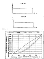
FIG. 2 shows light emission static characteristics of such
organic EL element. According to these, the organic EL element
emits light at an intensity (L) approximately proportional to
drive current (I) as shown in FIG. 2A and emits light while current
(I) flows drastically when the drive voltage (V) is the light
emission threshold voltage (Vth) or higher as shown in FIG. 2B.
In other words, when the drive voltage is the light emission
threshold voltage (Vth) or lower, current rarely flows in the
EL element, and the EL element does not emit light. Therefore,
the EL element has an intensity characteristic that in a light
emission possible region in which the voltage is higher than
the threshold voltage (Vth), the greater the value of the voltage
(V) applied to the EL element becomes, the higher the light
emission intensity (L) of the EL element becomes as shown by
the solid line in FIG. 2C.
It has been known that the intensity property of the organic
EL element changes due to temperature changes approximately as
shown by broken lines in FIG. 2C. That is, while the EL element
has a characteristic that the greater the value of the voltage
(V) applied thereto, the higher the light emission intensity
(L) thereof in the light emission possible region in which the
voltage is higher than the light emission threshold voltage as
described above, the EL element also has a characteristic that
the higher the temperature becomes, the lower the light emission
threshold voltage becomes. Accordingly, the EL element becomes
in a state where light emission of the EL element is possible
by a lower applied voltage as the temperature becomes higher,
and thus the EL element has a temperature dependency of the
intensity that the EL element is brighter at a high temperature
and is darker at a lower temperature though the same light emission
possible voltage is applied.
In general, a constant current drive is performed for the
organic EL element due to the reason that the voltage vs. intensity
characteristic is unstable with respect to temperature changes
as described above while the current vs. intensity characteristic
is stable with respect to temperature changes, the reason that
the organic EL element is drastically deteriorated by an excess
current, and the like. As a display panel employing such organic
EL elements, a passive drive type display panel in which the
elements are arranged in a matrix pattern has been put into
practical use already.
As described above, since the organic EL element is a
capacitor like load, while the constant current drive is merely
performed, a rising of the voltage between both ends of the element,
that is, a rising of light emission, is not fast. Particularly,
in the display panel by the passive drive method, since an light
emission operation of the EL element is performed in an instant
only at the time of scan, making the ratio of light emittable
time during a scan period as great as possible by making the
rising of light emission as steep as possible has been considered.
As means for making the rising of light emission of the
EL element as steep as possible, some methods have been known
such as a cathode reset method (e.g., refer to Patent document
1) in which the parasitic capacitance element is charged from
the cathode side of the element by rush current, a constant current
charge method (e.g., refer to Patent document 2) in which the
parasitic capacitance element is charged from the anode side
of the element by a large amount of current, a constant voltage
charge method (e.g., refer to Patent document 2) in which the
parasitic capacitance element of the element is charged from
a constant voltage source, and the like.
[Patent document 1]
Japanese Patent Application Laid-Open No. H9-232074
(paragraphs 0018 to 0034 and FIGS. 1 to 4)
[Patent document 2]
Japanese Patent Application Laid-Open No. 2001-331149
(paragraphs 0015 to 0026 and FIGS. 1 to 3)
[Patent document 3]
Japanese Patent Application Laid-Open No. H11-231834
(paragraphs 0027 to 0032 and FIGS. 1 to 3)
Meanwhile, in the case where a charging means for the
capacitance element as described above is adopted, the time
required for emitting light in an EL element is shortened, and
generally a light emission response characteristic has a
rectangular or spike-like rising as shown in FIGS. 3A, 3B. That
is, the horizontal axes in FIG. 3 represent the lighting period
(lighting progress time t) of the element in the scan period
of one line, and the vertical axes represent the light emission
intensity (L). For example, in the case where the
above-mentioned cathode reset method is adopted, the charging
operation for the parasitic capacitance of an EL element which
will be a next scan lighting object is implemented by rush current
via respective parasitic capacitances in the parallel state of
the other EL elements which will not be the scan lighting object.
In this case, in general, since this charging operation is
implemented utilizing a reverse bias voltage VM which is higher
than a forward voltage Vf of an EL element in a lighting state,
the rising of the lighting is the spike-like rising as shown
in FIG. 3B. In the case where the gradation expression is
implemented in a display panel of this type, time gradation which
controls a light emission time can be utilized suitably. In
this time gradation expression, when a PWM (pulse width
modulation) gradation method is utilized, the gradation (PWM
time) vs. intensity characteristic becomes the time integral
of the light emission response waveform shown in FIG. 3.
Accordingly, in the case of control in which PWM is equally divided
by the rectangular light emission drive as shown in FIG. 3A,
a characteristic in which gradation is linear is obtained.
However, an ideal gradation vs. intensity characteristic
is supposed to be a gamma curve in which gamma (visual degree)
= approximately 1.8 to 2.2 as shown in FIG. 4. Accordingly,
it is necessary to make the intensity difference between
gradations small in a low gradation side and to make it large
in a high gradation side. The minimum intensity resolution in
the gamma curve corresponds to the intensity difference between
the 0th gradation and the first gradation. Accordingly, in the
case where one tries to obtain a gamma characteristic by the
rectangular light emission drive as shown in FIG. 3A, it is
necessary to make a PWM resolution of a low gradation side small.
Table 1 shows results of calculation of how large minimum PWM
resolution is necessary taking a 16 step gradation display of
the rectangular light emission drive as an example.
| | linear | γ = 1.8 | γ = 2.0 | γ = 2.2 |
| Time resolution (when PWM 100% is treated as 1) | 0.067 | 0.008 | 0.004 | 0.003 |
| Minimum resolution magnification (for gamma = 1) | 1.000 | 8.727 | 15.000 | 25.782 |
According to Table 1, for example, when gamma = 2.0 is
to be obtained, it is shown that 15 times of resolution is necessary
for linear gradation. This corresponds to the case of the
rectangular light emission drive as shown in FIG. 3A.
Particularly when the rising of the light emission is spike-like
as shown in FIG. 3B, it is obvious that a resolution smaller
than that of the rectangular light emission drive is necessary.
In sum, in a drive in which the light emission response
is rectangular or spike-like as shown in FIG. 3, in order to
obtain a gamma characteristic, it is necessary to make the
resolution small. In other words, a faster clock signal is
necessary in order to make the resolution small. At the same
time, the EL element has a temperature dependency as described
based on FIG. 2C, and therefore changes in the light emission
rising depending on temperature largely influences the gamma
characteristic.
SUMMARY OF THE INVENTION
The present invention has been developed as attention to
the above-described problems has been paid, and it is an object
of the present invention to provide a drive method and a drive
device for a passive drive type light emitting display panel
by which an excellent gradation expression can be realized
without subdividing intensity resolution so much in the case
where the above-mentioned time gradation is performed.
A drive method of a light emitting display panel according
to the present invention which has been developed in order to
carry out the object described above is, as described in a first
aspect, a drive method of a light emitting display panel in which
light emitting elements are connected at respective crossing
points between a plurality of data lines and a plurality of scan
lines so that the light emitting elements connected to the
respective scan lines are sequentially selectively lighted by
sequentially scanning the scan lines, characterized in that
provided is at least one of an intensity increase period in which
a light emission intensity of the light emitting element is
gradually increased allowing the light emission intensity to
reach a constant intensity state within a predetermined period
from a scan start in one scan period or an intensity decrease
period in which the light emission intensity of the light emitting
element is gradually decreased from the constant intensity state
within a predetermined period which is immediately before the
completion of the scan period.
A drive device of a light emitting display panel according
to the present invention which has been developed in order to
carry out the object described above is, as described in a tenth
aspect, a drive device of a light emitting display panel of a
passive drive system in which light emitting elements are
connected at respective crossing points between a plurality of
data lines and a plurality of scan lines so that the light emitting
elements connected to the respective scan lines are sequentially
selectively lighted by sequentially scanning the scan lines,
characterized in that provided is at least one of an intensity
increase period in which a light emission intensity of the light
emitting element is gradually increased allowing the light
emission intensity to reach a constant intensity state within
a predetermined period from a scan start in one scan period or
an intensity decrease period in which the light emission
intensity of the light emitting element is gradually decreased
from the constant intensity state within a predetermined period
which is immediately before the completion of the scan period.
BRIEF DESCRIPTION OF THE DRAWINGS
FIG. 1 is an equivalent circuit diagram showing the
electrical structure of an organic EL element.
FIGS. 2A, 2B and 2C are characteristic graphs explaining
electrical static characteristics of the organic EL element.
FIGS. 3A and 3B are characteristic graphs explaining light
emission response characteristics adopted in a conventional
drive method.
FIG. 4 is a characteristic graph explaining the
relationship between the gradation and the light emission
intensity.
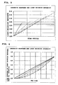
FIG. 5 is a characteristic graph showing an example of
light emission responses in a scan period.
FIG. 6 is a characteristic graph showing an example of
increases of intensities corresponding to the light emission
responses shown in FIG. 5.
FIG. 7 is a characteristic graph for explaining drive
methods according to the present invention.
FIG. 8 is a connection diagram showing a first embodiment
in which a drive method according to the present invention is
utilized.
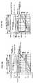
FIGS . 9A and 9B are timing diagrams explaining operations
in the structure shown in FIG. 8.
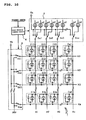
FIG. 10 is a connection diagram showing a second embodiment
in which a drive method according to the present invention is
utilized.
FIG. 11 is timing diagrams explaining operations in the
structure shown in FIG. 10.
DESCRIPTION OF THE PREFERRED EMBODIMENTS
A drive device of a light emitting display panel in which
the present invention is utilized will be described below based
on preferred embodiments thereof. However, a basic concept of
the present invention will be described before it with reference
to FIGS. 5 to 7. First, FIG. 5 shows cases where intensity
increase periods are 0 to 100% of a scan period and shows results
of rough estimates for the relationships of gradations to
intensities. The intensity can be found by time integral
calculus for the light emission response, and results thereof
are shown in FIG. 6. Respective solid line (bold line), solid
line (thin line), broken line (bold line), broken line (thin
line), alternate long and short dash line, and alternate long
and two short dashes line shown in FIG. 5 correspond to respective
those shown in FIG. 6.
As shown by, for example, the alternate long and short
dash line and the alternate long and two short dashes line in
FIG. 5, the longer the intensity increase period within the scan
period, the more moderate intensity increase is shown in a low
PWM region as shown in FIG. 6. That is, the light emission
intensity of a light emitting element can have the characteristic
as the gamma curve described based on FIG. 4. As a result, a
minimum time resolution can be set largely, and it becomes
unnecessary to increase the clock speed. Although the example
shown in FIG. 5 shows the case where the intensity increases,
in the case where the intensity decreases, a gradation
characteristic approximating a reverse gamma curve can be
expected, and in this case also a minimum time resolution can
be set similarly largely, whereby it becomes unnecessary to
increase the clock speed.
In sum, as shown in FIG. 7, within a predetermined period
from a scan start in one scan period, by allowing the light emission
intensity of a light emitting element to increase gradually so
as to allow it to have an intensity increase period reaching
to a constant intensity state, when this is integrated, this
can be allowed to have a gradation characteristic as a gamma
curve. Also, by allowing the light emission intensity of the
light emitting element to have an intensity decrease period in
which this is decreased gradually from the constant intensity
state within a predetermined period immediately before the end
of a scan period as shown in FIG. 7, when this is integrated,
this can be allowed to have a gradation characteristic
approximating a reverse gamma curve.
Thus, as shown in FIG. 7, a drive method of a light emitting
display panel according to the present invention is characterized
by adopting at least either one of setting an intensity increase
period at a scan start time in one scan period or setting an
intensity decrease period immediately before the end of a scan
period. Thus, in the case where a time gradation is realized
as described above, the minimum time resolution can be set largely,
and it becomes unnecessary to increase the clock speed.
FIG. 8 shows a passive drive type display panel developed
based on the above-described technical concept and a first
embodiment of a drive device thereof. Operations thereof based
on the embodiment shown in FIG. 8 will be described with reference
to an example in which the intensity increase period is set at
a scan start time in one scan period. There are two methods
that are a cathode ray scan/anode ray drive and an anode ray
scan/cathode ray drive in drive methods for organic EL elements
in the passive drive type drive system, and the example shown
in FIG. 8 shows the feature of the former cathode ray scan/anode
ray drive.
That is, anode rays A1 to An as n data lines are arranged
in a vertical direction, cathode rays K1 to Km as m scan lines
are arranged in a horizontal direction, and organic EL elements
E11 to Enm as light emitting elements are arranged at portions
at which respective rays intersect each other (in total, nxm
portions) to constitute a display panel 1.
One ends (anode terminals in equivalent diodes of the EL
elements) and other ends (cathode terminals in the equivalent
diodes of the EL elements) of the respective EL elements E11
to Enm constituting pixels are connected to the anode rays and
cathode rays, respectively, corresponding to respective
crossing positions between the anode rays A1 to An extending
along the vertical direction and the cathode rays K1 to Km
extending along the horizontal direction. Further, the
respective anode rays A1 to An are connected to an anode ray
drive circuit 2, and the respective cathode rays K1 to Km are
connected to a cathode ray scan circuit 3, so as to be driven,
respectively.
The anode ray drive circuit 2 is provided with respective
constant current sources cc1 and drive switches Sa1 to San
supplying drive current to the respective EL elements via the
respective anode rays A1 to An. The drive switches Sa1 to San
are connected to the respective constant current sources cc1
sides and are controlled so that current from the constant current
sources cc1 is supplied to the respective EL elements E11 to
Enm arranged corresponding to the cathode rays. The drive
switches Sa1 to San are constructed so that the anode rays are
selectively connected to a voltage source Va or a reference
potential (a ground potential) as described later.
The cathode ray scan circuit 3 is provided with scan
switches Sk1 to Skm corresponding to the respective cathode rays
K1 to Km and operates so as to allow either one of a voltage
source Vk or the ground potential as a scan reference potential
to be connected to corresponding cathode rays. Thus, by
connecting the constant current sources cc1 to desired anode
rays A1 to An while the cathode rays are set at the scan reference
potential (ground potential) at a predetermined cycle, light
of the respective EL elements are selectively emitted.
The anode ray drive circuit 2 and the cathode ray scan
circuit 3 receive commands from a light emission control circuit
4 and operate so as to display an image corresponding to image
data, in response to said image data supplied to the light emission
control circuit. In this case, the cathode ray scan circuit
3 sequentially selects one of the cathode rays corresponding
to the horizontal scan period of the image data by a command
from the light emission control circuit to set it to the ground
potential as the scan reference potential and sequentially
switches the scan switches Sk1 to Skm so that the voltage of
the voltage source Vk is applied to other cathode rays. The
state shown in FIG. 8 shows a state in which the second cathode
ray K2 is scanned and in which the voltage of the voltage source
Vk is applied to the other cathode rays.
A drive control signal for controlling any one of the EL
elements connected to the cathode rays as to which timing and
how long period of time light emission is performed based on
pixel information that the image data shows is supplied from
the light emission control circuit 4 to the anode ray drive circuit
2. The anode ray drive circuit 2 instantaneously connects some
of the drive switches Sa1 to San to the voltage source Va and
connects them to the constant current sources cc 1 sides to control
them in response to the drive control signal so as to supply
drive current to EL elements corresponding to the pixel data
via the anode rays A1 to An.
FIG. 9A is a timing diagram explaining lighting control
for the display panel operated through the first embodiment shown
in FIG. 8. In this FIG. 9A, the horizontal axis shows one line
of scan period in one cathode ray. Reference numeral 1 in the
drawing shows the applied voltage for the EL elements, and
reference numeral 2 shows a light emission response
characteristic of the EL element, that is, the light emission
intensity. Further, reference numeral 3 shows the time integral
value of the light emission response characteristic of the EL
element shown as 2, and reference numeral 4 shows an ideal gamma
curve.
In the embodiment shown in FIG. 8, as shown in FIG. 9A,
the voltage value of the voltage source Va supplied to the anode
ray drive circuit 2 is set to a voltage lower than a forward
voltage Vf in the light emission state (the constant intensity
period) of the EL element or the above-mentioned lighting
threshold voltage Vth. The voltage value of the voltage source
Vk utilized in the cathode ray scan circuit 3 is set to a voltage
higher than the forward voltage Vf.
In the embodiment shown in FIG. 8, one means of the
above-mentioned cathode reset method is adopted in the lighting
control therefor. Here, one means of this cathode reset method
is called a voltage setting means. As shown in FIG. 9A, at a
beginning of one line scan period, the voltage of the voltage
source Va is supplied to the anodes of the EL elements that are
to be scan light emission objects via the anode rays. That is,
the drive switches Sa1 to San in the anode ray drive circuit
2 are connected to the voltage source Va side.
The voltage from the voltage source Vk is supplied to the
cathodes of the EL elements. That is, the scan switches Sk1
to Skm in the cathode ray scan circuit 3 are connected to the
voltage source Vk side. Accordingly, in this state, the voltage
of "Va-Vk" is applied to the EL elements as shown as 1 in FIG.
9A.
Thereafter, the drive switches Sa1 to San of the anode
rays corresponding to EL elements whose lights are to be emitted
are connected to the constant current sources cc1 side, and the
cathode ray of the scan object is connected to the ground potential.
As a result, electrical charges of non-scan line capacitances
(usually, satisfactorily larger than capacitance components of
a scan selected ray) connected to anode rays are concentrated
(rush current) in the scan selected ray. As a result, the anode
potentials become approximately the potential of Va by acceptance
and delivery of electrical charges. That is, in a first set
period of the scan period, setting is performed so that voltage
between both ends of the EL element becomes approximately Va.
Thus, current from the constant current sources cc1 is
supplied to EL elements that are to be the light emission objects,
taking the anode side voltage Va as a starting point to enter
a PWM period. In this PWM period since the EL element is driven
by a constant current, the anode potential thereof shown by 1
is gradually raised and reaches the forward voltage Vf. Then,
the EL element is driven by the constant current and shifts while
still being the forward voltage Vf. As a result, an intensity
increase period in which the light emission response of the EL
element moderately increases as shown by 2 can be provided.
As already described, in the PWM gradation method, the
relationship between the PWM time and the intensity is found
by the time integral of the light emission response shown by
2 as shown by 3. Accordingly, PWM periods of respective
gradations can be set by the time integral of the light emission
response shown by 3. Therefore, by selecting the PWM periods
of the respective gradations, in other words, by setting the
drive switches Sa1 to San shown in FIG. 8 to the ground potential
side in response to a gradation expression, the light emission
time of an EL element can be controlled, and a gradation expression
by the PWM gradation method can be realized.
The PWM periods of the respective gradations shown in FIG.
9A are set based on the light emission response characteristic
shown by 2, and in the case where a further ideal gamma curve
is sought, it is desired that the PWM time is adjusted on the
time axis for each gradation by calculating back from an intensity
value of the ideal gamma curve shown by 4. Thus, a gradation
corresponding to the ideal gamma curve can be obtained.
Meanwhile, FIG. 9B illustrates PWM periods of respective
gradations performed in a conventional example having a light
emission characteristic as shown in FIG. 3 which has already
been described. Respective characteristics shown by 1 to 4 in
FIG. 9B are similar to those described in FIG. 9A. That is,
in the conventional method, the relationship between the anode
side voltage Va and the forward voltage Vf is set to Va ≥ Vf,
and therefore the rising of light emission of an EL element is
rectangular or spike-like.
Therefore, in the case where PWM periods of respective
gradations are set based on the light emission response shown
by 2 in FIG. 9B where the rising of light emission is spick-like,
an extremely small PWM resolution is needed in a low gradation
side. Thus, in order to realize this resolution, the operation
clock has to be increased considerably, which is a problem.
Next, FIG. 10 shows a second embodiment of a drive device
according to the present invention. In FIG. 10, parts
corresponding to the respective constituent parts shown in FIG.
8 which has already been described are shown by the same reference
numerals, and thus detailed explanation thereof will be omitted.
Operations thereof based on the embodiment shown in FIG. 10 will
be described in accordance with an example in which an intensity
increase period is set at a scan start time within one scan period.
In this embodiment shown in FIG. 10, respective first
constant current sources cc1 for the light emission risings of
EL elements and second constant current sources cc2 for
performing the light emission in a constant intensity state are
provided in the anode ray drive circuit 2. Further, the voltage
value of the voltage source Va supplied to the anode ray drive
circuit 2 is set at a voltage lower than the above-mentioned
lighting threshold voltage Vth. The voltage value of the voltage
source Vk utilized in the cathode ray scan circuit 3 is set at
a voltage higher than the forward voltage Vf.
FIG. 11 is for explaining lighting control of the display
panel performed by the second embodiment shown in FIG. 10. That
is, FIG. 11A is for explaining the circumstances of the light
emission rising of an EL element performed first in each one
line scan period, and FIG. 11B is a timing diagram explaining
the lighting control for the display panel. In FIG. 11B,
similarly to the example shown in FIG. 9, the horizontal axis
thereof shows one line of scan period in one cathode ray. The
timing diagram shown in FIG. 11A explains a charging operation
for an element at a beginning of one line scan period in FIG.
11B, that is, the part enclosed by broken lines.
In FIG. 11B, similarly to the example shown in FIG. 9,
reference numeral 1 shows the applied voltage for the EL element,
and 2 shows a light emission response characteristic of the EL
element, that is, the light emission intensity. Further, 3 shows
the time integral value of the light emission response
characteristic of the EL element shown as the 2, and 4 shows
an ideal gamma curve.
In this embodiment, for the time of scan of one line, the
drive switches Sa1 to San have already been connected to the
voltage source Va at a scan finishing time of a line before said
line. A scan cathode ray is connected to the ground potential,
and non-scan cathode rays are connected to the voltage source
Vk. Thus, at a beginning of one line of scan, as shown in FIGS.
11A, 11B, the applied voltage to the respective EL elements that
are to be scanned are allowed to be Va. That is, in the set
period that is a beginning of the scan period, the voltage of
both ends of the EL element is set to approximately Va, and here
they function as a voltage setting means for setting the both
end voltage of the EL element to a constant voltage value.
Then, the drive switches Sa1 to San are connected to the
first constant current sources cc1 sides which are for light
emission rising.
Here, FIG. 11A shows an equivalent circuit regarding one
anode ray at this time, meaning a structure in which one EL element
to be a scan object for the constant current source cc1 and a
plurality of EL elements to be non-scan objects are connected
in parallel and in which n parasitic capacitances C in total
are connected. Charging operation is performed through the
constant current source cc1 for the parasitic capacitances of
the respective EL elements. At this time electrical charges
corresponding to Va have already been charged in the parasitic
capacitances C of the respective EL elements as described above.
The applied voltage for the EL element rises from the Va, having
the current characteristic of cc1 = nc (dV/dt), and in the period
of t1 in which the constant current source cc1 is connected,
the applied voltage to the EL elements increases to Va'.
In this case, a middle level of current which can be roughly
estimated from the capacitance value of the EL element is poured
for a relatively long period of time. Current by which the anode
voltage at the time of completion of t1 time becomes approximately
Vf is desired. Thus, an intensity increase period in which the
light emission response moderately increases as shown as 2 can
be provided. The drive switches Sa1 to San are connected to
the second constant current sources cc2 side after the completion
of the t1 time, and thus the EL element emits light in the constant
intensity state.
The reference numeral 3 in FIG. 11B is the time integral
of the light emission response shown by 2, and thus the PWM periods
of the respective gradations can be set. The drive switches
Sa1 to San shown in FIG. 10 are set to the Va side in response
to a gradation expression so that the light emission time of
the EL element can be controlled, and a gradation expression
by the PWM gradation method can be realized. As described based
on FIG. 9, in the case where an ideal gamma curve is desired
to be obtained, the PWM time can be adjusted on the time axis
for each gradation by calculating back from an intensity value
of the ideal gamma curve shown by 4, and thus a gradation
corresponding to the ideal gamma curve can be obtained.
In the embodiment shown in FIG. 10, although the terminal
voltages of EL elements are increased utilizing the constant
current sources cc1 at a beginning of one scan period, a constant
voltage source by which voltage gradually increases in the
intensity increase period may be employed instead of the constant
current source cc1. Even in the structure in which such constant
voltage source is used, the intensity increase period can be
formed at a beginning of one scan period, and similar interactions
and effects can be obtained.
In this case, it is desired that the applied voltage to
the light emitting element at the time of completion of the
intensity increase period is set at a voltage value which is
approximately equal to the forward voltage Vf of the light
emitting element in the constant intensity state. By setting
like this, the applied voltage of the EL element can be prevented
being given a steep change, and therefore a small PWM resolution
becomes unnecessary.
Although not particularly explained in the
above-described embodiments, when a color display panel is
employed as the display panel, it is desired to construct the
first embodiment shown in FIG. 8 so that through at least one
of the voltage source Va, the PWM time, and the current value
of the constant current sources cc1, a drive operation which
differs depending on respective colors can be performed.
In the case where a color display panel is adopted as the
display panel, it is desired to construct the second embodiment
shown in FIG. 10 so that through at least one of the voltage
value of the voltage source Va, the respective current values
of the constant current sources cc1 and cc2, time t1, and the
PWM time, a drive operation which differs depending on respective
colors can be performed.
Further, it is desired to construct a structure in which
a constant voltage source by which voltage gradually increase
is employed instead of the constant current source cc1 shown
in FIG. 10 so that through at least one of voltage sweep widths
(time length, current value, voltage value) and the like, a drive
operation which differs depending on respective colors can be
performed. By constructing so that a drive operation which
differs depending on respective colors can be performed as
described above, the intensity from a low gradation to a high
gradation of an organic EL element which emits respective colors
of light and white balance can be adjusted, whereby an excellent
gamma characteristic can be obtained.
In any of the embodiments described above, although a drive
method having the intensity increase period in which the light
emission intensity of an EL element is gradually increased at
a scan start time of a scan period is implemented, also by having
an intensity decrease period in which the light emission
intensity of an EL element is gradually decreased at a time before
the completion of a scan period, an excellent gradation
expression can be realized without subdividing intensity
resolution so much as described above.
Such intensity decrease period can be realized by a setting
in which the current value supplied to a light emitting element
in a constant intensity state differs from the current value
supplied to the light emitting element in the intensity decrease
period. Further, a constant voltage source by which the voltage
gradually decreases in the intensity decrease period may be
employed.
In the case where the constant voltage source by which
the voltage gradually decreases is employed as described above,
it is desired that the applied voltage to the light emitting
element at the start time of the intensity decrease period is
set at a voltage value which is approximately equal to the forward
voltage Vf of the light emitting element in the constant intensity
state. By setting like this, a steep change can be prevented
from being given to the applied voltage to the EL element, whereby
a small PWM resolution becomes unnecessary.