EP1465014A2 - Lithographic apparatus, device manufacturing method and device manufacturated thereby - Google Patents
Lithographic apparatus, device manufacturing method and device manufacturated thereby Download PDFInfo
- Publication number
- EP1465014A2 EP1465014A2 EP04251284A EP04251284A EP1465014A2 EP 1465014 A2 EP1465014 A2 EP 1465014A2 EP 04251284 A EP04251284 A EP 04251284A EP 04251284 A EP04251284 A EP 04251284A EP 1465014 A2 EP1465014 A2 EP 1465014A2
- Authority
- EP
- European Patent Office
- Prior art keywords
- slits
- radiation
- cooling element
- projection apparatus
- lithographic projection
- Prior art date
- Legal status (The legal status is an assumption and is not a legal conclusion. Google has not performed a legal analysis and makes no representation as to the accuracy of the status listed.)
- Granted
Links
Images


Classifications
-
- G—PHYSICS
- G03—PHOTOGRAPHY; CINEMATOGRAPHY; ANALOGOUS TECHNIQUES USING WAVES OTHER THAN OPTICAL WAVES; ELECTROGRAPHY; HOLOGRAPHY
- G03F—PHOTOMECHANICAL PRODUCTION OF TEXTURED OR PATTERNED SURFACES, e.g. FOR PRINTING, FOR PROCESSING OF SEMICONDUCTOR DEVICES; MATERIALS THEREFOR; ORIGINALS THEREFOR; APPARATUS SPECIALLY ADAPTED THEREFOR
- G03F7/00—Photomechanical, e.g. photolithographic, production of textured or patterned surfaces, e.g. printing surfaces; Materials therefor, e.g. comprising photoresists; Apparatus specially adapted therefor
- G03F7/70—Microphotolithographic exposure; Apparatus therefor
- G03F7/708—Construction of apparatus, e.g. environment aspects, hygiene aspects or materials
- G03F7/70858—Environment aspects, e.g. pressure of beam-path gas, temperature
-
- G—PHYSICS
- G03—PHOTOGRAPHY; CINEMATOGRAPHY; ANALOGOUS TECHNIQUES USING WAVES OTHER THAN OPTICAL WAVES; ELECTROGRAPHY; HOLOGRAPHY
- G03F—PHOTOMECHANICAL PRODUCTION OF TEXTURED OR PATTERNED SURFACES, e.g. FOR PRINTING, FOR PROCESSING OF SEMICONDUCTOR DEVICES; MATERIALS THEREFOR; ORIGINALS THEREFOR; APPARATUS SPECIALLY ADAPTED THEREFOR
- G03F7/00—Photomechanical, e.g. photolithographic, production of textured or patterned surfaces, e.g. printing surfaces; Materials therefor, e.g. comprising photoresists; Apparatus specially adapted therefor
- G03F7/70—Microphotolithographic exposure; Apparatus therefor
- G03F7/70691—Handling of masks or workpieces
- G03F7/70758—Drive means, e.g. actuators, motors for long- or short-stroke modules or fine or coarse driving
-
- H—ELECTRICITY
- H02—GENERATION; CONVERSION OR DISTRIBUTION OF ELECTRIC POWER
- H02K—DYNAMO-ELECTRIC MACHINES
- H02K41/00—Propulsion systems in which a rigid body is moved along a path due to dynamo-electric interaction between the body and a magnetic field travelling along the path
- H02K41/02—Linear motors; Sectional motors
- H02K41/035—DC motors; Unipolar motors
- H02K41/0352—Unipolar motors
- H02K41/0354—Lorentz force motors, e.g. voice coil motors
- H02K41/0356—Lorentz force motors, e.g. voice coil motors moving along a straight path
-
- H—ELECTRICITY
- H02—GENERATION; CONVERSION OR DISTRIBUTION OF ELECTRIC POWER
- H02K—DYNAMO-ELECTRIC MACHINES
- H02K9/00—Arrangements for cooling or ventilating
- H02K9/22—Arrangements for cooling or ventilating by solid heat conducting material embedded in, or arranged in contact with, the stator or rotor, e.g. heat bridges
- H02K9/227—Heat sinks
Definitions
- the present invention relates to a lithographic projection apparatus comprising:
- patterning means as here employed should be broadly interpreted as referring to means that can be used to endow an incoming radiation beam with a patterned cross-section, corresponding to a pattern that is to be created in a target portion of the substrate; the term “light valve” can also be used in this context.
- the said pattern will correspond to a particular functional layer in a device being created in the target portion, such as an integrated circuit or other device (see below). Examples of such patterning means include:
- Lithographic projection apparatus can be used, for example, in the manufacture of integrated circuits (ICs).
- the patterning means may generate a circuit pattern corresponding to an individual layer of the IC, and this pattern can be imaged onto a target portion (e.g. comprising one or more dies) on a substrate (silicon wafer) that has been coated with a layer of radiation-sensitive material (resist).
- a target portion e.g. comprising one or more dies
- a substrate silicon wafer
- a layer of radiation-sensitive material resist
- a single wafer will contain a whole network of adjacent target portions that are successively irradiated via the projection system, one at a time.
- employing patterning by a mask on a mask table a distinction can be made between two different types of machine.
- each target portion is irradiated by exposing the entire mask pattern onto the target portion in one go; such an apparatus is commonly referred to as a wafer stepper.
- a wafer stepper In an alternative apparatus ⁇ commonly referred to as a step-and-scan apparatus ⁇ each target portion is irradiated by progressively scanning the mask pattern under the projection beam in a given reference direction (the "scanning" direction) while synchronously scanning the substrate table parallel or anti-parallel to this direction; since, in general, the projection system will have a magnification factor M (generally ⁇ 1), the speed V at which the substrate table is scanned will be a factor M times that at which the mask table is scanned. More information with regard to lithographic devices as here described can be gleaned, for example, from US 6,046,792, incorporated herein by reference.
- a pattern (e.g. in a mask) is imaged onto a substrate that is at least partially covered by a layer of radiation-sensitive material (resist).
- the substrate Prior to this imaging step, the substrate may undergo various procedures, such as priming, resist coating and a soft bake. After exposure, the substrate may be subjected to other procedures, such as a post-exposure bake (PEB), development, a hard bake and measurement/inspection of the imaged features.
- PEB post-exposure bake
- This array of procedures is used as a basis to pattern an individual layer of a device, e.g. an IC.
- Such a patterned layer may then undergo various processes such as etching, ion-implantation (doping), metallization, oxidation, chemo-mechanical polishing, etc., all intended to finish off an individual layer. If several layers are required, then the whole procedure, or a variant thereof, will have to be repeated for each new layer. Eventually, an array of devices will be present on the substrate (wafer). These devices are then separated from one another by a technique such as dicing or sawing, whence the individual devices can be mounted on a carrier, connected to pins, etc.
- the projection system may hereinafter be referred to as the "lens"; however, this term should be broadly interpreted as encompassing various types of projection system, including refractive optics, reflective optics, and catadioptric systems, for example.
- the radiation system may also include components operating according to any of these design types for directing, shaping or controlling the projection beam of radiation, and such components may also be referred to below, collectively or singularly, as a "lens".
- the lithographic apparatus may be of a type having two or more substrate tables (and/or two or more mask tables). In such "multiple stage” devices the additional tables may be used in parallel, or preparatory steps may be carried out on one or more tables while one or more other tables are being used for exposures. Dual stage lithographic apparatus are described, for example, in US 5,969,441 and WO 98/40791, incorporated herein by reference.
- a commonly used actuator in this field is the Lorentz actuator.
- an actuating force is derived from the magnetic field associated with a current driven through a suitably arranged coil.
- Short stroke Lorentz actuators are used to provide a driving means between the substrate or mask stage and the mirror block, on which the substrate or mask is mounted.
- Large current densities are required in order to provide sufficiently powerful and compact actuators, which leads to significant dissipative heating within the coils.
- Cooling elements consisting of thermally conductive plates are conventionally provided on the top and bottom of the coils, with water flowing in built-in water channels acting to remove the heat.
- the efficiency of the Lorentz actuator is limited by eddy currents induced in the body of the cooling plates by time-varying external magnetic fields.
- thermal conductors Materials that are good thermal conductors (i.e. metals) are also good electrical conductors. Damping forces arising from the generation of eddy currents degrades the dynamical performance of the actuator and the associated dissipative heating degrades the thermal performance. Materials with lower electrical conductivity but acceptable thermal conductivity, such as ceramics, suffer less from eddy current heating than metals but it is found that machining of the cooling channels in these materials tends to introduce micro-cracks and imperfections that reduce machine reliability by increasing the risk of coolant leakage and mechanical failure. In EUV systems, the heat sensitivity of critical components is such as to place severe constraints on the amount of heat that can be allowed to radiate from the coils to the mirror block. In these types of systems, the prior art configurations of cooling plate are not sufficient to adequately control the temperature of the coils.
- the slits in the cooling element thus provided act as barriers for the circulating eddy currents, obliging them to take paths of higher electrical resistance. This has the effect of reducing the size of the eddy currents, thus reducing damping forces and the levels of dissipative heating.
- the slits are arranged to be parallel to each other. This arrangement encourages a uniform eddy current flow, which helps reduce uneven temperature distributions within the cooling element.
- the slits are arranged to be perpendicular to the direction of the induced electric field. This arrangement is particularly effective in increasing the resistance of eddy current paths and reducing thereby the level of damping and heating.
- the slits are arranged to be substantially parallel or at a substantially oblique angle to the direction of the induced electric field. This arrangement can be more efficiently integrated with certain device arrangements and remains effective in increasing the resistance of eddy current paths and reducing thereby the level of damping and heating.
- the lengths of the slits can be limited so as not to extend across the entire length of the cooling element to allow more room for cooling channels to be arranged in an efficient way.
- adjacent slits may be arranged to extend from opposite sides of the cooling element.
- the cooling channels are arranged so as to have multiple parallel paths wherever possible. This has the effect of reducing the flow impedance through the cooling channel network, thus allowing larger flow rates to be achieved for the same pressure difference.
- a more symmetrical network allows for a more even coverage of the cooling element thus improving the uniformity of the cooling power.
- the slits may be filled so as to protect from outgassing from the coils.
- the above embodiments describe improvements to the Lorentz actuator that result in improved damping behaviour, reduced hotspot temperatures and overall radiation levels to surrounding heat sensitive components such as the mirror block, and reduced actuator mass and volume since the more effective cooling allows for increased current densities.
- a device manufacturing method comprising the steps of:
- the terms "radiation” and “beam” are used to encompass all types of electromagnetic radiation, including ultraviolet radiation (e.g. with a wavelength of 365, 248, 193, 157 or 126 nm) and EUV (extreme ultra-violet radiation, e.g. having a wavelength in the range 5-20 nm), as well as particle beams, such as ion beams or electron beams.
- ultraviolet radiation e.g. with a wavelength of 365, 248, 193, 157 or 126 nm
- EUV extreme ultra-violet radiation, e.g. having a wavelength in the range 5-20 nm
- particle beams such as ion beams or electron beams.
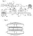
- Figure 1 schematically depicts a lithographic projection apparatus according to a particular embodiment of the invention.
- the apparatus comprises:
- the source LA (e. g. a laser-produced or discharge plasma source) produces a beam of radiation.
- This beam is fed into an illumination system (illuminator) IL, either directly or after having traversed conditioning means, such as a beam expander Ex, for example.
- the illuminator IL may comprise adjusting means AM for setting the outer and/or inner radial extent (commonly referred to as ⁇ -outer and ⁇ -inner, respectively) of the intensity distribution in the beam.
- ⁇ -outer and ⁇ -inner commonly referred to as ⁇ -outer and ⁇ -inner, respectively
- it will generally comprise various other components, such as an integrator IN and a condenser CO.
- the beam PB impinging on the mask MA has a desired uniformity and intensity distribution in its cross-section.
- the source LA may be within the housing of the lithographic projection apparatus (as is often the case when the source LA is a mercury lamp, for example), but that it may also be remote from the lithographic projection apparatus, the radiation beam which it produces being led into the apparatus (e.g. with the aid of suitable directing mirrors); this latter scenario is often the case when the source LA is an excimer laser.
- the current invention and Claims encompass both of these scenarios.
- the beam PB subsequently intercepts the mask MA, which is held on a mask table MT. Having been selectively reflected by the mask MA, the beam PB passes through the lens PL, which focuses the beam PB onto a target portion C of the substrate W. With the aid of the second positioning means (and interferometric measuring means IF), the substrate table WT can be moved accurately, e.g . so as to position different target portions C in the path of the beam PB. Similarly, the first positioning means can be used to accurately position the mask MA with respect to the path of the beam PB, e.g . after mechanical retrieval of the mask MA from a mask library, or during a scan.
- the mask table MT may just be connected to a short stroke actuator, or may be fixed.
- the depicted apparatus can be used in two different modes:
- Figure 2 depicts a side view of the magnetic assembly for a Lorentz actuator.
- the coil unit which consists of a coil 3 and cooling elements 1 is connected to the long stroke of the substrate or mask stage (WT or MT), while the magnets 4 with back irons 2 are connected to the short stroke of the mirror block, on which the substrate W or mask MA is mounted.
- changing magnetic fields linked by the conductive material of the cooling elements 1 cause eddy currents 5 to flow in the cooling elements 1.
- the sense of these eddy currents 5 is shown in Figure 3, for an increasing field directed into the page.
- the creation of eddy currents 5 provides a drag or damping force that opposes the actuator and reduces its performance.
- heat dissipated by the circulating currents reduces the effectiveness of the cooling element 1. This latter effect can be particularly damaging in EUV systems where a number of components are highly sensitive' to thermal expansion, which can be induced by radiation from warmer elements nearby.
- FIG. 4 The area 6 of the cooling plates 1 that is particularly prone to eddy currents, and in which it is most effective to locate means to control eddy currents 5, is indicated in Figure 4.
- Figure 5 illustrates how eddy currents 5 may be controlled according to the present invention by introducing slits 7 in the cooling element 1. Since the resistance across the slits 7 is extremely high, currents are forced to circulate around longer paths of smaller average cross-sectional area. Eddy currents 5 are therefore reduced due to the increased resistance of the eddy current paths. The dissipated heat varies as the square of the current and is therefore also reduced, as is the damping force.
- the arrangement in Figure 5 corresponds to a further preferred embodiment of the invention wherein the slits 7 are parallel to each other.
- This arrangement is beneficial because it favours a more uniform eddy current flow, so that induced temperature increases are spread out and reduced in magnitude.
- the slits are also arranged to be largely perpendicular to the eddy current flow depicted in Figure 3. This arrangement is desirable because it is particularly effective in increasing the resistance of eddy current paths.
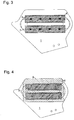
- Figures 6 and 7 depict an arrangement of slits 7 according to a further preferred embodiment of the present invention.
- the slits 7 are reduced in length in order to accommodate cooling channels in a more efficient manner.
- cooling channels 8 of reasonable cross-sectional area, therefore, it is necessary that they avoid the slits 7.
- An example arrangement for achieving this is depicted in Figure 7.
- the flow rate depends on the flow impedance of the cooling channel network.
- the flow impedance of the network depicted in Figure 7 is kept low by using short sections of cooling channel 8 connected together in parallel.
- the cooling channels 8 may have a substantially circular or a substantially rectangular cross-section.
Landscapes
- Physics & Mathematics (AREA)
- Engineering & Computer Science (AREA)
- Health & Medical Sciences (AREA)
- General Physics & Mathematics (AREA)
- Toxicology (AREA)
- Environmental & Geological Engineering (AREA)
- Life Sciences & Earth Sciences (AREA)
- Epidemiology (AREA)
- Atmospheric Sciences (AREA)
- Public Health (AREA)
- Chemical & Material Sciences (AREA)
- Combustion & Propulsion (AREA)
- Electromagnetism (AREA)
- Power Engineering (AREA)
- Exposure And Positioning Against Photoresist Photosensitive Materials (AREA)
- Linear Motors (AREA)
Abstract
Description
- a radiation system for supplying a projection beam of radiation;
- a support structure for supporting patterning means, the patterning means serving to pattern the projection beam according to a desired pattern;
- a substrate table for holding a substrate;
- a projection system for projecting the patterned beam onto a target portion of the substrate; and
- a Lorentz actuator, comprising a coil arrangement in thermal contact with at least one cooling element.
- A mask. The concept of a mask is well known in lithography, and it includes mask types such as binary, alternating phase-shift, and attenuated phase-shift, as well as various hybrid mask types. Placement of such a mask in the radiation beam causes selective transmission (in the case of a transmissive mask) or reflection (in the case of a reflective mask) of the radiation impinging on the mask, according to the pattern on the mask. In the case of a mask, the support structure will generally be a mask table, which ensures that the mask can be held at a desired position in the incoming radiation beam, and that it can be moved relative to the beam if so desired.
- A programmable mirror array. One example of such a device is a matrix-addressable surface having a viscoelastic control layer and a reflective surface. The basic principle behind such an apparatus is that (for example) addressed areas of the reflective surface reflect incident light as diffracted light, whereas unaddressed areas reflect incident light as undiffracted light. Using an appropriate filter, the said undiffracted light can be filtered out of the reflected beam, leaving only the diffracted light behind; in this manner, the beam becomes patterned according to the addressing pattern of the matrix-addressable surface. An alternative embodiment of a programmable mirror array employs a matrix arrangement of tiny mirrors, each of which can be individually tilted about an axis by applying a suitable localized electric field, or by employing piezoelectric actuation means. Once again, the mirrors are matrix-addressable, such that addressed mirrors will reflect an incoming radiation beam in a different direction to unaddressed mirrors; in this manner, the reflected beam is patterned according to the addressing pattern of the matrix-addressable mirrors. The required matrix addressing can be performed using suitable electronic means. In both of the situations described hereabove, the patterning means can comprise one or more programmable mirror arrays. More information on mirror arrays as here referred to can be gleaned, for example, from United States Patents US 5,296,891 and US 5,523,193, and PCT patent applications WO 98/38597 and WO 98/33096, which are incorporated herein by reference. In the case of a programmable mirror array, the said support structure may be embodied as a frame or table, for example, which may be fixed or movable as required.
- A programmable LCD array. An example of such a construction is given in United States Patent US 5,229,872, which is incorporated herein by reference. As above, the support structure in this case may be embodied as a frame or table, for example, which may be fixed or movable as required.
- providing a substrate that is at least partially covered by a layer of radiation-sensitive material;
- providing a projection beam of radiation using a radiation system;
- using patterning means to endow the projection beam with a pattern in its cross-section;
- projecting the patterned beam of radiation onto a target portion of the layer of radiation-sensitive material; and
- a Lorentz actuator, comprising a coil arrangement in thermal contact with at least one cooling element.
- a radiation system Ex, IL, for supplying a projection beam PB of radiation (e.g. EUV radiation), which in this particular case also comprises a radiation source LA;
- a first object table (mask table) MT provided with a mask holder for holding a mask MA (e.g. a reticle), and connected to first positioning means for accurately positioning the mask with respect to item PL;
- a second object table (substrate table) WT provided with a substrate holder for holding a substrate W (e.g. a resist-coated silicon wafer), and connected to second positioning means for accurately positioning the substrate with respect to item PL;
- a projection system ("lens") PL (e.g. a mirror group) for imaging an irradiated portion of the mask MA onto a target portion C (e.g. comprising one or more dies) of the substrate W.
Claims (10)
- A lithographic projection apparatus comprising:characterized in that one or more slits are provided in said cooling element, arranged so as to increase the electrical resistance of eddy current paths.a radiation system for providing a projection beam of radiation;a support structure for supporting patterning means, the patterning means serving to pattern the projection beam according to a desired pattern;a substrate table for holding a substrate;a projection system for projecting the patterned beam onto a target portion of the substrate; anda Lorentz actuator, comprising a coil arrangement in thermal contact with at least one cooling element,
- A lithographic projection apparatus according to claim 1, wherein the slits are arranged to be substantially parallel to each other.
- A lithographic projection apparatus according to any one of the preceding claims, wherein the slits are arranged to be substantially perpendicular to the direction of the induced electric field.
- A lithographic projection apparatus according to any one of the preceding claims, wherein the slits are arranged to be substantially parallel, or at a substantially oblique angle, to the direction of the induced electric field.
- A lithographic projection apparatus according to any one of the preceding claims wherein the slit lengths are limited so as not to extend across the entire length of the cooling element.
- A lithographic projection apparatus according to any one of the preceding claims wherein adjacent slits extend from opposite sides of the cooling element.
- A lithographic projection apparatus according to any one of the preceding claims wherein cooling channels are integrated with the slits in such a way as to provide a plurality of parallel paths arranged to reduce flow impedance.
- A lithographic projection apparatus according to any of the preceding claims wherein cooling channels are arranged in a substantially symmetrical network to provide uniform coverage of the cooling element.
- A lithographic projection apparatus according to any one of the preceding claims wherein the slits are filled to protect from outgassing from the coil.
- A device manufacturing method comprising the steps of:characterized in that one or more slits are provided in said cooling element, arranged so as to increase the electrical resistance of eddy current paths.providing a substrate that is at least partially covered by a layer of radiation-sensitive material;providing a projection beam of radiation using a radiation system;using patterning means to endow the projection beam with a pattern in its cross-section;projecting the patterned beam of radiation onto a target portion of the layer of radiation-sensitive material; andoperating a Lorentz actuator, which comprises a coil arrangement in thermal contact with at least one cooling element
Priority Applications (1)
| Application Number | Priority Date | Filing Date | Title |
|---|---|---|---|
| EP04251284A EP1465014B1 (en) | 2003-03-11 | 2004-03-05 | Lithographic apparatus, device manufacturing method and device manufacturated thereby |
Applications Claiming Priority (3)
| Application Number | Priority Date | Filing Date | Title |
|---|---|---|---|
| EP03251446A EP1457825A1 (en) | 2003-03-11 | 2003-03-11 | Lithographic apparatus, device manufacturing method and device manufactured thereby |
| EP03251446 | 2003-03-11 | ||
| EP04251284A EP1465014B1 (en) | 2003-03-11 | 2004-03-05 | Lithographic apparatus, device manufacturing method and device manufacturated thereby |
Publications (3)
| Publication Number | Publication Date |
|---|---|
| EP1465014A2 true EP1465014A2 (en) | 2004-10-06 |
| EP1465014A3 EP1465014A3 (en) | 2006-08-09 |
| EP1465014B1 EP1465014B1 (en) | 2008-08-06 |
Family
ID=32852248
Family Applications (1)
| Application Number | Title | Priority Date | Filing Date |
|---|---|---|---|
| EP04251284A Expired - Lifetime EP1465014B1 (en) | 2003-03-11 | 2004-03-05 | Lithographic apparatus, device manufacturing method and device manufacturated thereby |
Country Status (1)
| Country | Link |
|---|---|
| EP (1) | EP1465014B1 (en) |
Cited By (1)
| Publication number | Priority date | Publication date | Assignee | Title |
|---|---|---|---|---|
| CN109477902A (en) * | 2016-01-29 | 2019-03-15 | 上海联影医疗科技有限公司 | Method and apparatus for temperature control in a PET detector |
Family Cites Families (3)
| Publication number | Priority date | Publication date | Assignee | Title |
|---|---|---|---|---|
| TW385456B (en) * | 1997-05-08 | 2000-03-21 | Sumitomo Electric Industries | Superconduction coil |
| US6476383B1 (en) * | 1999-08-31 | 2002-11-05 | Max-Planck-Gesellschaft Zur Forderung Der Wissenschaften E.V. | Device and method for generating and manipulating coherent matter waves |
| JP4257118B2 (en) * | 2001-01-25 | 2009-04-22 | コーニンクレッカ フィリップス エレクトロニクス エヌ ヴィ | Coil with cooling means |
-
2004
- 2004-03-05 EP EP04251284A patent/EP1465014B1/en not_active Expired - Lifetime
Cited By (1)
| Publication number | Priority date | Publication date | Assignee | Title |
|---|---|---|---|---|
| CN109477902A (en) * | 2016-01-29 | 2019-03-15 | 上海联影医疗科技有限公司 | Method and apparatus for temperature control in a PET detector |
Also Published As
| Publication number | Publication date |
|---|---|
| EP1465014A3 (en) | 2006-08-09 |
| EP1465014B1 (en) | 2008-08-06 |
Similar Documents
| Publication | Publication Date | Title |
|---|---|---|
| US6717296B2 (en) | Lithographic apparatus and motor for use in the apparatus | |
| US7126666B2 (en) | Lithographic apparatus, device manufacturing method and device manufactured thereby | |
| US7081943B2 (en) | Lithographic apparatus and device manufacturing method | |
| EP1477855B1 (en) | Lithographic apparatus and device manufacturing method | |
| US6891600B2 (en) | Lithographic apparatus and device manufacturing method | |
| EP1519230A1 (en) | Lithographic apparatus and device manufacturing method | |
| US7088428B2 (en) | Lithographic actuator mechanism, lithographic apparatus, and device manufacturing method | |
| US20010013580A1 (en) | Cooling of voice coil motors in lithographic projection apparatus | |
| US6630984B2 (en) | Lithographic apparatus, device manufacturing method, and device manufactured thereby | |
| US7167234B2 (en) | Actuator assembly and lithographic apparatus comprising such an actuator assembly | |
| EP1457826A1 (en) | Lithographic apparatus and device manufacturing method | |
| US7079226B2 (en) | Lithographic actuator mechanism, lithographic apparatus, and device manufacturing method | |
| EP1124160A2 (en) | Cooling of oscillating linear motors in lithographic projection apparatus | |
| EP1178357A1 (en) | Lithographic apparatus | |
| EP1465014B1 (en) | Lithographic apparatus, device manufacturing method and device manufacturated thereby | |
| EP1286222A1 (en) | Lithographic apparatus and device manufacturing method | |
| EP1457833B1 (en) | Lithographic apparatus, device manufacturing method, and device manufactured thereby | |
| EP1475669A1 (en) | Lithographic apparatus, device manufacturing method, and device manufactured thereby | |
| EP1243970A1 (en) | Lithographic apparatus |
Legal Events
| Date | Code | Title | Description |
|---|---|---|---|
| PUAI | Public reference made under article 153(3) epc to a published international application that has entered the european phase |
Free format text: ORIGINAL CODE: 0009012 |
|
| AK | Designated contracting states |
Kind code of ref document: A2 Designated state(s): AT BE BG CH CY CZ DE DK EE ES FI FR GB GR HU IE IT LI LU MC NL PL PT RO SE SI SK TR |
|
| AX | Request for extension of the european patent |
Extension state: AL HR LT LV MK |
|
| PUAL | Search report despatched |
Free format text: ORIGINAL CODE: 0009013 |
|
| AK | Designated contracting states |
Kind code of ref document: A3 Designated state(s): AT BE BG CH CY CZ DE DK EE ES FI FR GB GR HU IE IT LI LU MC NL PL PT RO SE SI SK TR |
|
| AX | Request for extension of the european patent |
Extension state: AL LT LV MK |
|
| RIC1 | Information provided on ipc code assigned before grant |
Ipc: G03F 7/20 20060101AFI20040525BHEP Ipc: H02K 41/00 20060101ALI20060706BHEP Ipc: H02K 41/02 20060101ALI20060706BHEP |
|
| 17P | Request for examination filed |
Effective date: 20070125 |
|
| AKX | Designation fees paid |
Designated state(s): DE FR GB IT NL |
|
| GRAP | Despatch of communication of intention to grant a patent |
Free format text: ORIGINAL CODE: EPIDOSNIGR1 |
|
| RIN1 | Information on inventor provided before grant (corrected) |
Inventor name: VREUGDEWATER, PATRICIA Inventor name: VAN DER SCHOOT, HARMEN KLAAS Inventor name: HOL, SVEN ANTOIN JOHAN Inventor name: BUIJS, EDWIN JOHAN |
|
| GRAS | Grant fee paid |
Free format text: ORIGINAL CODE: EPIDOSNIGR3 |
|
| GRAA | (expected) grant |
Free format text: ORIGINAL CODE: 0009210 |
|
| AK | Designated contracting states |
Kind code of ref document: B1 Designated state(s): DE FR GB IT NL |
|
| REG | Reference to a national code |
Ref country code: GB Ref legal event code: FG4D |
|
| REF | Corresponds to: |
Ref document number: 602004015523 Country of ref document: DE Date of ref document: 20080918 Kind code of ref document: P |
|
| PLBE | No opposition filed within time limit |
Free format text: ORIGINAL CODE: 0009261 |
|
| STAA | Information on the status of an ep patent application or granted ep patent |
Free format text: STATUS: NO OPPOSITION FILED WITHIN TIME LIMIT |
|
| 26N | No opposition filed |
Effective date: 20090507 |
|
| REG | Reference to a national code |
Ref country code: FR Ref legal event code: PLFP Year of fee payment: 13 |
|
| REG | Reference to a national code |
Ref country code: FR Ref legal event code: PLFP Year of fee payment: 14 |
|
| REG | Reference to a national code |
Ref country code: FR Ref legal event code: PLFP Year of fee payment: 15 |
|
| PGFP | Annual fee paid to national office [announced via postgrant information from national office to epo] |
Ref country code: GB Payment date: 20220322 Year of fee payment: 19 |
|
| PGFP | Annual fee paid to national office [announced via postgrant information from national office to epo] |
Ref country code: IT Payment date: 20220323 Year of fee payment: 19 |
|
| PGFP | Annual fee paid to national office [announced via postgrant information from national office to epo] |
Ref country code: FR Payment date: 20230323 Year of fee payment: 20 |
|
| PGFP | Annual fee paid to national office [announced via postgrant information from national office to epo] |
Ref country code: DE Payment date: 20230328 Year of fee payment: 20 |
|
| P01 | Opt-out of the competence of the unified patent court (upc) registered |
Effective date: 20230403 |
|
| PGFP | Annual fee paid to national office [announced via postgrant information from national office to epo] |
Ref country code: NL Payment date: 20230323 Year of fee payment: 20 |
|
| GBPC | Gb: european patent ceased through non-payment of renewal fee |
Effective date: 20230305 |
|
| PG25 | Lapsed in a contracting state [announced via postgrant information from national office to epo] |
Ref country code: GB Free format text: LAPSE BECAUSE OF NON-PAYMENT OF DUE FEES Effective date: 20230305 |
|
| PG25 | Lapsed in a contracting state [announced via postgrant information from national office to epo] |
Ref country code: GB Free format text: LAPSE BECAUSE OF NON-PAYMENT OF DUE FEES Effective date: 20230305 |
|
| REG | Reference to a national code |
Ref country code: DE Ref legal event code: R071 Ref document number: 602004015523 Country of ref document: DE |
|
| REG | Reference to a national code |
Ref country code: NL Ref legal event code: MK Effective date: 20240304 |
|
| PG25 | Lapsed in a contracting state [announced via postgrant information from national office to epo] |
Ref country code: IT Free format text: LAPSE BECAUSE OF NON-PAYMENT OF DUE FEES Effective date: 20230305 |