EP1463292A2 - Image exposing apparatus - Google Patents
Image exposing apparatus Download PDFInfo
- Publication number
- EP1463292A2 EP1463292A2 EP04007118A EP04007118A EP1463292A2 EP 1463292 A2 EP1463292 A2 EP 1463292A2 EP 04007118 A EP04007118 A EP 04007118A EP 04007118 A EP04007118 A EP 04007118A EP 1463292 A2 EP1463292 A2 EP 1463292A2
- Authority
- EP
- European Patent Office
- Prior art keywords
- light source
- array
- light
- rows
- array light
- Prior art date
- Legal status (The legal status is an assumption and is not a legal conclusion. Google has not performed a legal analysis and makes no representation as to the accuracy of the status listed.)
- Withdrawn
Links
- 239000000463 material Substances 0.000 claims abstract description 26
- 229910052709 silver Inorganic materials 0.000 claims abstract description 21
- 239000004332 silver Substances 0.000 claims abstract description 21
- -1 silver halide Chemical class 0.000 claims abstract description 21
- 238000002474 experimental method Methods 0.000 description 34
- 238000011156 evaluation Methods 0.000 description 26
- 238000000034 method Methods 0.000 description 19
- 230000000007 visual effect Effects 0.000 description 17
- 230000007423 decrease Effects 0.000 description 14
- 239000006185 dispersion Substances 0.000 description 13
- 239000007787 solid Substances 0.000 description 12
- 238000003491 array Methods 0.000 description 9
- 238000004519 manufacturing process Methods 0.000 description 9
- 230000004907 flux Effects 0.000 description 6
- 238000005259 measurement Methods 0.000 description 4
- 230000007246 mechanism Effects 0.000 description 4
- 230000002265 prevention Effects 0.000 description 3
- 238000013461 design Methods 0.000 description 2
- 238000010586 diagram Methods 0.000 description 2
- 238000009826 distribution Methods 0.000 description 2
- 230000005540 biological transmission Effects 0.000 description 1
- 239000003086 colorant Substances 0.000 description 1
- 238000004040 coloring Methods 0.000 description 1
- 230000000694 effects Effects 0.000 description 1
- 239000013307 optical fiber Substances 0.000 description 1
- 230000008569 process Effects 0.000 description 1
- 238000012545 processing Methods 0.000 description 1
- 238000000926 separation method Methods 0.000 description 1
Images

Classifications
-
- H—ELECTRICITY
- H04—ELECTRIC COMMUNICATION TECHNIQUE
- H04N—PICTORIAL COMMUNICATION, e.g. TELEVISION
- H04N1/00—Scanning, transmission or reproduction of documents or the like, e.g. facsimile transmission; Details thereof
- H04N1/04—Scanning arrangements, i.e. arrangements for the displacement of active reading or reproducing elements relative to the original or reproducing medium, or vice versa
- H04N1/19—Scanning arrangements, i.e. arrangements for the displacement of active reading or reproducing elements relative to the original or reproducing medium, or vice versa using multi-element arrays
- H04N1/191—Scanning arrangements, i.e. arrangements for the displacement of active reading or reproducing elements relative to the original or reproducing medium, or vice versa using multi-element arrays the array comprising a one-dimensional array, or a combination of one-dimensional arrays, or a substantially one-dimensional array, e.g. an array of staggered elements
- H04N1/192—Simultaneously or substantially simultaneously scanning picture elements on one main scanning line
- H04N1/193—Simultaneously or substantially simultaneously scanning picture elements on one main scanning line using electrically scanned linear arrays, e.g. linear CCD arrays
- H04N1/1932—Simultaneously or substantially simultaneously scanning picture elements on one main scanning line using electrically scanned linear arrays, e.g. linear CCD arrays using an array of elements displaced from one another in the sub scan direction, e.g. a diagonally arranged array
- H04N1/1933—Staggered element arrays, e.g. arrays with elements arranged in a zigzag
-
- B—PERFORMING OPERATIONS; TRANSPORTING
- B41—PRINTING; LINING MACHINES; TYPEWRITERS; STAMPS
- B41J—TYPEWRITERS; SELECTIVE PRINTING MECHANISMS, i.e. MECHANISMS PRINTING OTHERWISE THAN FROM A FORME; CORRECTION OF TYPOGRAPHICAL ERRORS
- B41J2/00—Typewriters or selective printing mechanisms characterised by the printing or marking process for which they are designed
- B41J2/435—Typewriters or selective printing mechanisms characterised by the printing or marking process for which they are designed characterised by selective application of radiation to a printing material or impression-transfer material
- B41J2/447—Typewriters or selective printing mechanisms characterised by the printing or marking process for which they are designed characterised by selective application of radiation to a printing material or impression-transfer material using arrays of radiation sources
- B41J2/45—Typewriters or selective printing mechanisms characterised by the printing or marking process for which they are designed characterised by selective application of radiation to a printing material or impression-transfer material using arrays of radiation sources using light-emitting diode [LED] or laser arrays
- B41J2/451—Special optical means therefor, e.g. lenses, mirrors, focusing means
-
- H—ELECTRICITY
- H04—ELECTRIC COMMUNICATION TECHNIQUE
- H04N—PICTORIAL COMMUNICATION, e.g. TELEVISION
- H04N1/00—Scanning, transmission or reproduction of documents or the like, e.g. facsimile transmission; Details thereof
- H04N1/04—Scanning arrangements, i.e. arrangements for the displacement of active reading or reproducing elements relative to the original or reproducing medium, or vice versa
- H04N1/19—Scanning arrangements, i.e. arrangements for the displacement of active reading or reproducing elements relative to the original or reproducing medium, or vice versa using multi-element arrays
- H04N1/191—Scanning arrangements, i.e. arrangements for the displacement of active reading or reproducing elements relative to the original or reproducing medium, or vice versa using multi-element arrays the array comprising a one-dimensional array, or a combination of one-dimensional arrays, or a substantially one-dimensional array, e.g. an array of staggered elements
- H04N1/192—Simultaneously or substantially simultaneously scanning picture elements on one main scanning line
- H04N1/193—Simultaneously or substantially simultaneously scanning picture elements on one main scanning line using electrically scanned linear arrays, e.g. linear CCD arrays
Definitions
- the present invention relates to an image exposing apparatus, and in particular, to an image exposing apparatus wherein a silver halide photosensitive material is exposed to light image which is emitted from each of plural array light sources and has a different wavelength.
- an image exposing apparatus wherein an array light source having plural light emitting devices is provided for each recording color, and a silver halide photosensitive material such as a printing paper is exposed to light image, and the image exposing apparatus has been put to practical use.
- an image exposing apparatus wherein light emitted from an array light source for each recording color is mixed to form a line-shaped light flux, and this line-shaped light flux is converged on a photosensitive material by a light-converging means so that exposure is made (for example, see Patent Document 1).
- the light-converging means there is used a selfoc lens array representing a line-shaped same-size erect image forming lens that is composed of plural selfoc lenses arranged in a single row or in plural rows.
- a size of a light emitting device of the array light source For establishing a pixel size to an appropriate value with a purpose of preventing the decline of image quality, it is necessary to establish a size of a light emitting device of the array light source to be an appropriate value.
- a light emitting device size of the array light source the size that is close to a distance between centers of light emitting devices, which are brought into a line, is preferable.
- electric wiring that controls individual light emitting device is needed, and a precise and specific structure is required, which results in difficult manufacturing and worse yield.
- plural light emitting devices are arranged to be in plural rows, and one of the adjoining rows is shifted in the longitudinal direction to be in a zigzag form, and thereby, the various problems stated above are solved, and a size of the light emitting device is established easily, thus, a decline of image quality is prevented.
- a distance from an array light source to a light-converging means it is preferable to make a distance from an array light source to a light-converging means to be as short as possible because light that is emitted from the array light source is diffused. Therefore, arrangement of parts is extremely restricted, including necessity to house a light-mixing member in a small space between the array light source and the light-converging means, and the light-mixing member is required to have compactness and a precise and specific structure. Further, because of the aforementioned restriction on parts arrangement, the array light source is also required to have a specific structure (for example, a structure of a thin type employing a high-strength specific material). Further, in the case of incorporating parts, precision operations wherein a tolerance is small are needed, which results in an increase of manufacturing cost.
- a lens having a large aperture for example, selfoc lens arrays in many rows
- a lens having a large aperture is employed as a light-converging means, in recent years. Namely, when, a lens having a large aperture is used, it is possible to make a distance from the array light source to the lens to be relatively long, thereby, the restriction on parts arrangement is eased, and an increase of manufacturing cost can be controlled consequently.
- dispersion in exposure positions is caused by a difference of characteristic of each lens.
- dispersion in exposure positions tends to be caused by a difference of characteristic of each selfoc lens element and by an assembly error of an array. It is of common knowledge that the longer the selfoc lens is, the easier the dispersion of image forming positions is caused.
- an exposure line in one row is formed by combining exposure points of respective light emitting device rows, and therefore, "streaks" are easily formed on an image if dispersion of the exposure positions is caused.
- the density of these "streaks” is about a half that of writing by the array light source, and further, the “streaks” are emphasized by peculiar characteristics of a silver halide photosensitive material, thus, the streaks are recognized by human eyes, resulting in a decline of image quality.
- An objects of the invention is to prevent a decline of image quality by stopping actualization of "streaks" which are formed by dispersion of exposure positions which have origin in using an array light source having plural light emitting device rows and a lens having a large aperture, and by characteristics of a silver halide photosensitive material.
- An image exposing apparatus having therein an array light source wherein there are arranged a plurality of rows of light emitting devices in which a plurality of light emitting devices are arranged in a form of a line, and the adjoining light emitting device rows is shifted in the longitudinal direction to form a zigzag form, and a light-converging means that converges emitted light on a silver halide photosensitive material, wherein an interval of the light emitting device rows of array light sources in a zigzag form is established to be within 500 ⁇ m.
- An image exposing apparatus having therein an array light source group wherein there are arranged a plurality of rows of light emitting devices in which a plurality of light emitting devices are arranged in a form of a line, and one of the adjoining light emitting device rows is shifted in the longitudinal direction to form a zigzag form, a light-mixing means (device) that mixes light emitted from the array light source group and forms emitted light in a line form, and a light-converging means (device) that converges emitted light formed by the light mixing means (device) on a silver halide photosensitive material, wherein an interval of the light emitting device rows of array light sources in a zigzag form is established to be within 500 ⁇ m.
- the image exposing apparatus according to the Structure (1) or (2), wherein the light-converging means (device) is a selfoc lens array in which a plurality of rows of selfoc lens devices (elements) are arranged.
- the image exposing apparatus according to any one of the Structures (1) to (3), wherein writing density of the array light source is established to be 210 dpi or more.
- writing density for the array light source group is established to be 210 dpi or more. Namely, when the writing density for the array light source group is lower than 210 dpi, scanning lines becomes conspicuous, and thereby, image quality is lowered even when "streaks" are not formed. However, it is possible to make the scanning lines not to be conspicuous by establishing writing density for the array light source group to be 210 dpi or more. Therefore, a decline of image quality can be prevented.
- the image exposing apparatus according to any one of the Structures (1) to (4), wherein writing density of the array light source is established to be 440 dpi or less.
- streaks are conspicuous when the writing density is 440 dpi or less.
- the limitations of any of the Structures 1 - 4 it is possible to make the streaks not to be conspicuous.
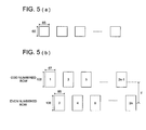
- FIG. 5 (a) and Fig. 5 (b) is an illustration for illustrating arrangement of light emitting devices of the array light source of the image exposing apparatus relating to the second embodiment of the invention.
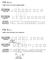
- FIG. 6 (a) and Fig. 6 (b) is an illustration for illustrating a process of forming "streaks" which are formed when a conventional image exposing apparatus is used.
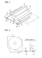
- Fig. 1 is a schematic perspective view showing the structure in the vicinity of the array light source of an image exposing apparatus relating to the present embodiment
- Fig. 2 is a schematic side view showing the overall structure (excluding the structure in the vicinity of the array light source) of the image exposing apparatus shown in Fig. 1.
- Fig. 3 is an illustration for illustrating arrangement of light emitting devices of the array light source of the image exposing apparatus shown in Fig. 1.
- Fig. 4 is a block diagram showing an electric structure of the image exposing apparatus shown in Fig. 1.
- the image exposing apparatus relating to the present embodiment is provided with paper magazine 11 on which printing paper 10 representing a silver halide photosensitive material is wound in a roll shape to be held, driving rollers 12a, 12b, 12c and 12d which convey the printing paper 10 at a prescribed conveyance speed and cutter 13 that cuts exposed printing paper 10 into a prescribed size.
- the image exposing apparatus relating to the present embodiment is provided with first array light source 21 composed of light emitting devices in an array form conducting exposure with the first light (red), second array light source 22 composed of light emitting devices in an array form conducting exposure with the second light (green) and third array light source 23 composed of light emitting devices in an array form conducting exposure with the third light (blue).
- first array light source 21 - third array light source 23 represent an array light source group in the invention.
- the first array light source 21 is composed of a vacuum fluorescent print head (Vacuum Fluorescent Print Head: hereinafter referred to as "VFPH") representing light emitting devices arranged in an array form and of a red filter that converts light emitted from VFPH into red light.
- VFPH vacuum fluorescent print head
- the first array light source 21 has a zigzag arrangement wherein two rows of light emitting devices composed of arranged light emitting devices each being in size of 85 ⁇ m x 85 ⁇ m are arranged at prescribed interval of d. Namely, when numbers are given to light emitting devices as shown in Fig.
- odd-numbered rows each being composed of a group of light emitting devices each having an odd number are arranged to be staggered in the longitudinal direction for even-numbered rows each being composed of a group of light emitting devices each having an even number.
- a distance between adjoining centers of light emitting devices in each row of odd-numbered rows and even-numbered rows is set to 85 ⁇ m.
- second array light source 22 is composed of VFPH and green filters
- third array light source 23 is composed of VFPH and blue filters.
- Each of these second array light source 22 and third array light source 23 has a zigzag arrangement wherein two rows of light emitting devices composed of arranged light emitting devices each being in size of 85 ⁇ m x 85 ⁇ m are arranged at prescribed interval of d, in the same way as in the first array light source 21.
- the image exposing apparatus relating to the present embodiment is provided with dichroic prism (light-mixing means) 30 that mixes a light flux emitted from an array light source for each recording color, and makes respective light fluxes each having a different color to emerge through the same path.
- the dichroic prism 30 is provided with first transparent member 31 which is in a shape of a long triangular prism, second transparent member 32 which is in a shape of a long pentagonal prism and third transparent member 33 which is in a shape of a long quadratic prism, and longer side surfaces of respective transparent members are cemented each other.
- first light selection film On a cementing surface between the first transparent member 31 and the second transparent member 32 of the dichroic prism 30 and on a cementing surface between the second transparent member 32 and the third transparent member 33, there are provided respectively a first light selection film and a second light selection film (not shown) each transmits light or reflects light selectively in accordance with each wavelength.
- the first light selection film is one which transmits first light (red) and reflects third light (blue), while, the second light selection film functions to transmit the first light (red) and the third light (blue) and to reflect the second light (green).
- the image exposing apparatus relating to the present embodiment is provided with selfoc lens array (light-converging means) 40 that converges a light flux with each recording color mixed by the dichroic prism 30 on a photosensitive material for making exposure.
- selfoc lens array 40 in four rows or six rows is used.
- the image exposing apparatus relating to the present embodiment is provided with CPU 50 serving as a control means that controls each portion, head driver control circuit (HDC circuit) 60 that receives image data from the outside and generates image signals for driving an array light source for each color, head driver circuit (HD circuit) 71 that receives image signals of first light (red) coming from HDC circuit 31 and generates light-emitting signals for making a light emitting device of the first array light source 21 in accordance with gradation, head driver circuit (HD circuit) 72 that receives image signals of second light (green) coming from HDC circuit 32 and generates light-emitting signals for making a light emitting device of the second array light source 22 in accordance with gradation, head driver circuit (HD circuit) 73 that receives image signals of third light (blue) coming from HDC circuit 33 and generates light-emitting signals for making a light emitting device of the third array light source 23 in accordance with gradation, and printing paper conveyance mechanism 80 that is composed of a driving
- CPU 50 feeds out printing paper 10 at prescribed speed by means of the printing paper conveyance mechanism 80. Then, color image data coming from cameras and image processing circuits in the outside are separated to each color image signal in HDC circuit 60.
- HD circuits 71 - 73 which have received image signals in respective colors from HDC circuit 60 at the same timing generate light-emitting signals that make light emitting devices of array light sources to emit light in accordance with gradation of the image signals.
- First array light source 21 - third array light source 23 which have received the light-emitting signals from HD circuits 71 - 73 emit light in accordance with image signals for each color at the same timing.
- first array light source 21 - third array light source 23 an exposure line in one row is formed by combining exposure points of respective light emitting device rows, and therefore, "streaks" are easily formed on an image if dispersion of the exposure positions is caused, which has been mentioned earlier.
- the "streaks" of this kind are emphasized especially in the case of using a silver halide photosensitive material (printing paper 10), and the reasons for the foregoing are guessed as follows.
- exposure energy is expressed by the product of luminance of a light source and exposure time
- a silver halide photosensitive material has complicated characteristics (relationship between exposure energy and density) that color forming characteristic on the occasion where exposures for the same color are conducted twice intermittently is different from that on the occasion where exposure is conducted once, independent of the total exposure energy that is the same for the both occasions.
- the silver halide photosensitive material since a silver halide photosensitive material is constructed by forming plural layers on a base paper called a support, the silver halide photosensitive material has a characteristic that light used for exposure is diffused by reflection and scattering between layers and inside the layer and by reflection and scattering on the base paper, and thereby, formed images are spread.
- images for measurement thus formed are measured by a reflection densitometer of a scanning type and positional relationship between exposure positions of odd-numbered rows and exposure positions of even-numbered rows is obtained to calculates the maximum value of a difference from a design value (amount of deviation of pixel ⁇ : see Fig. 6 (b)).
- the calculation of this kind for amount of deviation of pixel ⁇ was conducted for each of fifty selfoc lens arrays 40 (in 4 rows) to obtain a distribution, and a value obtained by adding doubled standard deviation to a mean value was made to be an evaluation value (evaluation of an amount of deviation of a pixel).
- gray solid images having uniform density of 0.8 are formed. Then, after observing the gray solid images thus formed, there was conducted evaluation wherein "NG” represented an occasion where "streaks” were observed and “G” represented an occasion where "streaks” were not observed (visual evaluation).
- gray solid images having density of 0.8 for each writing density D are formed by using selfoc lens arrays 40 in four rows. After that, the gray solid images thus formed are observed to conduct evaluation wherein "NG” represents an occasion where scanning lines are observed in images and "G” represents an occasion where no scanning lines are observed (visual evaluation).
- the third array light source 23 when writing density D of the first array light source 21 - the third array light source 23 is not more than 440 dpi, in particular, it is necessary to prevent forming of "streaks" by establishing interval between light emitting device rows "d" to be 500 ⁇ m or less.
- first array light source 21 - third array light source 23 Since the interval between light emitting device rows "d" of the array light source in a zigzag arrangement (first array light source 21 - third array light source 23) is established to be within 500 ⁇ m, in the image exposing apparatus relating to the embodiment explained above, it is possible to prevent actualization of "streaks" formed by a cause of dispersion of exposure positions by light emitted from the array light source group, which results in prevention of a decline of image quality.
- the image exposing apparatus relating to the present embodiment, it is possible to make a distance from the array light source group (first array light source 21 - third array light source 23) to selfoc lens array 40 to be relatively long, and thereby to ease restriction for parts arrangement. As a result, an increase of manufacturing cost can be controlled.
- writing density of the array light source group (first array light source 21 - third array light source 23) is established to be 210 dpi or more (300 dpi). Namely, when writing density of the array light source group (first array light source 21 - third array light source 23) is lower than 210 dpi, image quality is lowered even when no "streaks" are formed because scanning lines become conspicuous. However, it is possible to make scanning lines not to be conspicuous by setting writing density of the array light source group (first array light source 21 - third array light source 23) to be 210 dpi or more, and thereby to prevent a decline of image quality.
- the image exposing apparatus relating to the present embodiment is one wherein the structure of the array light source of the image exposing apparatus relating to the first embodiment is modified, and other structures are substantially the same. Therefore, explanation for the overlapped structures will be omitted.
- Fig. 5 is an illustration for illustrating a light emitting device arrangement of the array light source of the image exposing apparatus relating to the present embodiment.
- the first array light source composed of an array-shaped light emitting device that makes exposure for the first light (red) comprises light emitting devices in a single row which are made up of arranged LEDs each having a size of 65 ⁇ m x 65 ⁇ m, as is shown in Fig. 5 (a).
- a distance between centers of light emitting devices in a row is set to 85 ⁇ m.
- the second array light source is composed of VFPH and a green filter
- the third array light source 23 is composed of VFPH and a blue filter.
- each of these second array light source 22 and third array light source 23 has a zigzag arrangement wherein two rows of arranged light emitting devices each having a size of 67 ⁇ m x 108 ⁇ m are placed in order at a prescribed interval d.
- a distance between adjoining centers of light emitting devices in each row of odd-numbered rows and even-numbered rows is set to 85 ⁇ m.
- interval between light emitting device rows "d” is established to be different each other. Further, interval between light emitting device rows “d” in the array light source group was set to be about 1000 ⁇ m, so that "streaks" may be formed intentionally. Then, for each interval between light emitting device rows "d", images for measurement are formed in the situation where the rows are divided into odd-numbered rows and even-numbered rows.
- images for measurement thus formed are measured by a reflection densitometer of a scanning type and positional relationship between exposure positions of odd-numbered rows and exposure positions of even-numbered rows is obtained to calculates the maximum value of a difference from a design value (amount of deviation of pixel ⁇ : see Fig. 6 (b)).
- the calculation of this kind for amount of deviation of pixel ⁇ was conducted for each of fifty selfoc lens arrays 40 (in 4 rows) to obtain a distribution, and a value obtained by adding doubled standard deviation to a mean value was made to be an evaluation value (evaluation of an amount of deviation of a pixel).
- gray solid images having uniform density of 0.8 are formed for each. Then, after observing the gray solid images thus formed, there was conducted evaluation wherein "NG” represented an occasion where "streaks” were observed and “G” represented an occasion where "streaks” were not observed (visual evaluation).
- the interval between light emitting device rows "d" for the array light source in a zigzag arrangement is established to be within 500 ⁇ m, and therefore, it is possible to prevent actualization of "streaks" which are formed by a cause of dispersion of exposure positions of light emitted from the array light source group, which results in prevention of a decline of image quality.
- a dichroic prism is employed as a light mixing means in the aforementioned embodiment, it is also possible to employ a dichroic mirror and an aggregate of optical fibers that mixes light fluxes entering plural ends of incidence and transmits them to one end of emergence, as a light mixing means.
- an interval between light emitting device rows of the array light source in a zigzag arrangement is established to be within a specific range (within 500 ⁇ m), thus, it is possible to prevent actualization of "streaks" which are formed by a cause of dispersion of exposure positions of light emitted from the array light source group. As a result, a decline of image quality can be prevented.
Landscapes
- Engineering & Computer Science (AREA)
- Multimedia (AREA)
- Signal Processing (AREA)
- Physics & Mathematics (AREA)
- Optics & Photonics (AREA)
- Health & Medical Sciences (AREA)
- General Health & Medical Sciences (AREA)
- Toxicology (AREA)
- Printers Or Recording Devices Using Electromagnetic And Radiation Means (AREA)
- Facsimile Heads (AREA)
Abstract
An image exposing apparatus for exposing an image on a
silver halide photosensitive material, including an array
light source for emitting a light image, the array light
source having a plurality of rows of light emitting devices,
each of the plurality of rows having a plurality of light
emitting devices arranged in a form of a line, and one of
adjoining two rows of the plurality of rows of light emitting
devices being shifted in the longitudinal direction to form a
zigzag arrangement of light emitting devices; and a light
converging device for converging the light image emitted from
the array light sources onto a silver halide photosensitive
material, wherein an interval between each of the plurality
of rows of light emitting device is not larger than 500 µm.
Description
The present invention relates to an image exposing
apparatus, and in particular, to an image exposing apparatus
wherein a silver halide photosensitive material is exposed to
light image which is emitted from each of plural array light
sources and has a different wavelength.
Heretofore, there has been proposed an image exposing
apparatus wherein an array light source having plural light
emitting devices is provided for each recording color, and a
silver halide photosensitive material such as a printing
paper is exposed to light image, and the image exposing
apparatus has been put to practical use. In recent years,
there has been proposed an image exposing apparatus wherein
light emitted from an array light source for each recording
color is mixed to form a line-shaped light flux, and this
line-shaped light flux is converged on a photosensitive
material by a light-converging means so that exposure is made
(for example, see Patent Document 1). As the light-converging
means, there is used a selfoc lens array
representing a line-shaped same-size erect image forming lens
that is composed of plural selfoc lenses arranged in a single
row or in plural rows.
When making exposure by using the image exposing
apparatus of this kind, it is necessary to establish a size
(pixel size) of a pixel formed on a photosensitive material
by exposure to an appropriate value. The reason for this is
that when a pixel size is too small to cause a large gap
between pixels, it sometimes becomes difficult to obtain high
density, resulting in an image that lacks crispness, and when
a pixel size is too large to cause considerable overlapping
of pixels, on the other hand, line image sometimes becomes
thick or an image lacks sharpness, resulting in a decline of
image quality.
For establishing a pixel size to an appropriate value
with a purpose of preventing the decline of image quality, it
is necessary to establish a size of a light emitting device
of the array light source to be an appropriate value. As a
light emitting device size of the array light source, the
size that is close to a distance between centers of light
emitting devices, which are brought into a line, is
preferable. However, it is difficult in terms of space to
bring light emitting devices into a line because electric
wiring that controls individual light emitting device is
needed, and a precise and specific structure is required,
which results in difficult manufacturing and worse yield.
Therefore, plural light emitting devices are arranged to be
in plural rows, and one of the adjoining rows is shifted in
the longitudinal direction to be in a zigzag form, and
thereby, the various problems stated above are solved, and a
size of the light emitting device is established easily,
thus, a decline of image quality is prevented.
Incidentally, it is preferable to make a distance from
an array light source to a light-converging means to be as
short as possible because light that is emitted from the
array light source is diffused. Therefore, arrangement of
parts is extremely restricted, including necessity to house a
light-mixing member in a small space between the array light
source and the light-converging means, and the light-mixing
member is required to have compactness and a precise and
specific structure. Further, because of the aforementioned
restriction on parts arrangement, the array light source is
also required to have a specific structure (for example, a
structure of a thin type employing a high-strength specific
material). Further, in the case of incorporating parts,
precision operations wherein a tolerance is small are needed,
which results in an increase of manufacturing cost.
For controlling the increase of manufacturing cost
caused by the restriction on parts arrangement, a lens having
a large aperture (for example, selfoc lens arrays in many
rows) is employed as a light-converging means, in recent
years. Namely, when, a lens having a large aperture is used,
it is possible to make a distance from the array light source
to the lens to be relatively long, thereby, the restriction
on parts arrangement is eased, and an increase of
manufacturing cost can be controlled consequently.
TOKKAI No. 2000-6469 (page 2, Fig. 9)
However, the following problems lie in the image
exposing apparatus wherein an array light source having
plural light emitting device rows stated above and a lens
having a large aperture are employed, and prevention of a
decline of image quality and control of manufacturing cost
are realized.
Namely, when a lens having a large aperture is
employed, dispersion in exposure positions is caused by a
difference of characteristic of each lens. In particular,
when a selfoc lens array in many rows is used, dispersion in
exposure positions tends to be caused by a difference of
characteristic of each selfoc lens element and by an assembly
error of an array. It is of common knowledge that the longer
the selfoc lens is, the easier the dispersion of image
forming positions is caused.
Further, when using an array light source having plural
light emitting device rows, an exposure line in one row is
formed by combining exposure points of respective light
emitting device rows, and therefore, "streaks" are easily
formed on an image if dispersion of the exposure positions is
caused.
For example, in the case of using a zigzag arrangement
array light source (see Fig. 6 (a)) wherein exposure
positions of odd-numbered rows are staggered so that each of
the odd-numbered rows may be located between the even-numbered
rows, when exposure positions for the odd-numbered
rows and for the even-numbered rows are deviated, two-pixel
overlapped portions 100 and non-exposure portions 200 are
formed alternately as shown in Fig. 6 (b), and scanning lines
for these two-pixel overlapped portions 100 are made to be
"streaks" at regular intervals by sub-scanning such as
conveyance of a photosensitive material and a movement of an
array light source. The density of these "streaks" is about
a half that of writing by the array light source, and
further, the "streaks" are emphasized by peculiar
characteristics of a silver halide photosensitive material,
thus, the streaks are recognized by human eyes, resulting in
a decline of image quality.
Though the "streaks" mentioned above are caused by
dispersion of exposure positions which have origin in using
an array light source having plural light emitting device
rows and a lens having a large aperture, and caused by
characteristics of a silver halide photosensitive material,
manufacturing and selection of lenses having less differences
in characteristics of each lens and less errors in assembling
bring a cost increase. Further, improvements of
characteristics of silver halide photosensitive materials are
extremely difficult because a photosensitive mechanism needs
to be cleared in detail to begin with.
An objects of the invention is to prevent a decline of
image quality by stopping actualization of "streaks" which
are formed by dispersion of exposure positions which have
origin in using an array light source having plural light
emitting device rows and a lens having a large aperture, and
by characteristics of a silver halide photosensitive
material.
The object stated above can be solved by the following
structures.
An image exposing apparatus having therein an array
light source wherein there are arranged a plurality of rows
of light emitting devices in which a plurality of light
emitting devices are arranged in a form of a line, and the
adjoining light emitting device rows is shifted in the
longitudinal direction to form a zigzag form, and a light-converging
means that converges emitted light on a silver
halide photosensitive material, wherein an interval of the
light emitting device rows of array light sources in a zigzag
form is established to be within 500 µm.
An image exposing apparatus having therein an array
light source group wherein there are arranged a plurality of
rows of light emitting devices in which a plurality of light
emitting devices are arranged in a form of a line, and one of
the adjoining light emitting device rows is shifted in the
longitudinal direction to form a zigzag form, a light-mixing
means (device) that mixes light emitted from the array light
source group and forms emitted light in a line form, and a
light-converging means (device) that converges emitted light
formed by the light mixing means (device) on a silver halide
photosensitive material, wherein an interval of the light
emitting device rows of array light sources in a zigzag form
is established to be within 500 µm.
In the Structures (1) and (2), it is possible to stop
actualization of "streaks" which are formed by dispersion of
exposure positions of light emitted from the array light
source group, because an interval of the light emitting
device rows of array light sources in a zigzag form is
established to be within a specific range (within 500 µm).
AS a result, a decline of image quality can be prevented.
The image exposing apparatus according to the Structure
(1) or (2), wherein the light-converging means (device) is a
selfoc lens array in which a plurality of rows of selfoc lens
devices (elements) are arranged.
In the Structure (3), it is possible to take a distance
from the array light source group to the light-converging
means to be relatively long and to ease restriction for parts
arrangement, because selfoc lens arrays in plural rows
representing lenses each having a large aperture are used as
a light-converging means. As a result, an increase of
manufacturing cost can be controlled.
The image exposing apparatus according to any one of
the Structures (1) to (3), wherein writing density of the
array light source is established to be 210 dpi or more.
In the Structure (4), it is possible to prevent
actualization of scanning lines, because writing density for
the array light source group is established to be 210 dpi or
more. Namely, when the writing density for the array light
source group is lower than 210 dpi, scanning lines becomes
conspicuous, and thereby, image quality is lowered even when
"streaks" are not formed. However, it is possible to make
the scanning lines not to be conspicuous by establishing
writing density for the array light source group to be 210
dpi or more. Therefore, a decline of image quality can be
prevented.
The image exposing apparatus according to any one of
the Structures (1) to (4), wherein writing density of the
array light source is established to be 440 dpi or less.
Usually, streaks are conspicuous when the writing
density is 440 dpi or less. However by combining the
limitations of any of the Structures 1 - 4, it is possible to
make the streaks not to be conspicuous.
Each of Fig. 5 (a) and Fig. 5 (b) is an illustration
for illustrating arrangement of light emitting devices of the
array light source of the image exposing apparatus relating
to the second embodiment of the invention.
Each of Fig. 6 (a) and Fig. 6 (b) is an illustration
for illustrating a process of forming "streaks" which are
formed when a conventional image exposing apparatus is used.
An embodiment of the invention will be explained in
detail as follows, referring to the drawings. In the present
embodiment, an explanation will be given to an image exposing
apparatus wherein prescribed exposure is given to a silver
halide photosensitive material (a printing paper).
First, an overall structure of the image exposing
apparatus relating to the First Embodiment will be explained
as follows, referring to Fig. 1 - Fig. 4.
Fig. 1 is a schematic perspective view showing the
structure in the vicinity of the array light source of an
image exposing apparatus relating to the present embodiment
and Fig. 2 is a schematic side view showing the overall
structure (excluding the structure in the vicinity of the
array light source) of the image exposing apparatus shown in
Fig. 1. Fig. 3 is an illustration for illustrating
arrangement of light emitting devices of the array light
source of the image exposing apparatus shown in Fig. 1.
Further, Fig. 4 is a block diagram showing an electric
structure of the image exposing apparatus shown in Fig. 1.
As shown in Fig. 1 and Fig. 2, the image exposing
apparatus relating to the present embodiment is provided with
paper magazine 11 on which printing paper 10 representing a
silver halide photosensitive material is wound in a roll
shape to be held, driving rollers 12a, 12b, 12c and 12d which
convey the printing paper 10 at a prescribed conveyance speed
and cutter 13 that cuts exposed printing paper 10 into a
prescribed size.
As shown in Fig. 1, the image exposing apparatus
relating to the present embodiment is provided with first
array light source 21 composed of light emitting devices in
an array form conducting exposure with the first light (red),
second array light source 22 composed of light emitting
devices in an array form conducting exposure with the second
light (green) and third array light source 23 composed of
light emitting devices in an array form conducting exposure
with the third light (blue). These first array light source
21 - third array light source 23 represent an array light
source group in the invention.
The first array light source 21 is composed of a vacuum
fluorescent print head (Vacuum Fluorescent Print Head:
hereinafter referred to as "VFPH") representing light
emitting devices arranged in an array form and of a red
filter that converts light emitted from VFPH into red light.
As shown in Fig. 3, the first array light source 21 has a
zigzag arrangement wherein two rows of light emitting devices
composed of arranged light emitting devices each being in
size of 85 µm x 85 µm are arranged at prescribed interval of
d. Namely, when numbers are given to light emitting devices
as shown in Fig. 3, odd-numbered rows each being composed of
a group of light emitting devices each having an odd number
are arranged to be staggered in the longitudinal direction
for even-numbered rows each being composed of a group of
light emitting devices each having an even number.
Incidentally, a distance between adjoining centers of light
emitting devices in each row of odd-numbered rows and even-numbered
rows is set to 85 µm.
Further, second array light source 22 is composed of
VFPH and green filters, while, third array light source 23 is
composed of VFPH and blue filters. Each of these second
array light source 22 and third array light source 23 has a
zigzag arrangement wherein two rows of light emitting devices
composed of arranged light emitting devices each being in
size of 85 µm x 85 µm are arranged at prescribed interval of
d, in the same way as in the first array light source 21.
As shown in Figs. 1 and 2, the image exposing apparatus
relating to the present embodiment is provided with dichroic
prism (light-mixing means) 30 that mixes a light flux emitted
from an array light source for each recording color, and
makes respective light fluxes each having a different color
to emerge through the same path. The dichroic prism 30 is
provided with first transparent member 31 which is in a shape
of a long triangular prism, second transparent member 32
which is in a shape of a long pentagonal prism and third
transparent member 33 which is in a shape of a long quadratic
prism, and longer side surfaces of respective transparent
members are cemented each other.
On a cementing surface between the first transparent
member 31 and the second transparent member 32 of the
dichroic prism 30 and on a cementing surface between the
second transparent member 32 and the third transparent member
33, there are provided respectively a first light selection
film and a second light selection film (not shown) each
transmits light or reflects light selectively in accordance
with each wavelength. The first light selection film is one
which transmits first light (red) and reflects third light
(blue), while, the second light selection film functions to
transmit the first light (red) and the third light (blue) and
to reflect the second light (green).
As shown in Figs. 1 and 2, the image exposing apparatus
relating to the present embodiment is provided with selfoc
lens array (light-converging means) 40 that converges a light
flux with each recording color mixed by the dichroic prism 30
on a photosensitive material for making exposure. In the
present embodiment, selfoc lens array 40 in four rows or six
rows is used.
As shown in Fig. 4, the image exposing apparatus
relating to the present embodiment is provided with CPU 50
serving as a control means that controls each portion, head
driver control circuit (HDC circuit) 60 that receives image
data from the outside and generates image signals for driving
an array light source for each color, head driver circuit (HD
circuit) 71 that receives image signals of first light (red)
coming from HDC circuit 31 and generates light-emitting
signals for making a light emitting device of the first array
light source 21 in accordance with gradation, head driver
circuit (HD circuit) 72 that receives image signals of second
light (green) coming from HDC circuit 32 and generates light-emitting
signals for making a light emitting device of the
second array light source 22 in accordance with gradation,
head driver circuit (HD circuit) 73 that receives image
signals of third light (blue) coming from HDC circuit 33 and
generates light-emitting signals for making a light emitting
device of the third array light source 23 in accordance with
gradation, and printing paper conveyance mechanism 80 that is
composed of a driving motor and driving rollers 12a, 12b, 12c
and 12d.
Now, operations of the image exposing apparatus
relating to the present embodiment will be explained. First,
CPU 50 feeds out printing paper 10 at prescribed speed by
means of the printing paper conveyance mechanism 80. Then,
color image data coming from cameras and image processing
circuits in the outside are separated to each color image
signal in HDC circuit 60.
Then, HD circuits 71 - 73 which have received image
signals in respective colors from HDC circuit 60 at the same
timing generate light-emitting signals that make light
emitting devices of array light sources to emit light in
accordance with gradation of the image signals. First array
light source 21 - third array light source 23 which have
received the light-emitting signals from HD circuits 71 - 73
emit light in accordance with image signals for each color at
the same timing.
Light emitted at the same timing from the first array
light source 21 - the third array light source 23 enter the
dichroic prism 30 from plural ends of incidence. Then,
plural incident light each having a different color are mixed
by transmission and reflection on the first light selection
film and the second light selection film of the dichroic
prism 30, to be outputted from a single end for emergence as
emerging light. Printing paper 10 which has been completed
in terms of exposure based on image data is cut by cutter 13
into a prescribed size to be developed by an unillustrated
developing unit.
Next, there will be explained an experiment
(hereinafter referred to as "First Experiment) made to
establish a value of interval d of light emitting device rows
of an array light source group (first array light source 21 -
third array light source 23) of the image exposing apparatus
relating to the present embodiment.
A background of the First Experiment will be explained.
When array light sources in a zigzag arrangement (first array
light source 21 - third array light source 23) are used as in
the case of the present embodiment, an exposure line in one
row is formed by combining exposure points of respective
light emitting device rows, and therefore, "streaks" are
easily formed on an image if dispersion of the exposure
positions is caused, which has been mentioned earlier.
The "streaks" of this kind are emphasized especially in
the case of using a silver halide photosensitive material
(printing paper 10), and the reasons for the foregoing are
guessed as follows. Though exposure energy is expressed by
the product of luminance of a light source and exposure time,
in general, a silver halide photosensitive material has
complicated characteristics (relationship between exposure
energy and density) that color forming characteristic on the
occasion where exposures for the same color are conducted
twice intermittently is different from that on the occasion
where exposure is conducted once, independent of the total
exposure energy that is the same for the both occasions.
Further, since a silver halide photosensitive material is
constructed by forming plural layers on a base paper called a
support, the silver halide photosensitive material has a
characteristic that light used for exposure is diffused by
reflection and scattering between layers and inside the layer
and by reflection and scattering on the base paper, and
thereby, formed images are spread.
In this case, if an array light source having plural
rows of light emitting devices is used as in the present
embodiment, exposure timing is different for each light
emitting devices row, resulting in intermittent exposure.
Therefore, an amount of temperature rise of two-pixel
overlapped portion 100 (see Fig. 5 (b)) caused by deviation
of exposure positions and an amount of density decline of
non-exposure portion 200 (see Fig. 5 (b)) are increased to be
greater than an amount estimated from the characteristic
curve of the silver halide photosensitive material an
influence of characteristics which are peculiar to the silver
halide photosensitive material representing a dominant cause
(which is no more than a guess, and detailed mechanism is not
clarified yet).
Accordingly, in the present embodiment, actualization
of "streaks" which are formed in an image is prevented by
establishing interval d for light emitting device rows of the
first array light source 21 - third array light source 23 to
an appropriate value based on results of the First
Experiment.
Next, procedures of First Experiment and a method of
evaluation will be explained. First, there are prepared a
plurality of the first array light source 21, the second
array light source 22 and the third array light source 23
wherein intervals d of light emitting device rows are
established to various values. Then, images for measurement
are formed under the condition of separation into odd-numbered
rows and even-numbered rows.
Then, images for measurement thus formed are measured
by a reflection densitometer of a scanning type and
positional relationship between exposure positions of odd-numbered
rows and exposure positions of even-numbered rows is
obtained to calculates the maximum value of a difference from
a design value (amount of deviation of pixel δ : see Fig. 6
(b)). The calculation of this kind for amount of deviation
of pixel δ was conducted for each of fifty selfoc lens arrays
40 (in 4 rows) to obtain a distribution, and a value obtained
by adding doubled standard deviation to a mean value was made
to be an evaluation value (evaluation of an amount of
deviation of a pixel).
Further, gray solid images having uniform density of
0.8 are formed. Then, after observing the gray solid images
thus formed, there was conducted evaluation wherein "NG"
represented an occasion where "streaks" were observed and "G"
represented an occasion where "streaks" were not observed
(visual evaluation).
Results of the First Experiment made by following the
procedures stated above are shown in Table - 1.
Incidentally, in the present embodiment, intervals d for light emitting device rows were established to be in five types including "150 µm", "250 µm", "500 µm", "1000 µm" and "1500 µm" (see Table - 1).
Incidentally, in the present embodiment, intervals d for light emitting device rows were established to be in five types including "150 µm", "250 µm", "500 µm", "1000 µm" and "1500 µm" (see Table - 1).
| Distance between light emitting device rows "d" (µM) | 150 | 250 | 500 | 1000 | 1500 |
| Amount of deviation of pixel δ (µm) | 2.1 | 5.2 | 8.0 | 12.8 | 15.6 |
| Streaks (visual observation) | G | G | G | NG | NG |
| G; No streaks are observed. | |||||
| NG; Streaks are observed. |
As is clear from Table - 1, when interval between light
emitting device rows "d" is not more than 500 µm, absence of
"streaks" in a gray solid image was confirmed (visual
evaluation: "G"). Incidentally, it is understood that an
amount of deviation of a pixel δ is a minute value (10 µm or
less) when interval between light emitting device rows "d" is
not more than 500 µm. On the other hand, it was confirmed
that "streaks" were observed in a gray solid image when
interval between light emitting device rows "d" exceeded 500
µm (visual evaluation: "NG"). After conducting the First
Experiment by using 50 selfoc lens arrays 40 each being in 6
rows, the results which are substantially the same were
obtained.
From the results of the aforementioned First
Experiment, it was confirmed that actualization of "streaks"
caused by dispersion of exposure positions of light emitted
from the array light source group can be prevented by
establishing interval between light emitting device rows "d"
in the first array light source 21 - the third array light
source 23 to be 500 µm or less. The reason why actualization
of "streaks" can be prevented as stated above is estimated to
be one wherein, when interval between light emitting device
rows "d" is 500 µm or less, the influence of coloring
characteristics which are peculiar to the silver halide
photosensitive material in intermittent exposure is less.
In the present embodiment, there were also made
experiments (hereinafter referred to as "Second Experiment"
and "Third Experiment") for establishing writing density
(dpi) of array light source group (first array light source
21 - third array light source 3) of an image exposing
apparatus, in addition to the aforementioned First
Experiment. The Second Experiment and the Third Experiment
will be explained as follows.
First, procedures of Second Experiment and a method of
evaluation will be explained. First, there are prepared a
plurality of the first array light source 21, the second
array light source 22 and the third array light source 23
wherein writing densities D are established to various
values. Incidentally, it is assumed that amount of deviation
of a pixel δ can be set to a value (1 µm or less) which is
substantially negligible if these array light source groups
are used, and no "streaks" are formed.
Then, uniform gray solid images having density of 0.8
for each writing density D are formed by using selfoc lens
arrays 40 in four rows. After that, the gray solid images
thus formed are observed to conduct evaluation wherein "NG"
represents an occasion where scanning lines are observed in
images and "G" represents an occasion where no scanning lines
are observed (visual evaluation).
Results of the Second Experiment made by the procedures
stated above are shown in Table - 2. Incidentally, in the
present embodiment, intervals d for light emitting device
rows writing densities D were established to be in five types
including "180 dpi", "210 dpi", "300 dpi", "440 dpi" and "520
dpi" (see Table - 2). Further, a size of a light emitting
device in each writing density D and an interval between
light emitting devices are shown in Table - 2.
| Writing density D (dpi) | 180 | 210 | 300 | 440 | 520 |
| Light emitting device size (µm x µm) | 141 x 141 | 121 x 121 | 85 x 85 | 58 x 58 | 49 x 49 |
| Interval of light emitting devices (µm) | 141 | 121 | 85 | 58 | 49 |
| Scanning line (visual observation) | NG | G | G | G | G |
As is clear from Table - 2, it was confirmed that
scanning lines were observed when writing density D is less
than 210 dpi (visual evaluation: "NG") and scanning lines
were not observed when writing density D is not less than 210
dpi (visual evaluation: "G"). Namely, it is understood that
scanning lines are conspicuous and image quality is lowered
when writing density D is low (namely, when a size of light
emitting device is large), even when no "streaks" are formed
because of amount of deviation of a pixel δ which is
substantially negligible. In the present embodiment,
therefore, writing density D of the first array light source
21 - the third array light source 23 is established to be 210
dpi or more.
Next, procedures of Third Experiment and a method of
evaluation will be explained. First, there are prepared a
plurality of the first array light source 21, the second
array light source 22 and the third array light source 23
wherein writing densities D are established to various
values. Further, interval between light emitting device rows
"d" in the array light source group was set to be about 1000
µm, so that "streaks" may be formed intentionally.
Then, uniform gray solid images having density of 0.8
for each writing density D were formed by using selfoc lens
arrays 40 in four rows. After that, the gray solid images
thus formed were observed to conduct evaluation wherein "NG"
represents an occasion where "streaks" were observed in
images and "G" represents an occasion where no "streaks" were
observed (visual evaluation).
Results of the Third Experiment made by the procedures
stated above are shown in Table - 3. In the present
embodiment, writing densities D were established to be in
five types including "180 dpi", "210 dpi", "300 dpi", "440
dpi" and "520 dpi" (see Table - 3)
| Writing density D (dpi) | 180 | 210 | 300 | 440 | 520 |
| Light emitting device size (µm x µm) | 141 x 141 | 121 x 121 | 85 x 85 | 58 x 58 | 49 x 49 |
| Interval of light emitting devices (µm) | 141 | 121 | 85 | 58 | 49 |
| Streaks (visual observation) | NG | NG | NG | NG | G |
As is clear from Table - 3, it was confirmed that
"streaks" were observed when writing density D is not more
than 440 dpi (visual evaluation: "NG") and "streaks" were not
observed when writing density D exceeds 440 dpi (visual
evaluation: "G"). Namely, it is understood that
"streaks" are made to be minute and are not recognized by
human visual characteristic when writing density D of the
first array light source 21, the second array light source 22
and the third array light source 23 exceeds 440 dpi, even
when interval between light emitting device rows "d" is set
to be about 1000 µm to form "streaks" intentionally.
Therefore, when writing density D of the first array
light source 21 - the third array light source 23 is not more
than 440 dpi, in particular, it is necessary to prevent
forming of "streaks" by establishing interval between light
emitting device rows "d" to be 500 µm or less.
Since the interval between light emitting device rows
"d" of the array light source in a zigzag arrangement (first
array light source 21 - third array light source 23) is
established to be within 500 µm, in the image exposing
apparatus relating to the embodiment explained above, it is
possible to prevent actualization of "streaks" formed by a
cause of dispersion of exposure positions by light emitted
from the array light source group, which results in
prevention of a decline of image quality.
In the image exposing apparatus relating to the present
embodiment, it is possible to make a distance from the array
light source group (first array light source 21 - third array
light source 23) to selfoc lens array 40 to be relatively
long, and thereby to ease restriction for parts arrangement.
As a result, an increase of manufacturing cost can be
controlled.
In the image exposing apparatus relating to the present
embodiment, it is possible to prevent actualization of
scanning lines, because writing density of the array light
source group (first array light source 21 - third array light
source 23) is established to be 210 dpi or more (300 dpi).
Namely, when writing density of the array light source group
(first array light source 21 - third array light source 23)
is lower than 210 dpi, image quality is lowered even when no
"streaks" are formed because scanning lines become
conspicuous. However, it is possible to make scanning lines
not to be conspicuous by setting writing density of the array
light source group (first array light source 21 - third array
light source 23) to be 210 dpi or more, and thereby to
prevent a decline of image quality.
Next, an image exposing apparatus relating to the
Second Embodiment will be explained as follows, referring to
Fig. 5. The image exposing apparatus relating to the present
embodiment is one wherein the structure of the array light
source of the image exposing apparatus relating to the first
embodiment is modified, and other structures are
substantially the same. Therefore, explanation for the
overlapped structures will be omitted. Fig. 5 is an
illustration for illustrating a light emitting device
arrangement of the array light source of the image exposing
apparatus relating to the present embodiment.
In the present embodiment, the first array light source
composed of an array-shaped light emitting device that makes
exposure for the first light (red) comprises light emitting
devices in a single row which are made up of arranged LEDs
each having a size of 65 µm x 65 µm, as is shown in Fig. 5
(a). Incidentally, a distance between centers of light
emitting devices in a row is set to 85 µm.
Further, the second array light source is composed of
VFPH and a green filter, and the third array light source 23
is composed of VFPH and a blue filter. As shown in Fig. 5
(b), each of these second array light source 22 and third
array light source 23 has a zigzag arrangement wherein two
rows of arranged light emitting devices each having a size of
67 µm x 108 µm are placed in order at a prescribed interval
d. Incidentally, a distance between adjoining centers of
light emitting devices in each row of odd-numbered rows and
even-numbered rows is set to 85 µm.
Experiments (hereinafter referred to as "Fourth
Experiment") conducted for establishing a value of interval
between light emitting device rows "d" for the first array
light source - third array light source will be explained.
Incidentally, since the background of the Fourth Experiment
is the same as that of the First Experiment explained in the
first embodiment, explanation will be omitted.
First, there are prepared a plurality of the first
array light source, the second array light source and the
third array light source wherein interval between light
emitting device rows "d" is established to be different each
other. Further, interval between light emitting device rows
"d" in the array light source group was set to be about 1000
µm, so that "streaks" may be formed intentionally. Then, for
each interval between light emitting device rows "d", images
for measurement are formed in the situation where the rows
are divided into odd-numbered rows and even-numbered rows.
After that, images for measurement thus formed are
measured by a reflection densitometer of a scanning type and
positional relationship between exposure positions of odd-numbered
rows and exposure positions of even-numbered rows is
obtained to calculates the maximum value of a difference from
a design value (amount of deviation of pixel δ : see Fig. 6
(b)). The calculation of this kind for amount of deviation
of pixel δ was conducted for each of fifty selfoc lens arrays
40 (in 4 rows) to obtain a distribution, and a value obtained
by adding doubled standard deviation to a mean value was made
to be an evaluation value (evaluation of an amount of
deviation of a pixel).
Further, gray solid images having uniform density of
0.8 are formed for each. Then, after observing the gray
solid images thus formed, there was conducted evaluation
wherein "NG" represented an occasion where "streaks" were
observed and "G" represented an occasion where "streaks" were
not observed (visual evaluation).
Results of the Fourth Experiment made by the procedures
stated above are shown in Table - 4. In the present
embodiment, interval between light emitting device rows "d"
were established to be in two types including "253.8 µm" and
"1945.8 µm" (see Table - 4)
| Interval between light emitting device rows "d" (µm) | 263.8 | 1945.8 |
| Amount of pixel deviation δ (µm) | 2.1 | 20.2 |
| Streaks (visual observation) | G | NG |
As is clear from Table - 4, it was confirmed that no
"streaks" were observed in a gray solid image when interval
between light emitting device rows "d" is not more than 500
µm (visual observation: "G") and "streaks" were observed in a
gray solid image when interval between light emitting device
rows "d" exceeded 500 µm (visual evaluation: "NG"). After
conducting the Fourth Experiment by using 50 selfoc lens
arrays 40 each being in 6 rows, the results which are
substantially the same were obtained.
From the results of the Fourth Experiment stated above,
it was confirmed that actualization of "streaks" which are
formed by a cause of dispersion of exposure positions of
light emitted from the array light source group can be
prevented by establishing the interval between light emitting
device rows "d" for the first array light source - third
array light source to be 500 µm or less.
In the image exposing apparatus relating to the
embodiment stated above, the interval between light emitting
device rows "d" for the array light source in a zigzag
arrangement (second array light source and third array light
source) is established to be within 500 µm, and therefore, it
is possible to prevent actualization of "streaks" which are
formed by a cause of dispersion of exposure positions of
light emitted from the array light source group, which
results in prevention of a decline of image quality.
Incidentally, though a dichroic prism is employed as a
light mixing means in the aforementioned embodiment, it is
also possible to employ a dichroic mirror and an aggregate of
optical fibers that mixes light fluxes entering plural ends
of incidence and transmits them to one end of emergence, as a
light mixing means.
In the invention described in Structure (1), an
interval between light emitting device rows of the array
light source in a zigzag arrangement is established to be
within a specific range (within 500 µm), thus, it is possible
to prevent actualization of "streaks" which are formed by a
cause of dispersion of exposure positions of light emitted
from the array light source group. As a result, a decline of
image quality can be prevented.
In the invention described in Structure (2), selfoc
lens arrays in plural rows each being a lens with a large
aperture are employed as a light-converging means, thus, it
is possible to make a distance from an array light source
group to the light-converging means to be relatively long and
to ease restriction on parts arrangement. As a result, an
increase of manufacturing cost can be controlled.
In the invention described in Structure (3), it is
possible to prevent actualization of scanning lines because
writing density for the array light source group is set to
210 dpi or more. Therefore, a decline of image quality can
be prevented.
Claims (8)
- An image exposing apparatus for exposing an image on a silver halide photosensitive material, comprising:wherein an interval between each of the plurality of rows of light-emitting device is not larger than 500 µm.an array light source for emitting a light image, the array light source comprising a plurality of rows of light emitting devices, each of the plurality of rows of light emitting devices having a plurality of light-emitting devices arranged in a form of a line, and at least one of adjoining two rows of the plurality of rows of light-emitting devices being shifted in the longitudinal direction to form a zigzag arrangement of light emitting devices; anda light converging device for converging the light image emitted from the array light sources onto a silver halide photosensitive material,
- The image exposing apparatus of claim 1, wherein the image exposing apparatus comprises a plurality of the array light sources, and further comprising:a light mixing device for mixing light images emitted from the plurality of the array light sources to form and emit a mixed light image in a line to the light converging device.
- The image exposing apparatus of claim 1 or claim 2, wherein the light converging device is a selfoc lens array in which a plurality of rows of selfoc lens elements are arranged.
- The image exposing apparatus of claim 1 or claim 2, wherein a writing density of the array light sources is not less than 210 dpi.
- The image exposing apparatus of claim 3, wherein a writing density of the array light sources is not less than 210 dpi.
- The image exposing apparatus of claim 1 or claim 2, wherein the writing density of the array light sources is not greater than 440 dpi.
- The image exposing apparatus of claim 3, wherein the writing density of the array light sources is not greater than 440 dpi.
- The image exposing apparatus of claim 4, wherein the writing density of the array light sources is not greater than 440 dpi.
Applications Claiming Priority (2)
| Application Number | Priority Date | Filing Date | Title |
|---|---|---|---|
| JP2003091710A JP2004299083A (en) | 2003-03-28 | 2003-03-28 | Image exposure system |
| JP2003091710 | 2003-03-28 |
Publications (1)
| Publication Number | Publication Date |
|---|---|
| EP1463292A2 true EP1463292A2 (en) | 2004-09-29 |
Family
ID=32821613
Family Applications (1)
| Application Number | Title | Priority Date | Filing Date |
|---|---|---|---|
| EP04007118A Withdrawn EP1463292A2 (en) | 2003-03-28 | 2004-03-24 | Image exposing apparatus |
Country Status (4)
| Country | Link |
|---|---|
| US (1) | US20040189785A1 (en) |
| EP (1) | EP1463292A2 (en) |
| JP (1) | JP2004299083A (en) |
| CN (1) | CN1534376A (en) |
Families Citing this family (4)
| Publication number | Priority date | Publication date | Assignee | Title |
|---|---|---|---|---|
| GB0412969D0 (en) * | 2004-06-10 | 2004-07-14 | Esselte | Thermal laser printing |
| JP4575193B2 (en) * | 2005-02-25 | 2010-11-04 | 株式会社日立ハイテクノロジーズ | Mass spectrometer and mass spectrometry method |
| JP2017149024A (en) | 2016-02-24 | 2017-08-31 | 双葉電子工業株式会社 | Optical writing device |
| US10984528B2 (en) * | 2016-07-19 | 2021-04-20 | Volpara Health Technologies Limited | System and apparatus for clinical decision optimisation |
Family Cites Families (19)
| Publication number | Priority date | Publication date | Assignee | Title |
|---|---|---|---|---|
| US5237347A (en) * | 1987-01-09 | 1993-08-17 | Fuji Xerox Co., Ltd. | Latent electrostatic image optical writing apparatus |
| US4907034A (en) * | 1987-03-06 | 1990-03-06 | Fuji Photo Film Co., Ltd. | Image recorder using recording head |
| GB8722946D0 (en) * | 1987-09-30 | 1987-11-04 | Plessey Co Plc | Light emitting diode array |
| US5543830A (en) * | 1990-10-12 | 1996-08-06 | Minnesota Mining And Manufacturing Company | Apparatus with light emitting element, microlens and gradient index lens characteristics for imaging continuous tone images |
| US5712674A (en) * | 1994-05-02 | 1998-01-27 | Fuji Photo Film Co., Ltd. | Exposure device utilizing differently colored light emitting elements |
| EP0713330B1 (en) * | 1994-11-16 | 1999-07-28 | Konica Corporation | Image recording apparatus |
| US5568320A (en) * | 1994-11-30 | 1996-10-22 | Xerox Corporation | Multiple row lens array alignable with multiple row image bar |
| US5812176A (en) * | 1995-11-02 | 1998-09-22 | Konica Corporation | Image forming apparatus with array-formed recording elements |
| US6469728B1 (en) * | 1995-12-18 | 2002-10-22 | Xerox Corporation | LED printbars with depth of focus enhancement |
| US6072596A (en) * | 1996-05-15 | 2000-06-06 | Konica Corporation | Image recording apparatus |
| JP3784895B2 (en) * | 1996-09-20 | 2006-06-14 | 富士写真フイルム株式会社 | Image exposure device |
| JP3575234B2 (en) * | 1997-07-15 | 2004-10-13 | セイコーエプソン株式会社 | Dichroic prism and projection display |
| US6249502B1 (en) * | 1997-11-07 | 2001-06-19 | Minolta Co., Ltd. | Optical recording head |
| US6226026B1 (en) * | 1998-04-20 | 2001-05-01 | Konica Corporation | Image exposing apparatus for imagewise exposing on a light sensitive material comprising at least one light emitting element row |
| US6833931B1 (en) * | 1998-05-01 | 2004-12-21 | Zac Bogart | Method and apparatus for recording digital images on photosensitive material |
| US6452696B1 (en) * | 1998-05-01 | 2002-09-17 | Zbe Incorporated | Method and apparatus for controlling multiple light sources in a digital printer |
| JP3585097B2 (en) * | 1998-06-04 | 2004-11-04 | セイコーエプソン株式会社 | Light source device, optical device and liquid crystal display device |
| US6147697A (en) * | 1998-10-09 | 2000-11-14 | Konica Corporation | Image forming apparatus |
| JP2002120399A (en) * | 2000-10-16 | 2002-04-23 | Citizen Watch Co Ltd | Optical printer |
-
2003
- 2003-03-28 JP JP2003091710A patent/JP2004299083A/en active Pending
-
2004
- 2004-03-17 CN CNA2004100287667A patent/CN1534376A/en active Pending
- 2004-03-18 US US10/805,662 patent/US20040189785A1/en not_active Abandoned
- 2004-03-24 EP EP04007118A patent/EP1463292A2/en not_active Withdrawn
Also Published As
| Publication number | Publication date |
|---|---|
| US20040189785A1 (en) | 2004-09-30 |
| CN1534376A (en) | 2004-10-06 |
| JP2004299083A (en) | 2004-10-28 |
Similar Documents
| Publication | Publication Date | Title |
|---|---|---|
| JPH05289208A (en) | Method and device for recording stereoscopic image | |
| US6803939B2 (en) | Optical printing head of side-printing device for printing data on photosensitive material | |
| EP1463292A2 (en) | Image exposing apparatus | |
| US6031558A (en) | Image recording apparatus | |
| JP3463498B2 (en) | Chip array and image forming apparatus using the same | |
| US6147697A (en) | Image forming apparatus | |
| US6906740B2 (en) | Light emitting array unit and side printing device | |
| US6917447B2 (en) | Method and apparatus for recording digital images on photosensitive material | |
| US6549226B1 (en) | Optical printer head | |
| US6226026B1 (en) | Image exposing apparatus for imagewise exposing on a light sensitive material comprising at least one light emitting element row | |
| JPH1146287A (en) | Image recorder | |
| EP0904943B1 (en) | Vacuum fluorescent print head for photographic printing paper | |
| JP2003233198A (en) | Image exposure device | |
| JP2000006469A (en) | Image exposing apparatus and method for correcting exposure amount | |
| US6774979B2 (en) | Light mixing member and image exposing apparatus | |
| JP3530875B2 (en) | Solid-state scanning optical writing device | |
| JP3575230B2 (en) | Solid-state scanning optical writing device | |
| JPH08248525A (en) | Photographic printer | |
| JPH05164979A (en) | Image recorder | |
| JP2704079B2 (en) | Stereoscopic image recording method and stereoscopic image recording apparatus | |
| JP2001125220A (en) | Image exposure device | |
| JP2001010104A (en) | Optical printer head | |
| JP2004306515A (en) | Image exposure device | |
| JPH11221942A (en) | Image forming apparatus | |
| JP2000310816A (en) | Image exposure device |
Legal Events
| Date | Code | Title | Description |
|---|---|---|---|
| PUAI | Public reference made under article 153(3) epc to a published international application that has entered the european phase |
Free format text: ORIGINAL CODE: 0009012 |
|
| AK | Designated contracting states |
Kind code of ref document: A2 Designated state(s): AT BE BG CH CY CZ DE DK EE ES FI FR GB GR HU IE IT LI LU MC NL PL PT RO SE SI SK TR |
|
| AX | Request for extension of the european patent |
Extension state: AL LT LV MK |
|
| STAA | Information on the status of an ep patent application or granted ep patent |
Free format text: STATUS: THE APPLICATION HAS BEEN WITHDRAWN |
|
| 18W | Application withdrawn |
Effective date: 20050819 |