EP1463125A2 - Stacked photovoltaic element and current balance adjustment method - Google Patents
Stacked photovoltaic element and current balance adjustment method Download PDFInfo
- Publication number
- EP1463125A2 EP1463125A2 EP04007131A EP04007131A EP1463125A2 EP 1463125 A2 EP1463125 A2 EP 1463125A2 EP 04007131 A EP04007131 A EP 04007131A EP 04007131 A EP04007131 A EP 04007131A EP 1463125 A2 EP1463125 A2 EP 1463125A2
- Authority
- EP
- European Patent Office
- Prior art keywords
- layer
- cell
- silicon
- thin film
- phosphor
- Prior art date
- Legal status (The legal status is an assumption and is not a legal conclusion. Google has not performed a legal analysis and makes no representation as to the accuracy of the status listed.)
- Withdrawn
Links
- 238000000034 method Methods 0.000 title claims description 37
- OAICVXFJPJFONN-UHFFFAOYSA-N Phosphorus Chemical compound [P] OAICVXFJPJFONN-UHFFFAOYSA-N 0.000 claims abstract description 49
- 229910021421 monocrystalline silicon Inorganic materials 0.000 claims abstract description 33
- 229910052710 silicon Inorganic materials 0.000 claims abstract description 29
- 239000010703 silicon Substances 0.000 claims abstract description 29
- 229910052751 metal Inorganic materials 0.000 claims abstract description 19
- 239000002184 metal Substances 0.000 claims abstract description 19
- 239000013081 microcrystal Substances 0.000 claims abstract description 17
- 229910021417 amorphous silicon Inorganic materials 0.000 claims description 25
- 230000035945 sensitivity Effects 0.000 claims description 22
- 230000003595 spectral effect Effects 0.000 claims description 20
- 238000006243 chemical reaction Methods 0.000 abstract description 26
- 239000010409 thin film Substances 0.000 description 80
- 229910021424 microcrystalline silicon Inorganic materials 0.000 description 48
- 239000007789 gas Substances 0.000 description 30
- 239000000758 substrate Substances 0.000 description 27
- 239000010408 film Substances 0.000 description 25
- XUIMIQQOPSSXEZ-UHFFFAOYSA-N Silicon Chemical compound [Si] XUIMIQQOPSSXEZ-UHFFFAOYSA-N 0.000 description 19
- 238000004070 electrodeposition Methods 0.000 description 15
- 239000013078 crystal Substances 0.000 description 13
- 238000001782 photodegradation Methods 0.000 description 11
- 230000008569 process Effects 0.000 description 11
- 239000002994 raw material Substances 0.000 description 11
- 238000004544 sputter deposition Methods 0.000 description 11
- XOLBLPGZBRYERU-UHFFFAOYSA-N tin dioxide Chemical compound O=[Sn]=O XOLBLPGZBRYERU-UHFFFAOYSA-N 0.000 description 8
- XLYOFNOQVPJJNP-UHFFFAOYSA-N water Substances O XLYOFNOQVPJJNP-UHFFFAOYSA-N 0.000 description 7
- 229910000577 Silicon-germanium Inorganic materials 0.000 description 6
- 125000004429 atom Chemical group 0.000 description 5
- 239000000463 material Substances 0.000 description 5
- 239000004065 semiconductor Substances 0.000 description 5
- 239000000243 solution Substances 0.000 description 5
- 239000007864 aqueous solution Substances 0.000 description 4
- 230000007423 decrease Effects 0.000 description 4
- 239000006185 dispersion Substances 0.000 description 4
- 239000011521 glass Substances 0.000 description 4
- 229910021420 polycrystalline silicon Inorganic materials 0.000 description 4
- KWYUFKZDYYNOTN-UHFFFAOYSA-M Potassium hydroxide Chemical compound [OH-].[K+] KWYUFKZDYYNOTN-UHFFFAOYSA-M 0.000 description 3
- 238000010521 absorption reaction Methods 0.000 description 3
- 230000000694 effects Effects 0.000 description 3
- 238000004519 manufacturing process Methods 0.000 description 3
- 238000011160 research Methods 0.000 description 3
- OKTJSMMVPCPJKN-UHFFFAOYSA-N Carbon Chemical compound [C] OKTJSMMVPCPJKN-UHFFFAOYSA-N 0.000 description 2
- 229910006367 Si—P Inorganic materials 0.000 description 2
- QAOWNCQODCNURD-UHFFFAOYSA-N Sulfuric acid Chemical compound OS(O)(=O)=O QAOWNCQODCNURD-UHFFFAOYSA-N 0.000 description 2
- 229910052782 aluminium Inorganic materials 0.000 description 2
- 230000008901 benefit Effects 0.000 description 2
- 229910052799 carbon Inorganic materials 0.000 description 2
- 230000008859 change Effects 0.000 description 2
- 238000005229 chemical vapour deposition Methods 0.000 description 2
- 238000002474 experimental method Methods 0.000 description 2
- QUZPNFFHZPRKJD-UHFFFAOYSA-N germane Chemical compound [GeH4] QUZPNFFHZPRKJD-UHFFFAOYSA-N 0.000 description 2
- 229910052986 germanium hydride Inorganic materials 0.000 description 2
- 238000010438 heat treatment Methods 0.000 description 2
- PJXISJQVUVHSOJ-UHFFFAOYSA-N indium(III) oxide Inorganic materials [O-2].[O-2].[O-2].[In+3].[In+3] PJXISJQVUVHSOJ-UHFFFAOYSA-N 0.000 description 2
- 230000007246 mechanism Effects 0.000 description 2
- 229910052709 silver Inorganic materials 0.000 description 2
- 238000005406 washing Methods 0.000 description 2
- ONDPHDOFVYQSGI-UHFFFAOYSA-N zinc nitrate Chemical compound [Zn+2].[O-][N+]([O-])=O.[O-][N+]([O-])=O ONDPHDOFVYQSGI-UHFFFAOYSA-N 0.000 description 2
- 229920001353 Dextrin Polymers 0.000 description 1
- 239000004375 Dextrin Substances 0.000 description 1
- UFHFLCQGNIYNRP-UHFFFAOYSA-N Hydrogen Chemical compound [H][H] UFHFLCQGNIYNRP-UHFFFAOYSA-N 0.000 description 1
- 229910004014 SiF4 Inorganic materials 0.000 description 1
- BLRPTPMANUNPDV-UHFFFAOYSA-N Silane Chemical compound [SiH4] BLRPTPMANUNPDV-UHFFFAOYSA-N 0.000 description 1
- BQCADISMDOOEFD-UHFFFAOYSA-N Silver Chemical compound [Ag] BQCADISMDOOEFD-UHFFFAOYSA-N 0.000 description 1
- HCHKCACWOHOZIP-UHFFFAOYSA-N Zinc Chemical compound [Zn] HCHKCACWOHOZIP-UHFFFAOYSA-N 0.000 description 1
- XAGFODPZIPBFFR-UHFFFAOYSA-N aluminium Chemical compound [Al] XAGFODPZIPBFFR-UHFFFAOYSA-N 0.000 description 1
- 239000003795 chemical substances by application Substances 0.000 description 1
- 229910052802 copper Inorganic materials 0.000 description 1
- 229910021419 crystalline silicon Inorganic materials 0.000 description 1
- 230000002950 deficient Effects 0.000 description 1
- 235000019425 dextrin Nutrition 0.000 description 1
- 238000009792 diffusion process Methods 0.000 description 1
- 230000005611 electricity Effects 0.000 description 1
- 238000005516 engineering process Methods 0.000 description 1
- 238000001704 evaporation Methods 0.000 description 1
- 230000008020 evaporation Effects 0.000 description 1
- 229910000078 germane Inorganic materials 0.000 description 1
- 229910052739 hydrogen Inorganic materials 0.000 description 1
- 239000001257 hydrogen Substances 0.000 description 1
- 125000004435 hydrogen atom Chemical group [H]* 0.000 description 1
- 230000006872 improvement Effects 0.000 description 1
- 150000002739 metals Chemical class 0.000 description 1
- 238000011017 operating method Methods 0.000 description 1
- 230000003287 optical effect Effects 0.000 description 1
- 238000002161 passivation Methods 0.000 description 1
- 239000012071 phase Substances 0.000 description 1
- 238000005268 plasma chemical vapour deposition Methods 0.000 description 1
- 230000009467 reduction Effects 0.000 description 1
- 238000005096 rolling process Methods 0.000 description 1
- 229920006395 saturated elastomer Polymers 0.000 description 1
- ABTOQLMXBSRXSM-UHFFFAOYSA-N silicon tetrafluoride Chemical compound F[Si](F)(F)F ABTOQLMXBSRXSM-UHFFFAOYSA-N 0.000 description 1
- 239000004332 silver Substances 0.000 description 1
- 238000003746 solid phase reaction Methods 0.000 description 1
- 238000001228 spectrum Methods 0.000 description 1
- 229910001220 stainless steel Inorganic materials 0.000 description 1
- 239000010935 stainless steel Substances 0.000 description 1
- 239000013077 target material Substances 0.000 description 1
- 238000011282 treatment Methods 0.000 description 1
- 229910052725 zinc Inorganic materials 0.000 description 1
- 239000011701 zinc Substances 0.000 description 1
Images



Classifications
-
- H—ELECTRICITY
- H10—SEMICONDUCTOR DEVICES; ELECTRIC SOLID-STATE DEVICES NOT OTHERWISE PROVIDED FOR
- H10F—INORGANIC SEMICONDUCTOR DEVICES SENSITIVE TO INFRARED RADIATION, LIGHT, ELECTROMAGNETIC RADIATION OF SHORTER WAVELENGTH OR CORPUSCULAR RADIATION
- H10F10/00—Individual photovoltaic cells, e.g. solar cells
- H10F10/10—Individual photovoltaic cells, e.g. solar cells having potential barriers
- H10F10/17—Photovoltaic cells having only PIN junction potential barriers
- H10F10/172—Photovoltaic cells having only PIN junction potential barriers comprising multiple PIN junctions, e.g. tandem cells
-
- Y—GENERAL TAGGING OF NEW TECHNOLOGICAL DEVELOPMENTS; GENERAL TAGGING OF CROSS-SECTIONAL TECHNOLOGIES SPANNING OVER SEVERAL SECTIONS OF THE IPC; TECHNICAL SUBJECTS COVERED BY FORMER USPC CROSS-REFERENCE ART COLLECTIONS [XRACs] AND DIGESTS
- Y02—TECHNOLOGIES OR APPLICATIONS FOR MITIGATION OR ADAPTATION AGAINST CLIMATE CHANGE
- Y02E—REDUCTION OF GREENHOUSE GAS [GHG] EMISSIONS, RELATED TO ENERGY GENERATION, TRANSMISSION OR DISTRIBUTION
- Y02E10/00—Energy generation through renewable energy sources
- Y02E10/50—Photovoltaic [PV] energy
- Y02E10/548—Amorphous silicon PV cells
Definitions
- This invention relates to a photovoltaic element and, more particularly, it relates to a solar battery. More particularly, the present invention relates to an improvement to the conversion efficiency and the yield factor of stacked solar batteries having two or more than two pin junctions formed by using i-layers of microcrystal silicon ( ⁇ c-Si:H) thin film. This invention also relates to a current balance adjustment method for each component cell of a stacked solar battery formed by using i-layers of microcrystal silicon thin film.
- thin film solar batteries formed by using a silicon based non-single-crystal (and non-polycrystalline) semiconductor have been attracting attention from the viewpoint of encouraging the use of electric power generated by solar energy because such a solar battery can be formed on a relatively less expensive substrate such as a glass or metal sheet to make it show a large surface area and a small thickness if compared with a solar battery formed by using a single-crystal or polycrystalline semiconductor and hence large area solar batteries can be manufactured at low cost.
- thin film solar batteries have not been used on a large scale because the conversion efficiency of thin film solar batteries is low and they are subject to photo-degradation when compared with crystalline silicon solar batteries. Therefore, efforts have been and are being paid to improve the performance of thin film solar batteries.
- ⁇ c-Si:H is practically free from photo-degradation and, additionally, does not require the use of expensive raw material gas such as germane gas (GeH 4 ).
- ⁇ c-Si:H thin film does not have an absorption coefficient as high as a-SiGe:H thin film, it is possible for a ⁇ c-Si:H single cell to obtain a short circuit current (Jsc) that is stronger than that of an a-SiGe:H single cell when the film thickness of the i-layer is made greater than 2 ⁇ m.
- Japanese Patent Application Laid-Open No. H11-251610 discloses a technique of turning an i-layer of ⁇ c-Si:H thin film into a weak n-type or p-type layer by adding a valence electron control agent to a slight extent.
- Japanese Patent Application Laid-Open No. H11-310495 discloses a technique of adding phosphor to an i-layer of ⁇ c-Si:H thin film to a ratio of 1ppm .
- Japanese Patent Application Laid-Open No. H11-317538 discloses a technique of adding phosphor-containing gas to the raw material gas to a ratio between about 10ppm and about 1,000ppm in order to form an n - layer in a photovoltaic element having a p + n - n + junction of ⁇ c-Si:H thin film.
- Japanese Patent Application Laid-Open No. H11-243218 discloses a photovoltaic element comprising a bottom cell and a middle cell each formed by using an i-layer of ⁇ c-Si:H thin film and a top cell formed by using an i-layer of a-Si:H.
- a rear surface reflection-layer in order to return sun light that was not absorbed by a thin film semiconductor layer back to the thin film semiconductor layer by controlling the surface profile of a substrate and raising its reflectance so as to effectively utilize incident light.
- a remarkable internal light confinement effect is realized to improve the short circuit current by forming a layer of a metal having a high reflectance such as silver (Ag) or aluminum (Al) on a substrate, forming a transparent electro-conductive layer made of ZnO or SnO 2 and having appropriate surface undulations thereon, and forming a photovoltaic layer further thereon.
- a transparent electro-conductive layer of ZnO can be formed by combining sputtering and electro-deposition.
- Photovoltaic elements (to be referred to simply as cells hereinafter) having an i-layer of ⁇ c-Si:H thin film that can produce a short circuit current of 30 mA/cm 2 or more are currently available. Such cells have properties that cannot be obtained by cells having an i-layer of a-SiGe:H thin film. Additionally, while cells having an i-layer of a-SiGe:H thin film are accompanied by a serious problem of photo-degradation, some cells having an i-layer of ⁇ c-Si:H thin film are free from the problem of photo-degradation.
- cells having an i-layer of a-SiGe:H thin film need to be formed by using expensive gas such as GeH 4
- cells having an i-layer of ⁇ c-Si:H thin film can be formed without using such expensive raw material gas.
- cells having an i-layer of ⁇ c-Si:H thin film provides a number of advantages.
- photovoltaic elements having an i-layer of ⁇ c-Si:H thin film are accompanied by a problem that the conversion efficiency of a single cell that has a single pin junction is as low as about 10%.
- the inventor of the present invention prepared a stacked cell (double cell) comprising a light receiving top cell having an i-layer of a-Si:H thin film and a rear side bottom cell having an i-layer of ⁇ c-Si:H thin film and adjusted the current balance of each component cell. As a result, the initial conversion efficiency was as high as 12%.
- the inventor of the present invention prepared a stacked cell (triple cell) comprising a top cell having an i-layer of a-Si:H thin film, a middle cell having an i-layer of ⁇ c-Si:H thin film arranged under the top cell and a bottom cell having an i-layer of ⁇ c-Si:H thin film arranged under the middle cell and conducted an experiment for suppressing photo-degradation by reducing the film thickness of the i-layer of a-Si:H thin film.
- the band gap of the i-layer of each component cell so as to minimize the overlap of the spectral sensitivity curves of the component cells.
- an i-layer having a large band gap needs to be arranged at the light receiving side, while an i-layer having a small band gap needs to be arranged at the rear side.
- the current balances of the component cells need to be made uniform by adjusting the film thickness of the i-layer of each component cell.
- the uniform current value to be achieved is the value obtained by dividing the largest Jsc value that is obtained for a single cell by the number of cells in the stack (the number of pin junctions).
- the inventor of the present invention conducted an experiment of changing the band gap of the component cells having an i-layer of a triple cell comprising two i-layers of ⁇ c-Si:H thin film when adjusting the current balance of each component cell.
- a cell whose open-circuit voltage could be changed from 0.40 eV to 0.47 eV showed only a small short-circuit current in spite of the low open-circuit voltage. Such a cell cannot find practical applications.
- the range of open-circuit voltage that can be used in the middle cell and the bottom cell of a triple cell of the above-described type is very narrow and limited to between 0.48 eV and 0.54 eV to provide limitations to band gap adjustment.
- adjustment of current balance needs to mainly rely on adjustment of film thickness.
- adjustment of current balance is limited to adjustment of film thickness, it is not possible to achieve a large open-circuit voltage for a triple cell and the wavelength selectivity of the spectral sensitivity spectrum of each component cell is practically lost. Then, such a cell cannot provide effective photoelectric conversion. Additionally, it is difficult to control the film thickness of each component cell so that the generated electric current of the bottom cell fluctuates as the film thickness of the middle cell fluctuates and vice versa. Then, as a result, the current balance is lost to reduce the conversion efficiency.
- a triple cell having i-layers of ⁇ c-Si:H thin film as described in Japanese Patent Application Laid-Open No. H11-243218 is accompanied by the same problems.
- the inventor of the present invention found a phenomenon that the spectral sensitivity of a single cell having an i-layer of ⁇ c-Si:H thin film can be controlled for a specific wavelength by adjusting the phosphor (P) content ratio of the i-layer of the single cell and got to the present invention by applying the above phenomenon to current balance adjustment of a stacked cell (triple cell in particular) with intensive research efforts.
- a current balance adjustment method for a stacked photovoltaic element containing a structure formed by sequentially arranging a first n-layer of non-single-crystal silicon, a first i-layer microcrystal silicon, a first p-layer of non-single-crystal silicon, a second n-layer of non-single-crystal silicon, a second i-layer of microcrystal silicon and a second p-layer of non-single-crystal silicon, said method comprising causing said first i-layer and said second i-layer to contain spectral sensitivity adjusting atoms and adjusting the current balance by adjusting the concentration of spectral sensitivity adjusting atoms.
- said spectral sensitivity adjusting atoms are phosphor (P) atoms.
- a photovoltaic element containing a structure formed by sequentially arranging a metal layer, a lower transparent conductive layer, a first n-layer of non-single-crystal silicon, a first i-layer of microcrystal silicon, a first p-layer of non-single-crystal silicon, a second n-layer of non-single-crystal silicon, a second i-layer of microcrystal silicon and a second p-layer of non-single-crystal silicon on a support body, said first i-layer and said second i-layer containing phosphor (P) and the content ratio R1 of phosphor to silicon of the first i-layer and the content ratio R2 of phosphor to silicon of the second i-layer is defined by the formula of R2 ⁇ R1.
- said structure is formed by additionally and sequentially laying a third n-layer of non-single-crystal silicon, a third i-layer of amorphous silicon and third p-layer of non-single-crystal silicon and an upper transparent conductive layer of ITO on and in contact with said second p-layer.
- the relationship of said content ratios R1 and R2 is defined by the formula of 0.1ppm ⁇ R2 ⁇ R1 ⁇ 4ppm.
- the spectral sensitivity of the stacked cell relative to a specific wavelength is adjusted by causing the i-layers of ⁇ c-Si:H thin film to contain spectral sensitivity adjusting atoms and adjusting the current balance of the stacked cell.
- the mechanism involved in the method will be described in greater detail hereinafter.
- the adjustment range is modified by changing the phosphor content ratio between about 0.1ppm and about 4ppm so that there is no risk that the instability at the time of forming the layers entails reduction in the conversion efficiency and in the yield factor of stacked cells of the type under consideration.
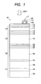
- FIG. 1 is a schematic cross sectional view of an embodiment of stacked photovoltaic element according to the invention, showing its configuration.
- the stacked photovoltaic element 101 contains a structure formed by sequentially arranging a metal layer 103, a lower transparent conductive layer 104, a first n-layer 105 of non-single-crystal silicon, a first i-layer 106 of microcrystal silicon, a first p-layer 108 of non-single-crystal silicon, a second n-layer 109 of non-single-crystal silicon, a second i-layer 110 of microcrystal silicon and a second p-layer 112 of non-single-crystal silicon on a support body 102.
- the structure additionally has a third n-layer 113 of non-single-crystal silicon, a third i-layer 114 of amorphous silicon and third p-layer 115 of non-single-crystal and an upper transparent conductive layer 116 on and in contact with the second p-layer 112.
- a metal plate such as stainless steel plate or a glass plate is used for the support body 102.
- the metal layer 103 is laid on the support body 102 by evaporation, sputtering or electro-deposition.
- the metal layer 103 may have a multilayer structure of different metals. In any case, however, it is desirable that the metal layer 103 has a surface of Ag, Al, Cu or some other metal having a high reflectance at the side opposite to the support body 102.
- a lower transparent conductive layer 104 of ZnO, SnO 2 In 2 O 3 , ITO or the like is laid on the metal layer 103 typically by sputtering, CVD or electro-deposition.
- the surface of the metal layer and that of the lower transparent conductive layer are made to show a texture-like appearance in order to achieve a light-confining effect and the angle of inclination in micro-regions of the order of sub-microns on the surfaces is not less than 20 degrees and not more than 40 degrees.
- the work obtained by laying a metal layer 103 and a lower transparent conductive layer 104 on a support body 102 is referred to as substrate 121 herein.
- substrate 121 The work obtained by laying a metal layer 103 and a lower transparent conductive layer 104 on a support body 102 is referred to as substrate 121 herein.
- a first n-layer 105 of a-Si:H:P thin film, a phosphor-containing first i-layer 106 of ⁇ c-Si:H thin film, a first pi-layer 107 of a-Si:H thin film, a first p-layer 108 of a-Si:H:B or ⁇ c-Si:H:B are sequentially formed on the substrate 121 by CVD.
- the multilayer structure including the above four layers is referred to as bottom cell 122.
- a second n-layer 109 of a-Si:H:P thin film, a phosphor -containing second i-layer 110 of ⁇ c-Si:H thin film, a second pi-layer 111 of a-Si:H thin film, a second p-layer 112 of a-Si:H:B or ⁇ c-Si:H:B are sequentially formed on the bottom cell 122 also by CVD.
- the multilayer structure including the above four layers is referred to as middle cell 123.
- a third n-layer 113 of a-Si:H:P thin film, a third i-layer 114 of a-Si:H thin film and a third p-layer 115 of a-Si:H:B or ⁇ c-Si:H:B are sequentially formed on the middle cell 123 also by CVD.
- the multilayer structure including the above three layers is referred to as top cell 124.
- first pi-layer 107 and the second pi-layer 111 are not indispensable for the purpose of the present invention, they are preferably provided because the pi interface characteristic and also Voc and FF are improved when they are arranged.
- Each of the layers of the bottom cell 122, the middle cell 123 and the top cell 124 is made of high quality thin film that contains hydrogen and in which defective levels such as dangling bonds are almost completely compensated.
- an upper transparent conductive layer 116 of ZnO, SnO 2 In 2 O 3 , ITO or the like is formed on the top cell 124 by sputtering or resistance heating.
- the use of ITO is particularly desirable as material of the upper transparent conductive layer. It is desirable to make the upper transparent conductive layer have a film thickness of about 70 nm and the reflectance of the layer become lowest at and near the wavelength of 520 nm.
- a comb-shaped current collecting electrode 117 is formed on the upper transparent conductive layer 116. It is desirable that the current collecting electrode 117 is prepared by forming an Ag clad layer 119 and a carbon clad layer 120 around a Cu wire 118 by application and fusion-bonding the prepared current collecting electrode 117 to the upper transparent conductive layer.
- the above-described metal layer 103, the lower transparent conductive layer 104, the bottom cell 122, the middle cell 123, the top cell 124 and the upper transparent conductive layer 116 are formed by a roll-to-roll method for the purpose of improving the productivity.
- the i-layers may not necessarily be of intrinsic conductive type. They may be of weak p-type or weak n-type conductive type.
- the inventor of the present invention found a phenomenon that the spectral sensitivity of a single cell having an i-layer of ⁇ c-Si:H thin film can be controlled for a specific wavelength by adjusting the phosphor concentration of the i-layer of the single cell and applied this phenomenon to current balance adjustment of a triple cell. Therefore, firstly the phenomenon will be described below.
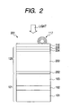
- FIG. 2 is a schematic cross sectional view of a photovoltaic element 201 comprising a single cell 125 having an i-layer of ⁇ c-Si:H thin film.
- the single cell 125 has a single pin junction including an i-layer 203 of ⁇ c-Si:H thin film.
- the materials and the forming processes of the layers are same as those described above by referring to FIG. 1.
- An upper transparent conductive layer 116 is laid on the p-layer 205.
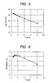
- FIGS. 3 through 6 are graphs illustrating the relationships between the phosphor concentration of the i-layer and various characteristics of the single cell of FIG. 2 obtained by controlling the volume of PH 3 gas introduced simultaneously with SiH 4 gas, SiF 4 gas and H 2 gas into the vacuum chamber that was used for forming the i-layer 203 of the single cell by CVD.
- the relationship between the P concentration in the i-layer and Voc see FIG. 3
- the relationship between the P concentration in the i-layer and FF show a substantially same tendency. More specifically, both Voc and FF increase monotonically until the P content ratio gets to 1ppm from the lower side and the rate of increase is reduced beyond 1ppm of the P content ratio until they become saturated.
- Jsc decreases monotonically as the P concentration in the i-layer increases (see FIG. 5).
- the conversion efficiency monotonically increases until the P concentration gets to 2ppm from the lower side and then slowly and monotonically decreases beyond 2ppm of the P concentration (see FIG. 6). It will be appreciated from the graphs that the highest conversion efficiency is realized when the P concentration in the i-layer of ⁇ c-Si:H thin film of a single cell is found at or near 2ppm.
- both the i-layer of ⁇ c-Si:H thin film of the bottom cell and that of the middle cell of a stacked photovoltaic element according to the invention contain phosphor, the two cells show a high FF value and therefore the triple cell including the two cells also shows a high FF value.
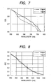
- the bottom cell shows very high Voc and FF values due to the phosphor it contains. While the Jsc value decreases as the phosphor concentration rises as seen from FIG. 5, the spectral sensitivity relative to light with a wavelength range above 800 nm is sufficient for the bottom cell as seen from FIG. 8. Additionally, the spectral sensitivity of the middle cell is sufficient for a middle cell as seen from FIG. 7 because the phosphor concentration of the middle cell is low.
- the method of adjusting the current balance of the bottom cell and that of the middle cell is normally employed under the conditions where the highest efficiency is obtained.
- the level of spectral sensitivity that is required to the middle cell can be controlled by controlling the P concentration in the i-layer of ⁇ c-Si:H thin film.
- ⁇ c-Si:H thin film that is used for photovoltaic elements and phosphor is deposited exclusively in amorphous regions or on crystal grain boundaries.
- Many dangling bonds of silicon exist on crystal grain boundaries of ⁇ c-Si:H thin film in which amorphous regions are practically not found.
- dangling bonds are quite rare on crystal grain boundaries of ⁇ c-Si:H thin film in which many amorphous regions exist because gaps separating crystals are surrounded by amorphous regions.
- the i-layers of ⁇ c-Si:H thin film in a photovoltaic element according to the invention are basically in such a state.
- ⁇ c-Si:H thin film is formed by CVD (gas phase chemical reaction)
- the above reaction does not take place on the outermost surface of the film but it is a solid phase reaction that takes place in the thin film forming process.
- PH 3 gas is used as raw material gas when phosphor is introduced into ⁇ c-Si:H thin film, PH 2 * is excited in plasma so that probably the following reactions take place on the outermost surface.
- the phosphor content ratio of the i-layer of the bottom cell and that of the i-layer of the middle cell of a stacked photovoltaic element according to the invention are R1 and R2 respectively, preferably the relationship of R1 and R2 is defined by the formula of 0.1ppm ⁇ R2 ⁇ R1 ⁇ 4ppm.
- the i-layer of the' middle cell contains phosphor only to a small extent, it is possible to improve the spectral sensitivity relative to the wavelength range between 550 nm and 800 nm when the i-layer has a small film thickness. Then, additionally, light can get to the bottom cell to a large extent because of the small film thickness of the i-layer of the middle cell, it is also possible to improve the spectral sensitivity of the bottom cell.
- the i-layer of the bottom cell contains phosphor to a relatively large extent, it is possible to achieve a high open-circuit voltage and a high FF value so that the spectral sensitivity to the wavelength range between 800 nm and 1100 nm of the bottom cell is sufficiently high.
- the i-layer of the middle cell does not contain amorphous regions to a large extent, it is free from photo-degradation. Furthermore, since the film thickness is not controlled to adjust the delicate current balance, the conversion efficiency does not fluctuate if the film thickness of the i-layer of the middle cell and that of the bottom cell unpredictably come to show fluctuations during the process of forming them.
- a photovoltaic element as shown in FIG. 1 was prepared in this example. Firstly, a substrate was prepared for a photovoltaic element according to the invention by using systems as shown in FIGS. 9 and 10.
- FIG. 9 is a schematic illustration of a roll-to-roll type thin film forming system that is adapted to continuously form different thin films on a belt-shaped support body 302 respectively in different spaces.
- reference symbols 303, 304 and 305 denote vacuum chambers for forming thin film by DC sputtering.
- Different thin films can be formed by using different target materials.
- a Ti target, an Ag target and a ZnO target are used respectively in the vacuum chambers 303, 304 and 305 so that a Ti layer, an Ag layer and a ZnO layer can be formed sequentially on a support body.
- a heater 310 is arranged to heat the belt-shaped support body 302 from the rear surface thereof whereas a target 311 and an electrode 312 that is connected to the target are arranged at the opposite side relative to the belt-shaped support body 302.
- a DC power source 313 is connected to each of the electrodes 312.
- a gas supply pipe 314 is connected to each of the vacuum chamber so that raw material gas can be introduced into the vacuum chamber from a gas supply unit (not shown).
- an exhaust pipe 315 is connected to each of the vacuum chamber so that the inside of the vacuum chamber can be evacuated by means of a vacuum pump (not shown) to produce vacuum therein.
- a belt-shaped support body 302 is wound around the drum 306 to form a roll and set in position in the inside of vacuum chamber 307.
- the belt-shaped support body 302 is pulled out at the free end thereof and made to move through the vacuum chambers 303, 304, 305 and become wound around the drum 309 arranged in the inside of vacuum chamber 308.
- the vacuum chambers and the vacuum paths 317 connecting the vacuum chambers are evacuated by means of the vacuum pumps by way of the respective exhaust pipes connecting the vacuum chambers and the vacuum pumps respectively.
- the belt-shaped support body 302 is heated to a predetermined temperature level by means of the heaters 310.
- Ar gas is introduced into the vacuum chambers from the respective gas supply pipes at a flow rate of 50 sccm and the internal pressure is held to 3 Pa.
- a voltage is applied to the electrodes of the vacuum chambers to generate plasma 316 in the vacuum chambers.
- the DC power and the moving speed of the belt-shaped support body are adjusted to make the thicknesses of the Ti layer, the Ag layer and the ZnO layer respectively equal to 50 nm, 800 nm and 200 nm.
- a metal layer 103 is formed by the laminate of the Ti layer and the Ag layer. The thin film forming process using the system of FIG. 9 was terminated when a metal layer and a ZnO layer were formed to an effective length of 100m on the belt-shaped support body.
- FIG. 10 is a schematic illustration of a system 401 adapted to form a ZnO layer on the ZnO layer formed by the sputtering system 301 of FIG. 9 by means of a roll-to-roll type electro-deposition method.
- the system 401 comprises an electro-deposition tank 403 for forming a ZnO layer by electro-deposition, a washing water tank 404, an air knife 407 and a heater 410.
- the electro-deposition tank 403 is filled with an electro-deposition producing solution 416 and a zinc electrode 414 is arranged vis-à-vis the support body 402, on which the ZnO layer is formed in the sputtering system of FIG. 9, and connected to a DC power source 413.
- the film thickness of the ZnO layer that is formed in the system 401 can be controlled by way of the moving speed of the support body 402 and the current density of the electric current flowing to the electrode 414.
- the washing water tank 404 is filled with pure water 417 and connected to a pure water supply unit 415.
- a support body 402 on which a ZnO layer is formed by the sputtering system of FIG. 9 is wound around the drum 406 to form a roll. Then, it is pulled out at the free end thereof and made to move through the electro-deposition producing solution 416, the pure water 417, the air knife 407 and the heater 410 and become wound around drum 409. As the drums 406 and 409 are driven to rotate, the support body 402 is moved from left to right so that different treatments can be conducted simultaneously in respective different spaces.
- the electro-deposition producing solution 416 an aqueous solution of 0.2 mol/L of zinc nitrate and 0.1 g/L of dextrin is heated to 80°C by solution heater 411 in a controlled manner.
- the power source 413 is controlled so as to produce an electric current of 8.0 mA/cm 2 that flows to the electrode 414.
- the electro-deposition producing solution adhering to the surface of the ZnO film and the rear film of the support body is washed off in the pure water tank 404. Additionally, pure water drops are evaporated by means of the air knife 407 and the heater 410.
- the support body 402 is heated by the heater 410 to about 120°C.
- a ZnO layer was formed continuously while taking up the support member 402 by the drum 409. The ZnO layer forming process using the electro-deposition system of FIG. 10 was terminated when a substrate was formed to an effective length of 100m.
- a ZnO layer was formed by means of the above described process to a film thickness of 2.6 ⁇ m. Since a ZnO layer had been formed on the substrate to a film thickness of 0.4 ⁇ m in advance by means of the sputtering system of FIG. 9, the film thickness of the lower transparent conductive layer 104 of ZnO layer is 3.0 ⁇ m.
- the procedure for forming the substrate 121 is described above.
- the light reflection characteristics of the prepared substrate 121 were examined to find that the regular reflection was 90% and the diffused reflection was 80%, while the hazing ratio was 89% and hence that the substrate 121 was a high quality texture substrate.
- FIG. 11 is a schematic illustration of a system to be used for forming a bottom cell 122, a middle cell 123 and a top cell 124 by means of a roll-to-roll type CVD method on the substrate 121 that is formed by using the system of FIGS. 9 and 10.
- the system 501 comprises vacuum chambers 502, 503, 504, 505, 506, 507, 508, 509 and vacuum paths 510 linking the vacuum chambers.
- the vacuum chamber 508 is used to feed out the substrate, which is wound around a drum 511 to form a roll, to the downstream vacuum chambers and the vacuum chamber 509 is used to take up the substrate, which carries a bottom cell and a middle cell, around a drum 512.
- the vacuum chamber 502 is a chamber for forming the first and second n-layers and the vacuum chambers 503, 504, 505 are chambers for forming the first and second i-layers, while the vacuum chamber 506 is a chamber for forming the first and second pi-layers and the vacuum chamber 507 is a chamber for forming the first and second p-layers.
- a raw material gas supply pipe 517 and an exhaust pipe 518 are connected to each of the vacuum chambers and a path gas supply pipe 519 is connected to each of the vacuum paths. As path gas is supplied to the path gas supply pipes 519 at a predetermined rate, mutual diffusion of raw material gas can be suppressed to take place among the vacuum chambers.
- a raw material gas supply unit (not shown) is connected to each of the raw material gas supply pipes 517, while each of the vacuum chambers 502, 503, 504, 505, 506, 507 is provided in the inside thereof with a heater 513 for heating the substrate from the rear surface thereof and an electrode 514 for generating high frequency plasma 515.
- the electrodes 514 are connected to respective high frequency power sources 522, 523, 524, 525, 526, 527.
- a substrate 121 which is wound around a drum 511 to form a roll, is pulled out at the free end thereof and made to pass through the vacuum paths and the vacuum chambers sequentially so that it is taken up by and wound around drum 512.
- the vacuum chambers and the vacuum paths are evacuated to produce vacuum therein to a predetermined pressure level by means of the vacuum pumps connected to the respective vacuum chambers.
- the substrate 121 is heated to a predetermined temperature level by means of the heaters 513 and the drums 511, 512 are driven to rotate in order to start conveying the substrate 121.
- H 2 gas is made to flow at a rate of about 2slm to each of the path gas supply pipes and predetermined raw material gas is introduced into each of the vacuum chambers from the raw material gas supply pipe connected to the vacuum chamber. Then, the conductance valves (not shown) of the vacuum chambers are operated for adjustment for the purpose of holding the internal pressure of each of the vacuum chambers to a predetermined pressure level. Additionally, high frequency power is supplied to the electrode 514 arranged in the inside of each of the vacuum chambers at a predetermined rate to generate high frequency plasma.
- the thin film forming process using the system of FIG. 11 is terminated when a bottom cell 122 is formed to an effective length of 100m on the substrate 121. Table 1 below shows the conditions for forming the layers of the bottom cell 122 of a photovoltaic element according to the invention.
- a middle cell 123 was prepared by using a system as shown in FIG. 11 and following similar procedures.
- Table 1 below also shows the conditions for forming the layers of the middle cell 123 of a photovoltaic element according to the invention.
- a top cell 124 was prepared by using a system as shown in FIG. 11 and following similar procedures.
- Table 1 below also shows the conditions for forming the layers of the top cell 124 of a photovoltaic element according to the invention.
- the Ti target was replaced by an ITO target with 3 wt% of SnO 2 and an upper transparent electro-conductive layer 116 of ITO was formed to a film thickness of 70 nm by following similar procedures.
- the 100m long photovoltaic element formed on the belt-shaped support body was cut to 25 cm long pieces to produce 400 photovoltaic elements.
- material A is amorphous silicon and material M is microcrystal silicon.
- the photovoltaic elements were subjected to a shunt passivation process. More specifically, potassium hydroxide was dissolved to a small extent as pH regulator in 1% aqueous solution of sulfuric acid to make the aqueous solution show a pH value of 1.7. Then, each of the photovoltaic elements having a length of 25 cm were immersed in the aqueous solution.
- a positive electrode was arranged vis-à-vis the upper transparent conductive layer 116 and a sinusoidal wave voltage having the highest voltage of 3V, the lowest voltage of 0V and a cycle period of 1 second was applied to the electrode to remove the upper transparent conductive layer at and near the short-circuit section.
- the low illuminance Voc at 200 lux of each and every photovoltaic element subjected to this process was above 1.0(V) and no short-circuited photovoltaic element was found.
- wire grids formed by applying an Ag clad layer and a carbon clad layer to Cu wires were arranged at regular intervals of 5 mm and fusion-bonded to the upper transparent conductive layer 116. Then, the ends of the wire grids were connected to Cu tabs that were coated with Ag to produce a current collecting electrode 117.
- FIG. 12 is a schematic view of one of the photovoltaic elements as viewed from the light receiving side thereof.
- the characteristics of the photovoltaic elements were observed by means of a solar simulator adjusted to AM1.5 and 100 mW/cm 2 .
- Table 2 shows the average values obtained by observing the characteristics of the 400 photovoltaic elements.
- the phosphor content ratios of the first i-layer and the second i-layer were observed by means of SIMS to find that they were respectively 1.6ppm and 0.6ppm relative to silicon.
- a total of 400 triple cells were prepared as in Example 1 except that the phosphor concentration in the i-layer of the middle cell was made equal to its counterpart of the i-layer of the bottom cell and the current balance was adjusted by raising the film thickness of the i-layer of the middle cell.
- the characteristics of the photovoltaic elements were observed by means of a solar simulator.
- Table 2 also shows the average values obtained by observing the characteristics of the 400 photovoltaic elements of this example for comparison. conversion efficiency (%) Voc (V) Jsc (mA/cm 2 ) FF
- the Jsc dispersion of the 400 specimens of Example for Comparison 1 was more remarkable than the Jsc dispersion of the 400 specimens of Example 1. While the yield factor of Example 1 was 97%, that of Example for Comparison 1 was as low as 90%. It was found that the Jsc dispersion of Example for Comparison 1 was attributable to instability of electric discharges. As a result, it was also found that photovoltaic elements according to the invention practically do not show any dispersion of conversion efficiency and can be manufactured with a high yield factor so that a current balance adjustment method according to the invention is advantageous relative to comparable known methods.
- Photovoltaic elements were prepared as in Example 1 except that a substrate having a 2.8 ⁇ m thick ZnO layer formed by sputtering was used as lower transparent conductive layer 104 and hence no ZnO layer was formed by electro-deposition. As a result, characteristics and a yield factor as excellent as those of Example 1 were observed.
- Photovoltaic elements were prepared as in Example 1 except that PH 3 gas was caused to flow into the vacuum chambers at a rate of 0.01 sccm during the step of forming the i-layer of the bottom cell. As a result, characteristics and a yield factor as excellent as those of Example 1 were observed.
- a stacked photovoltaic element contains a structure formed by sequentially arranging a metal layer 103, a lower transparent conductive layer 104, a first n-layer 105 of non-single-crystal silicon, a first i-layer 106 of microcrystal silicon, a first p-layer 108 of non-single-crystal silicon, a second n-layer 109 of non-single-crystal silicon, a second i-layer 110 of microcrystal silicon and a second p-layer 112 of non-single-crystal silicon on a support body 102.
- the first i-layer 106 and the second i-layer 110 are made to contain phosphor and the content ratio R1 of phosphor to silicon of the first i-layer 106 and the content ratio R2 of phosphor to silicon of the second i-layer 110 are defined by the formula of R2 ⁇ R1. With this arrangement, photovoltaic elements showing a high conversion efficiency can be manufactured with a high yield factor.
Landscapes
- Photovoltaic Devices (AREA)
Abstract
A stacked photovoltaic element contains a structure formed by sequentially arranging a metal layer 103, a lower transparent conductive layer 104, a first n-layer 105 of non-single-crystal silicon, a first i-layer 106 of microcrystal silicon, a first player 108 of non-single-crystal silicon, a second n-layer 109 of non-single-crystal silicon, a second i-layer 110 of microcrystal silicon and a second player 112 of non-single-crystal silicon on a support body 102. The first i-layer 106 and the second i-layer 110 are made to contain phosphor and the content ratio R1 of phosphor to silicon of the first i-layer 106 and the content ratio R2 of phosphor to silicon of the second i-layer 110 are defined by the formula of R2 < R1. With this arrangement, photovoltaic elements showing a high conversion efficiency can be manufactured with a high yield factor. <IMAGE>
Description
This invention relates to a photovoltaic
element and, more particularly, it relates to a solar
battery. More particularly, the present invention
relates to an improvement to the conversion
efficiency and the yield factor of stacked solar
batteries having two or more than two pin junctions
formed by using i-layers of microcrystal silicon (µc-Si:H)
thin film. This invention also relates to a
current balance adjustment method for each component
cell of a stacked solar battery formed by using i-layers
of microcrystal silicon thin film.
In recent years, thin film solar batteries
formed by using a silicon based non-single-crystal
(and non-polycrystalline) semiconductor have been
attracting attention from the viewpoint of
encouraging the use of electric power generated by
solar energy because such a solar battery can be
formed on a relatively less expensive substrate such
as a glass or metal sheet to make it show a large
surface area and a small thickness if compared with a
solar battery formed by using a single-crystal or
polycrystalline semiconductor and hence large area
solar batteries can be manufactured at low cost.
However, thin film solar batteries have not
been used on a large scale because the conversion
efficiency of thin film solar batteries is low and
they are subject to photo-degradation when compared
with crystalline silicon solar batteries. Therefore,
efforts have been and are being paid to improve the
performance of thin film solar batteries.
For example, researches for utilizing a
material showing a large long-wavelength absorption
coefficient relative to amorphous silicon for i-layers
of solar batteries are intensively under way.
Unlike amorphous thin film such as a-SiGe:H, for
instance, µc-Si:H is practically free from photo-degradation
and, additionally, does not require the
use of expensive raw material gas such as germane gas
(GeH4). While µc-Si:H thin film does not have an
absorption coefficient as high as a-SiGe:H thin film,
it is possible for a µc-Si:H single cell to obtain a
short circuit current (Jsc) that is stronger than
that of an a-SiGe:H single cell when the film
thickness of the i-layer is made greater than 2 µm.
For instance, MRS Symposium Proceeding, Vol.
420, Amorphous Silicon Technology 1996, pp. 3-13, "On
the Way towards High Efficiency Thin-Film Silicon
Solar Cells by the Micromorph Concept", by J. Meier
et al. describes that the authors achieved a
conversion efficiency of 7.7% in a single cell having
a single pin junction, where the i-layer was made of
µc-Si:H, that was prepared by means of VHF plasma CVD,
using a frequency of 110 MHz. The single cell had a
remarkable advantage that it was free from photo-degradation.
The above document also describes that
the authors also achieved a conversion efficiency of
13.1% in a stacked cell (double cell) prepared by
additionally forming another pin junction, where the
i-layer was made of amorphous silicon based thin film
(a-Si:H).
Japan Journal of Applied Physics Vol. 36 (1997),
pp. L569-L572, Part 2, No. 5A, "Optical Confinement
Effect for below 5 µm Thick Film Poly-Si Solar Cell
on Glass Substrate", by Kenji Yamamoto et al., Kaneka
Corporation describes that the authors achieved a
conversion efficiency of 9.8% in a single cell having
a pin junction of poly-Si and µc-Si. The i-layer of
the cell was 3.5 µm, which is thin for a poly-Si
single cell, although the short circuit current (Jsc)
was 26 mA/cm2, which is relatively large. The above
document also describes that the authors also
achieved a conversion efficiency of 12.8% in a
stacked cell (double cell) prepared by additionally
forming another pin junction, where the i-layer was
made of amorphous silicon based thin film (a-Si:H).
Furthermore, 26th Photovoltaic Specialists
Conference 1997, "Thin Film Poly-Si Solar Cell with
Star Structure on Glass Substrate Fabricated at Low
Temperature", Kenji Yamamoto, Masashi Yoshimi et al.
describes that the authors achieved a post-photo-degradation
conversion efficiency of 11.5% in a
stacked cell (triple cell) having three pin junctions,
where the i-layers were made of a-Si:H thin film /µc-Si:H
thin film / µc-Si:H thin film respectively.
Japanese Patent Application Laid-Open No. H11-251610
discloses a technique of turning an i-layer of
µc-Si:H thin film into a weak n-type or p-type layer
by adding a valence electron control agent to a
slight extent.
Japanese Patent Application Laid-Open No. H11-310495
discloses a technique of adding phosphor to an
i-layer of µc-Si:H thin film to a ratio of 1ppm .
Japanese Patent Application Laid-Open No. H11-317538
discloses a technique of adding phosphor-containing
gas to the raw material gas to a ratio
between about 10ppm and about 1,000ppm in order to
form an n- layer in a photovoltaic element having a
p+n-n+ junction of µc-Si:H thin film.
Japanese Patent Application Laid-Open No. H11-243218
discloses a photovoltaic element comprising a
bottom cell and a middle cell each formed by using an
i-layer of µc-Si:H thin film and a top cell formed by
using an i-layer of a-Si:H.
It is well known to form a rear surface
reflection-layer in order to return sun light that
was not absorbed by a thin film semiconductor layer
back to the thin film semiconductor layer by
controlling the surface profile of a substrate and
raising its reflectance so as to effectively utilize
incident light. For example, when causing sun light
to strike the surface of a thin film semiconductor
layer, a remarkable internal light confinement effect
is realized to improve the short circuit current by
forming a layer of a metal having a high reflectance
such as silver (Ag) or aluminum (Al) on a substrate,
forming a transparent electro-conductive layer made
of ZnO or SnO2 and having appropriate surface
undulations thereon, and forming a photovoltaic layer
further thereon. For instance, as disclosed in
Japanese Patent Application Laid-Open No. 2000-22189,
a transparent electro-conductive layer of ZnO can be
formed by combining sputtering and electro-deposition.
Photovoltaic elements (to be referred to simply
as cells hereinafter) having an i-layer of µc-Si:H
thin film that can produce a short circuit current of
30 mA/cm2 or more are currently available. Such cells
have properties that cannot be obtained by cells
having an i-layer of a-SiGe:H thin film.
Additionally, while cells having an i-layer of a-SiGe:H
thin film are accompanied by a serious problem
of photo-degradation, some cells having an i-layer of
µc-Si:H thin film are free from the problem of photo-degradation.
Furthermore, while cells having an i-layer
of a-SiGe:H thin film need to be formed by
using expensive gas such as GeH4, cells having an i-layer
of µc-Si:H thin film can be formed without
using such expensive raw material gas. Thus, cells
having an i-layer of
µc-Si:H thin film provides a number of advantages.
On the other hand, however, photovoltaic
elements having an i-layer of µc-Si:H thin film are
accompanied by a problem that the conversion
efficiency of a single cell that has a single pin
junction is as low as about 10%. The inventor of the
present invention prepared a stacked cell (double
cell) comprising a light receiving top cell having an
i-layer of a-Si:H thin film and a rear side bottom
cell having an i-layer of µc-Si:H thin film and
adjusted the current balance of each component cell.
As a result, the initial conversion efficiency was as
high as 12%.
However, double cells of the above-described
type were accompanied by a serious problem of photo-degradation.
As a result of research efforts, it was
found that the photo-degradation was caused mainly
because the film thickness of the i-layer of the top
cell had been increased to 400 nm as a result of the
current balance adjustment. Thus, the inventor of
the present invention prepared a stacked cell (triple
cell) comprising a top cell having an i-layer of a-Si:H
thin film, a middle cell having an i-layer of
µc-Si:H thin film arranged under the top cell and a
bottom cell having an i-layer of µc-Si:H thin film
arranged under the middle cell and conducted an
experiment for suppressing photo-degradation by
reducing the film thickness of the i-layer of a-Si:H
thin film.
To adjust the current balance of a stacked cell,
it is desirable to adjust the band gap of the i-layer
of each component cell so as to minimize the overlap
of the spectral sensitivity curves of the component
cells. For this purpose, it is then desirable to lay
i-layers having different band gaps one on the other
in the descending order of band gaps. In other words,
an i-layer having a large band gap needs to be
arranged at the light receiving side, while an i-layer
having a small band gap needs to be arranged at
the rear side. Additionally, the current balances of
the component cells need to be made uniform by
adjusting the film thickness of the i-layer of each
component cell. The uniform current value to be
achieved is the value obtained by dividing the
largest Jsc value that is obtained for a single cell
by the number of cells in the stack (the number of
pin junctions).
In the case of a double cell prepared in a
manner as described above, where the cells are
connected in series, sun light can be effectively
converted into electricity because the open-circuit
voltage of the top cell and that of the bottom cell
show a large difference. Therefore, the current
balances can be adjusted simply by adjusting the film
thicknesses.
The inventor of the present invention conducted
an experiment of changing the band gap of the
component cells having an i-layer of a triple cell
comprising two i-layers of µc-Si:H thin film when
adjusting the current balance of each component cell.
As a result, it was possible to change the open-circuit
voltage of each i-layer of µc-Si:H thin film
from 0.40 eV to 0.62 eV. However, a cell whose open-circuit
voltage could be changed from 0.40 eV to 0.47
eV showed only a small short-circuit current in spite
of the low open-circuit voltage. Such a cell cannot
find practical applications. A cell whose open-circuit
voltage could be changed from 0.55 eV to 0.62
eV, on the other hand, was subject to photo-degradation
to a large extent. Such a cell cannot
find practical applications either. In other words,
the range of open-circuit voltage that can be used in
the middle cell and the bottom cell of a triple cell
of the above-described type is very narrow and
limited to between 0.48 eV and 0.54 eV to provide
limitations to band gap adjustment.
Additionally, adjustment of current balance
needs to mainly rely on adjustment of film thickness.
When adjustment of current balance is limited to
adjustment of film thickness, it is not possible to
achieve a large open-circuit voltage for a triple
cell and the wavelength selectivity of the spectral
sensitivity spectrum of each component cell is
practically lost. Then, such a cell cannot provide
effective photoelectric conversion. Additionally, it
is difficult to control the film thickness of each
component cell so that the generated electric current
of the bottom cell fluctuates as the film thickness
of the middle cell fluctuates and vice versa. Then,
as a result, the current balance is lost to reduce
the conversion efficiency.
A triple cell having i-layers of µc-Si:H thin
film as described in Japanese Patent Application
Laid-Open No. H11-243218 is accompanied by the same
problems.
In view of the above identified problems, it is
therefore an object of the present invention to
dissolve the above problems by providing a new
current balance adjustment method for adjusting the
current balance of a stacked cell (triple cell in
particular) having two or more than two i-layers of
µc-Si:H thin film. It is another object of the
present invention to provide a photovoltaic element
whose current balance is adjusted by the adjustment
method.
The inventor of the present invention found a
phenomenon that the spectral sensitivity of a single
cell having an i-layer of µc-Si:H thin film can be
controlled for a specific wavelength by adjusting the
phosphor (P) content ratio of the i-layer of the
single cell and got to the present invention by
applying the above phenomenon to current balance
adjustment of a stacked cell (triple cell in
particular) with intensive research efforts.
In an aspect of the present invention, there is
provided a current balance adjustment method for a
stacked photovoltaic element containing a structure
formed by sequentially arranging a first n-layer of
non-single-crystal silicon, a first i-layer
microcrystal silicon, a first p-layer of non-single-crystal
silicon, a second n-layer of non-single-crystal
silicon, a second i-layer of microcrystal
silicon and a second p-layer of non-single-crystal
silicon, said method comprising causing said first i-layer
and said second i-layer to contain spectral
sensitivity adjusting atoms and adjusting the
current balance by adjusting the concentration of
spectral sensitivity adjusting atoms.
Preferably, said spectral sensitivity adjusting
atoms are phosphor (P) atoms.
In another aspect of the invention, there is
provided a photovoltaic element containing a
structure formed by sequentially arranging a metal
layer, a lower transparent conductive layer, a first
n-layer of non-single-crystal silicon, a first i-layer
of microcrystal silicon, a first p-layer of
non-single-crystal silicon, a second n-layer of non-single-crystal
silicon, a second i-layer of
microcrystal silicon and a second p-layer of non-single-crystal
silicon on a support body, said first
i-layer and said second i-layer containing phosphor
(P) and the content ratio R1 of phosphor to silicon
of the first i-layer and the content ratio R2 of
phosphor to silicon of the second i-layer is defined
by the formula of
R2 < R1.
Preferably, said structure is formed by
additionally and sequentially laying a third n-layer
of non-single-crystal silicon, a third i-layer of
amorphous silicon and third p-layer of non-single-crystal
silicon and an upper transparent conductive
layer of ITO on and in contact with said second p-layer.
Preferably, the relationship of said content
ratios R1 and R2 is defined by the formula of
0.1ppm < R2 < R1 < 4ppm.
With the current balance adjustment method
according to the invention, the spectral sensitivity
of the stacked cell relative to a specific wavelength
is adjusted by causing the i-layers of µc-Si:H thin
film to contain spectral sensitivity adjusting atoms
and adjusting the current balance of the stacked cell.
The mechanism involved in the method will be
described in greater detail hereinafter. With the
current balance adjustment method according to the
invention, it is possible to raise or lower the
sensitivity of the stacked cell relative to light
with a wavelength band between 550 nm and 800 nm
without changing the band gap of the i-layers by
adjusting the phosphor content ratio of the i-layers
of µc-Si:H thin film. The adjustment range is
modified by changing the phosphor content ratio
between about 0.1ppm and about 4ppm so that there is
no risk that the instability at the time of forming
the layers entails reduction in the conversion
efficiency and in the yield factor of stacked cells
of the type under consideration.
Now, the present invention will be described in
greater detail by referring to the accompanying
drawings that illustrate preferred embodiments of the
invention.
FIG. 1 is a schematic cross sectional view of
an embodiment of stacked photovoltaic element
according to the invention, showing its configuration.
Referring to FIG. 1, the stacked photovoltaic element
101 contains a structure formed by sequentially
arranging a metal layer 103, a lower transparent
conductive layer 104, a first n-layer 105 of non-single-crystal
silicon, a first i-layer 106 of
microcrystal silicon, a first p-layer 108 of non-single-crystal
silicon, a second n-layer 109 of non-single-crystal
silicon, a second i-layer 110 of
microcrystal silicon and a second p-layer 112 of non-single-crystal
silicon on a support body 102. The
structure additionally has a third n-layer 113 of
non-single-crystal silicon, a third i-layer 114 of
amorphous silicon and third p-layer 115 of non-single-crystal
and an upper transparent conductive
layer 116 on and in contact with the second p-layer
112.
A metal plate such as stainless steel plate or
a glass plate is used for the support body 102. The
metal layer 103 is laid on the support body 102 by
evaporation, sputtering or electro-deposition. The
metal layer 103 may have a multilayer structure of
different metals. In any case, however, it is
desirable that the metal layer 103 has a surface of
Ag, Al, Cu or some other metal having a high
reflectance at the side opposite to the support body
102. A lower transparent conductive layer 104 of ZnO,
SnO2 In2O3, ITO or the like is laid on the metal
layer 103 typically by sputtering, CVD or electro-deposition.
Preferably, the surface of the metal
layer and that of the lower transparent conductive
layer are made to show a texture-like appearance in
order to achieve a light-confining effect and the
angle of inclination in micro-regions of the order of
sub-microns on the surfaces is not less than 20
degrees and not more than 40 degrees.
The work obtained by laying a metal layer 103
and a lower transparent conductive layer 104 on a
support body 102 is referred to as substrate 121
herein. Then, a first n-layer 105 of a-Si:H:P thin
film, a phosphor-containing first i-layer 106 of µc-Si:H
thin film, a first pi-layer 107 of a-Si:H thin
film, a first p-layer 108 of a-Si:H:B or µc-Si:H:B
are sequentially formed on the substrate 121 by CVD.
The multilayer structure including the above four
layers is referred to as bottom cell 122.
Then, a second n-layer 109 of a-Si:H:P thin
film, a phosphor -containing second i-layer 110 of
µc-Si:H thin film, a second pi-layer 111 of a-Si:H
thin film, a second p-layer 112 of a-Si:H:B or µc-Si:H:B
are sequentially formed on the bottom cell 122
also by CVD. The multilayer structure including the
above four layers is referred to as middle cell 123.
Subsequently, a third n-layer 113 of a-Si:H:P
thin film, a third i-layer 114 of a-Si:H thin film
and a third p-layer 115 of a-Si:H:B or µc-Si:H:B are
sequentially formed on the middle cell 123 also by
CVD. The multilayer structure including the above
three layers is referred to as top cell 124.
While the first pi-layer 107 and the second pi-layer
111 are not indispensable for the purpose of
the present invention, they are preferably provided
because the pi interface characteristic and also Voc
and FF are improved when they are arranged.
Each of the layers of the bottom cell 122, the
middle cell 123 and the top cell 124 is made of high
quality thin film that contains hydrogen and in which
defective levels such as dangling bonds are almost
completely compensated.
Subsequently, an upper transparent conductive
layer 116 of ZnO, SnO2 In2O3, ITO or the like is
formed on the top cell 124 by sputtering or
resistance heating. The use of ITO is particularly
desirable as material of the upper transparent
conductive layer. It is desirable to make the upper
transparent conductive layer have a film thickness of
about 70 nm and the reflectance of the layer become
lowest at and near the wavelength of 520 nm.
Then, a comb-shaped current collecting
electrode 117 is formed on the upper transparent
conductive layer 116. It is desirable that the
current collecting electrode 117 is prepared by
forming an Ag clad layer 119 and a carbon clad layer
120 around a Cu wire 118 by application and fusion-bonding
the prepared current collecting electrode 117
to the upper transparent conductive layer.
It is desirable that the above-described metal
layer 103, the lower transparent conductive layer 104,
the bottom cell 122, the middle cell 123, the top
cell 124 and the upper transparent conductive layer
116 are formed by a roll-to-roll method for the
purpose of improving the productivity. Note that the
i-layers may not necessarily be of intrinsic
conductive type. They may be of weak p-type or weak
n-type conductive type.
The inventor of the present invention found a
phenomenon that the spectral sensitivity of a single
cell having an i-layer of µc-Si:H thin film can be
controlled for a specific wavelength by adjusting the
phosphor concentration of the i-layer of the single
cell and applied this phenomenon to current balance
adjustment of a triple cell. Therefore, firstly the
phenomenon will be described below.
FIG. 2 is a schematic cross sectional view of a
photovoltaic element 201 comprising a single cell 125
having an i-layer of µc-Si:H thin film. The single
cell 125 has a single pin junction including an i-layer
203 of µc-Si:H thin film. The materials and
the forming processes of the layers are same as those
described above by referring to FIG. 1. An upper
transparent conductive layer 116 is laid on the p-layer
205.
FIGS. 3 through 6 are graphs illustrating the
relationships between the phosphor concentration of
the i-layer and various characteristics of the single
cell of FIG. 2 obtained by controlling the volume of
PH3 gas introduced simultaneously with SiH4 gas, SiF4
gas and H2 gas into the vacuum chamber that was used
for forming the i-layer 203 of the single cell by CVD.
As seen from the graphs, the relationship between the
P concentration in the i-layer and Voc (see FIG. 3)
and the relationship between the P concentration in
the i-layer and FF (see FIG. 4) show a substantially
same tendency. More specifically, both Voc and FF
increase monotonically until the P content ratio gets
to 1ppm from the lower side and the rate of increase
is reduced beyond 1ppm of the P content ratio until
they become saturated. As for the relationship
between the P concentration in the i-layer and Jsc,
Jsc decreases monotonically as the P concentration in
the i-layer increases (see FIG. 5). As for the
relationship between the P concentration in the i-layer
and the conversion efficiency, the conversion
efficiency monotonically increases until the P
concentration gets to 2ppm from the lower side and
then slowly and monotonically decreases beyond 2ppm
of the P concentration (see FIG. 6). It will be
appreciated from the graphs that the highest
conversion efficiency is realized when the P
concentration in the i-layer of µc-Si:H thin film of
a single cell is found at or near 2ppm.
Since both the i-layer of µc-Si:H thin film of
the bottom cell and that of the middle cell of a
stacked photovoltaic element according to the
invention contain phosphor, the two cells show a high
FF value and therefore the triple cell including the
two cells also shows a high FF value. Particularly,
the bottom cell shows very high Voc and FF values due
to the phosphor it contains. While the Jsc value
decreases as the phosphor concentration rises as seen
from FIG. 5, the spectral sensitivity relative to
light with a wavelength range above 800 nm is
sufficient for the bottom cell as seen from FIG. 8.
Additionally, the spectral sensitivity of the middle
cell is sufficient for a middle cell as seen from FIG.
7 because the phosphor concentration of the middle
cell is low.
When a thin film that cannot change the band
gap is used as i-layer, the method of adjusting the
current balance of the bottom cell and that of the
middle cell is normally employed under the conditions
where the highest efficiency is obtained. However,
according to the present invention, the level of
spectral sensitivity that is required to the middle
cell can be controlled by controlling the P
concentration in the i-layer of µc-Si:H thin film.
It is believed that a large number of amorphous
regions normally exist in high quality µc-Si:H thin
film that is used for photovoltaic elements and
phosphor is deposited exclusively in amorphous
regions or on crystal grain boundaries. Many
dangling bonds of silicon exist on crystal grain
boundaries of µc-Si:H thin film in which amorphous
regions are practically not found. However, dangling
bonds are quite rare on crystal grain boundaries of
µc-Si:H thin film in which many amorphous regions
exist because gaps separating crystals are surrounded
by amorphous regions. The i-layers of µc-Si:H thin
film in a photovoltaic element according to the
invention are basically in such a state. However,
local levels attributable to dangling bonds and
structural strains will not be completely removed in
such a state. If phosphor is put into µc-Si:H thin
film in such a state, phosphor in crystals seem to
move to crystal boundaries and become bonded to
hydrogen atoms in amorphous regions in the process of
forming the photovoltaic element to consequently
inactivate dangling bonds.
Si* + P → Si-P*
Si-P* + 2H* → Si-PH2
While µc-Si:H thin film is formed by CVD (gas
phase chemical reaction), the above reaction does not
take place on the outermost surface of the film but
it is a solid phase reaction that takes place in the
thin film forming process.
However, since the small number of phosphor
atoms that are added to amorphous regions do not move
during the thin film forming process and hence
amorphous regions turn to slightly n-type regions, it
may be safe to assume that depletion is prevented
from occurring. Therefore, probably absorption takes
place only in absorbing regions of amorphous silicon
and the sensitivity to light with a wavelength range
between 550 nm and 800 nm is reduced to by turn
reduce the short circuit current as the phosphor
concentration increases. The fact that the dangling
bond density of high quality µc-Si:H thin film is
about 1 × 10¹⁵ to 1 × 10¹⁶ (1/cm3) and the
concentration of the added phosphor is of the order
of 1 × 10¹⁶ (1/cm3) also suggests the above described
mechanism.
If PH3 gas is used as raw material gas when
phosphor is introduced into µc-Si:H thin film, PH2*
is excited in plasma so that probably the following
reactions take place on the outermost surface.
PH3 → PH2* + H*
Si* + PH2* → Si-PH2
Meanwhile, when phosphor is added to a large
extent , phosphor atoms that do not take part in
compensation of dangling bonds on crystal grain
boundaries come to overflow in crystals so that the
crystals in the i-layer of µc-Si:H thin film seem to
turn to n-type crystals to suppress depletion of the
i-layer. Additionally, the large amount of phosphor
encourages amorphous regions to turn to n-type
regions and suppresses depletion similarly.
Therefore, this may be the reason why Jsc decreases
as the phosphor concentration increases.
If the phosphor content ratio of the i-layer of
the bottom cell and that of the i-layer of the middle
cell of a stacked photovoltaic element according to
the invention are R1 and R2 respectively, preferably
the relationship of R1 and R2 is defined by the
formula of
0.1ppm < R2 < R1 < 4ppm.
More specifically, since the i-layer of the'
middle cell contains phosphor only to a small extent,
it is possible to improve the spectral sensitivity
relative to the wavelength range between 550 nm and
800 nm when the i-layer has a small film thickness.
Then, additionally, light can get to the bottom cell
to a large extent because of the small film thickness
of the i-layer of the middle cell, it is also
possible to improve the spectral sensitivity of the
bottom cell.
Furthermore, since the i-layer of the bottom
cell contains phosphor to a relatively large extent,
it is possible to achieve a high open-circuit voltage
and a high FF value so that the spectral sensitivity
to the wavelength range between 800 nm and 1100 nm of
the bottom cell is sufficiently high.
Still additionally, since the i-layer of the
middle cell does not contain amorphous regions to a
large extent, it is free from photo-degradation.
Furthermore, since the film thickness is not
controlled to adjust the delicate current balance,
the conversion efficiency does not fluctuate if the
film thickness of the i-layer of the middle cell and
that of the bottom cell unpredictably come to show
fluctuations during the process of forming them.
Now, the present invention will be described
further by way of examples.
A photovoltaic element as shown in FIG. 1 was
prepared in this example. Firstly, a substrate was
prepared for a photovoltaic element according to the
invention by using systems as shown in FIGS. 9 and 10.
FIG. 9 is a schematic illustration of a roll-to-roll
type thin film forming system that is adapted
to continuously form different thin films on a belt-shaped
support body 302 respectively in different
spaces. In FIG. 9, reference symbols 303, 304 and
305 denote vacuum chambers for forming thin film by
DC sputtering. Different thin films can be formed by
using different target materials. A Ti target, an Ag
target and a ZnO target are used respectively in the
vacuum chambers 303, 304 and 305 so that a Ti layer,
an Ag layer and a ZnO layer can be formed
sequentially on a support body.
In the inside of each of the vacuum chambers, a
heater 310 is arranged to heat the belt-shaped
support body 302 from the rear surface thereof
whereas a target 311 and an electrode 312 that is
connected to the target are arranged at the opposite
side relative to the belt-shaped support body 302. A
DC power source 313 is connected to each of the
electrodes 312. Additionally, a gas supply pipe 314
is connected to each of the vacuum chamber so that
raw material gas can be introduced into the vacuum
chamber from a gas supply unit (not shown).
Furthermore, an exhaust pipe 315 is connected to each
of the vacuum chamber so that the inside of the
vacuum chamber can be evacuated by means of a vacuum
pump (not shown) to produce vacuum therein.
As drum 306 carrying the belt-shaped support
body 302 wound around it and take-up drum 309 are
driven to rotate, the belt-shaped support body 302 is
moved from left to right in FIG. 9 so that thin films
of different types can be formed simultaneously in
respective different spaces.
Now, the operating procedures of the above
system will be described below.
Firstly, a belt-shaped support body 302 is
wound around the drum 306 to form a roll and set in
position in the inside of vacuum chamber 307. The
belt-shaped support body 302 is pulled out at the
free end thereof and made to move through the vacuum
chambers 303, 304, 305 and become wound around the
drum 309 arranged in the inside of vacuum chamber 308.
The vacuum chambers and the vacuum paths 317
connecting the vacuum chambers are evacuated by means
of the vacuum pumps by way of the respective exhaust
pipes connecting the vacuum chambers and the vacuum
pumps respectively. Additionally, the belt-shaped
support body 302 is heated to a predetermined
temperature level by means of the heaters 310.
Then, Ar gas is introduced into the vacuum
chambers from the respective gas supply pipes at a
flow rate of 50 sccm and the internal pressure is
held to 3 Pa. Then, a voltage is applied to the
electrodes of the vacuum chambers to generate plasma
316 in the vacuum chambers. At this time, the DC
power and the moving speed of the belt-shaped support
body are adjusted to make the thicknesses of the Ti
layer, the Ag layer and the ZnO layer respectively
equal to 50 nm, 800 nm and 200 nm. A metal layer 103
is formed by the laminate of the Ti layer and the Ag
layer. The thin film forming process using the
system of FIG. 9 was terminated when a metal layer
and a ZnO layer were formed to an effective length of
100m on the belt-shaped support body.
FIG. 10 is a schematic illustration of a system
401 adapted to form a ZnO layer on the ZnO layer
formed by the sputtering system 301 of FIG. 9 by
means of a roll-to-roll type electro-deposition
method. The system 401 comprises an electro-deposition
tank 403 for forming a ZnO layer by
electro-deposition, a washing water tank 404, an air
knife 407 and a heater 410. The electro-deposition
tank 403 is filled with an electro-deposition
producing solution 416 and a zinc electrode 414 is
arranged vis-à-vis the support body 402, on which the
ZnO layer is formed in the sputtering system of FIG.
9, and connected to a DC power source 413. The film
thickness of the ZnO layer that is formed in the
system 401 can be controlled by way of the moving
speed of the support body 402 and the current density
of the electric current flowing to the electrode 414.
The washing water tank 404 is filled with pure water
417 and connected to a pure water supply unit 415.
Now, the procedures for forming a ZnO film by
means of the electro-deposition system 401 of FIG. 10
will be described below.
Firstly, a support body 402 on which a ZnO
layer is formed by the sputtering system of FIG. 9 is
wound around the drum 406 to form a roll. Then, it
is pulled out at the free end thereof and made to
move through the electro-deposition producing
solution 416, the pure water 417, the air knife 407
and the heater 410 and become wound around drum 409.
As the drums 406 and 409 are driven to rotate, the
support body 402 is moved from left to right so that
different treatments can be conducted simultaneously
in respective different spaces. As the electro-deposition
producing solution 416, an aqueous
solution of 0.2 mol/L of zinc nitrate and 0.1 g/L of
dextrin is heated to 80°C by solution heater 411 in a
controlled manner. The power source 413 is
controlled so as to produce an electric current of
8.0 mA/cm2 that flows to the electrode 414. The
electro-deposition producing solution adhering to the
surface of the ZnO film and the rear film of the
support body is washed off in the pure water tank 404.
Additionally, pure water drops are evaporated by
means of the air knife 407 and the heater 410. The
support body 402 is heated by the heater 410 to about
120°C. A ZnO layer was formed continuously while
taking up the support member 402 by the drum 409.
The ZnO layer forming process using the electro-deposition
system of FIG. 10 was terminated when a
substrate was formed to an effective length of 100m.
A ZnO layer was formed by means of the above
described process to a film thickness of 2.6 µm.
Since a ZnO layer had been formed on the substrate to
a film thickness of 0.4 µm in advance by means of the
sputtering system of FIG. 9, the film thickness of
the lower transparent conductive layer 104 of ZnO
layer is 3.0 µm.
The procedure for forming the substrate 121 is
described above. The light reflection
characteristics of the prepared substrate 121 were
examined to find that the regular reflection was 90%
and the diffused reflection was 80%, while the hazing
ratio was 89% and hence that the substrate 121 was a
high quality texture substrate.
FIG. 11 is a schematic illustration of a system
to be used for forming a bottom cell 122, a middle
cell 123 and a top cell 124 by means of a roll-to-roll
type CVD method on the substrate 121 that is
formed by using the system of FIGS. 9 and 10. The
system 501 comprises vacuum chambers 502, 503, 504,
505, 506, 507, 508, 509 and vacuum paths 510 linking
the vacuum chambers.
The vacuum chamber 508 is used to feed out the
substrate, which is wound around a drum 511 to form a
roll, to the downstream vacuum chambers and the
vacuum chamber 509 is used to take up the substrate,
which carries a bottom cell and a middle cell, around
a drum 512.
The vacuum chamber 502 is a chamber for forming
the first and second n-layers and the vacuum chambers
503, 504, 505 are chambers for forming the first and
second i-layers, while the vacuum chamber 506 is a
chamber for forming the first and second pi-layers
and the vacuum chamber 507 is a chamber for forming
the first and second p-layers. A raw material gas
supply pipe 517 and an exhaust pipe 518 are connected
to each of the vacuum chambers and a path gas supply
pipe 519 is connected to each of the vacuum paths.
As path gas is supplied to the path gas supply pipes
519 at a predetermined rate, mutual diffusion of raw
material gas can be suppressed to take place among
the vacuum chambers. A raw material gas supply unit
(not shown) is connected to each of the raw material
gas supply pipes 517, while each of the vacuum
chambers 502, 503, 504, 505, 506, 507 is provided in
the inside thereof with a heater 513 for heating the
substrate from the rear surface thereof and an
electrode 514 for generating high frequency plasma
515. The electrodes 514 are connected to respective
high frequency power sources 522, 523, 524, 525, 526,
527. With this system 501 again, thin films of
different types can be formed simultaneously in
respective different spaces while the substrate is
moved.
Now, the procedures for forming a bottom cell
122 by means of the system 501 of FIG. 11 will be
described below.
Firstly, a substrate 121, which is wound around
a drum 511 to form a roll, is pulled out at the free
end thereof and made to pass through the vacuum paths
and the vacuum chambers sequentially so that it is
taken up by and wound around drum 512. Then, the
vacuum chambers and the vacuum paths are evacuated to
produce vacuum therein to a predetermined pressure
level by means of the vacuum pumps connected to the
respective vacuum chambers. Additionally, the
substrate 121 is heated to a predetermined
temperature level by means of the heaters 513 and the
drums 511, 512 are driven to rotate in order to start
conveying the substrate 121. H2 gas is made to flow
at a rate of about 2slm to each of the path gas
supply pipes and predetermined raw material gas is
introduced into each of the vacuum chambers from the
raw material gas supply pipe connected to the vacuum
chamber. Then, the conductance valves (not shown) of
the vacuum chambers are operated for adjustment for
the purpose of holding the internal pressure of each
of the vacuum chambers to a predetermined pressure
level. Additionally, high frequency power is
supplied to the electrode 514 arranged in the inside
of each of the vacuum chambers at a predetermined
rate to generate high frequency plasma. The thin
film forming process using the system of FIG. 11 is
terminated when a bottom cell 122 is formed to an
effective length of 100m on the substrate 121. Table
1 below shows the conditions for forming the layers
of the bottom cell 122 of a photovoltaic element
according to the invention.
Then, a middle cell 123 was prepared by using a
system as shown in FIG. 11 and following similar
procedures. Table 1 below also shows the conditions
for forming the layers of the middle cell 123 of a
photovoltaic element according to the invention.
Thereafter, a top cell 124 was prepared by
using a system as shown in FIG. 11 and following
similar procedures. Table 1 below also shows the
conditions for forming the layers of the top cell 124
of a photovoltaic element according to the invention.
Then, the Ti target was replaced by an ITO
target with 3 wt% of SnO2 and an upper transparent
electro-conductive layer 116 of ITO was formed to a
film thickness of 70 nm by following similar
procedures.
Then, the 100m long photovoltaic element formed
on the belt-shaped support body was cut to 25 cm long
pieces to produce 400 photovoltaic elements.

In table 1, material A is amorphous silicon and
material M is microcrystal silicon.
Then, the photovoltaic elements were subjected
to a shunt passivation process. More specifically,
potassium hydroxide was dissolved to a small extent
as pH regulator in 1% aqueous solution of sulfuric
acid to make the aqueous solution show a pH value of
1.7. Then, each of the photovoltaic elements having
a length of 25 cm were immersed in the aqueous
solution. A positive electrode was arranged vis-à-vis
the upper transparent conductive layer 116 and a
sinusoidal wave voltage having the highest voltage of
3V, the lowest voltage of 0V and a cycle period of 1
second was applied to the electrode to remove the
upper transparent conductive layer at and near the
short-circuit section. The low illuminance Voc at
200 lux of each and every photovoltaic element
subjected to this process was above 1.0(V) and no
short-circuited photovoltaic element was found.
Thereafter, wire grids formed by applying an Ag
clad layer and a carbon clad layer to Cu wires were
arranged at regular intervals of 5 mm and fusion-bonded
to the upper transparent conductive layer 116.
Then, the ends of the wire grids were connected to Cu
tabs that were coated with Ag to produce a current
collecting electrode 117.
Photovoltaic elements (triple cells) 101 having
the configuration illustrated in FIG. 1 were prepared
by way of the above-described steps. FIG. 12 is a
schematic view of one of the photovoltaic elements as
viewed from the light receiving side thereof.
The characteristics of the photovoltaic
elements were observed by means of a solar simulator
adjusted to AM1.5 and 100 mW/cm2. Table 2 shows the
average values obtained by observing the
characteristics of the 400 photovoltaic elements.
The phosphor content ratios of the first i-layer and
the second i-layer were observed by means of SIMS to
find that they were respectively 1.6ppm and 0.6ppm
relative to silicon.
A total of 400 triple cells were prepared as in
Example 1 except that the phosphor concentration in
the i-layer of the middle cell was made equal to its
counterpart of the i-layer of the bottom cell and the
current balance was adjusted by raising the film
thickness of the i-layer of the middle cell. The
characteristics of the photovoltaic elements were
observed by means of a solar simulator. Table 2 also
shows the average values obtained by observing the
characteristics of the 400 photovoltaic elements of
this example for comparison.
| conversion efficiency (%) | Voc (V) | Jsc (mA/cm2 ) | FF | |
| Example 1 | 13.4 | 1.90 | 10.1 | 0.696 |
| example for comparison 1 | 12.6 | 1.91 | 9.51 | 0.694 |
As seen from Table 2, it was found that a
photovoltaic element (Example 1) according to the
invention shows a conversion efficiency higher than a
known photovoltaic element (Example for Comparison 1).
The Jsc dispersion of the 400 specimens of
Example for Comparison 1 was more remarkable than the
Jsc dispersion of the 400 specimens of Example 1.
While the yield factor of Example 1 was 97%, that of
Example for Comparison 1 was as low as 90%. It was
found that the Jsc dispersion of Example for
Comparison 1 was attributable to instability of
electric discharges. As a result, it was also found
that photovoltaic elements according to the invention
practically do not show any dispersion of conversion
efficiency and can be manufactured with a high yield
factor so that a current balance adjustment method
according to the invention is advantageous relative
to comparable known methods.
Photovoltaic elements were prepared as in
Example 1 except that a substrate having a 2.8 µm
thick ZnO layer formed by sputtering was used as
lower transparent conductive layer 104 and hence no
ZnO layer was formed by electro-deposition. As a
result, characteristics and a yield factor as
excellent as those of Example 1 were observed.
Photovoltaic elements were prepared as in
Example 1 except that PH3 gas was caused to flow into
the vacuum chambers at a rate of 0.01 sccm during the
step of forming the i-layer of the bottom cell. As a
result, characteristics and a yield factor as
excellent as those of Example 1 were observed.
As described above in detail, it is possible to
manufacture photovoltaic elements showing a high
conversion efficiency with a high yield factor
according to the invention by using a current balance
adjustment method according to the invention.
A stacked photovoltaic element contains a
structure formed by sequentially arranging a metal
layer 103, a lower transparent conductive layer 104,
a first n-layer 105 of non-single-crystal silicon, a
first i-layer 106 of microcrystal silicon, a first p-layer
108 of non-single-crystal silicon, a second n-layer
109 of non-single-crystal silicon, a second i-layer
110 of microcrystal silicon and a second p-layer
112 of non-single-crystal silicon on a support
body 102. The first i-layer 106 and the second i-layer
110 are made to contain phosphor and the
content ratio R1 of phosphor to silicon of the first
i-layer 106 and the content ratio R2 of phosphor to
silicon of the second i-layer 110 are defined by the
formula of R2 < R1. With this arrangement,
photovoltaic elements showing a high conversion
efficiency can be manufactured with a high yield
factor.
Claims (5)
- A stacked photovoltaic element comprising a structure formed by sequentially arranging a metal layer, a lower transparent conductive layer, a first n-layer of non-single-crystal silicon, a first i-layer of microcrystal silicon, a first p-layer of non-single-crystal silicon, a second n-layer of non-single-crystal silicon, a second i-layer of microcrystal silicon and a second p-layer of non-single-crystal silicon on a support body, said first i-layer and said second i-layer containing phosphor and the content ratio R1 of phosphor to silicon of the first i-layer and the content ratio R2 of phosphor to silicon of the second i-layer are defined by the formula of
- An element according to claim 1, wherein
said structure is formed by additionally and sequentially laying a third n-layer of non-single-crystal silicon, a third i-layer of amorphous silicon and third p-layer of non-single-crystal silicon and an upper transparent conductive layer of ITO on and in contact with said second p-layer. - An element according to claim 1, wherein
the relationship of said content ratios R1 and R2 is defined by the formula of - A current balance adjustment method for a stacked photovoltaic element containing a structure formed by sequentially arranging a first n-layer of non-single-crystal silicon, a first i-layer of microcrystal silicon, a first p-layer of non-single-crystal silicon, a second n-layer of non-single-crystal silicon, a second i-layer of microcrystal silicon and a second p-layer of non-single-crystal silicon, said method comprising causing said first i-layer and said second i-layer to contain spectral sensitivity adjusting atoms and adjusting the current balance by adjusting the concentration of the spectral sensitivity adjusting atoms.
- A method according to claim 4, wherein
said spectral sensitivity adjusting atoms are phosphor atoms.
Applications Claiming Priority (2)
| Application Number | Priority Date | Filing Date | Title |
|---|---|---|---|
| JP2003085879A JP2004296693A (en) | 2003-03-26 | 2003-03-26 | Multilayer photovoltaic device and current balance adjustment method |
| JP2003085879 | 2003-03-26 |
Publications (1)
| Publication Number | Publication Date |
|---|---|
| EP1463125A2 true EP1463125A2 (en) | 2004-09-29 |
Family
ID=32821507
Family Applications (1)
| Application Number | Title | Priority Date | Filing Date |
|---|---|---|---|
| EP04007131A Withdrawn EP1463125A2 (en) | 2003-03-26 | 2004-03-24 | Stacked photovoltaic element and current balance adjustment method |
Country Status (5)
| Country | Link |
|---|---|
| US (1) | US20040187915A1 (en) |
| EP (1) | EP1463125A2 (en) |
| JP (1) | JP2004296693A (en) |
| CN (1) | CN1310340C (en) |
| AU (1) | AU2004201303B2 (en) |
Families Citing this family (3)
| Publication number | Priority date | Publication date | Assignee | Title |
|---|---|---|---|---|
| FI20070264L (en) * | 2007-04-04 | 2008-10-05 | Suinno Oy | Active solar cell and manufacturing method |
| KR20100096747A (en) * | 2009-02-25 | 2010-09-02 | 엘지전자 주식회사 | Solar cell and method for manufacturing thereof |
| DE102009026149A1 (en) * | 2009-07-10 | 2011-01-27 | Eppsteinfoils Gmbh & Co.Kg | Composite system for photovoltaic modules |
Family Cites Families (12)
| Publication number | Priority date | Publication date | Assignee | Title |
|---|---|---|---|---|
| DE69030140T2 (en) * | 1989-06-28 | 1997-09-04 | Canon Kk | Method and arrangement for the continuous formation of a large-area thin layer deposited by microwave plasma CVD |
| EP0827213A3 (en) * | 1996-08-28 | 1999-05-19 | Canon Kabushiki Kaisha | Photovoltaic device |
| US6177711B1 (en) * | 1996-09-19 | 2001-01-23 | Canon Kabushiki Kaisha | Photoelectric conversion element |
| US6123824A (en) * | 1996-12-13 | 2000-09-26 | Canon Kabushiki Kaisha | Process for producing photo-electricity generating device |
| US6222117B1 (en) * | 1998-01-05 | 2001-04-24 | Canon Kabushiki Kaisha | Photovoltaic device, manufacturing method of photovoltaic device, photovoltaic device integrated with building material and power-generating apparatus |
| JPH11251610A (en) * | 1998-01-05 | 1999-09-17 | Canon Inc | Photovoltaic element, photovoltaic element manufacturing method, building material integrated photovoltaic element, and power generation device |
| US6103138A (en) * | 1998-01-21 | 2000-08-15 | Canon Kabushiki Kaisha | Silicon-system thin film, photovoltaic device, method for forming silicon-system thin film, and method for producing photovoltaic device |
| US6238808B1 (en) * | 1998-01-23 | 2001-05-29 | Canon Kabushiki Kaisha | Substrate with zinc oxide layer, method for producing zinc oxide layer, photovoltaic device, and method for producing photovoltaic device |
| JPH11317538A (en) * | 1998-02-17 | 1999-11-16 | Canon Inc | Photoconductive thin film and photovoltaic element |
| JP4208281B2 (en) * | 1998-02-26 | 2009-01-14 | キヤノン株式会社 | Multilayer photovoltaic device |
| US6344608B2 (en) * | 1998-06-30 | 2002-02-05 | Canon Kabushiki Kaisha | Photovoltaic element |
| US6472248B2 (en) * | 1999-07-04 | 2002-10-29 | Canon Kabushiki Kaisha | Microcrystalline series photovoltaic element and process for fabrication of same |
-
2003
- 2003-03-26 JP JP2003085879A patent/JP2004296693A/en not_active Withdrawn
-
2004
- 2004-03-24 EP EP04007131A patent/EP1463125A2/en not_active Withdrawn
- 2004-03-24 US US10/807,304 patent/US20040187915A1/en not_active Abandoned
- 2004-03-26 AU AU2004201303A patent/AU2004201303B2/en not_active Ceased
- 2004-03-26 CN CNB2004100313017A patent/CN1310340C/en not_active Expired - Fee Related
Also Published As
| Publication number | Publication date |
|---|---|
| JP2004296693A (en) | 2004-10-21 |
| US20040187915A1 (en) | 2004-09-30 |
| AU2004201303A1 (en) | 2004-10-14 |
| AU2004201303B2 (en) | 2009-05-21 |
| CN1542987A (en) | 2004-11-03 |
| CN1310340C (en) | 2007-04-11 |
Similar Documents
| Publication | Publication Date | Title |
|---|---|---|
| US7879644B2 (en) | Hybrid window layer for photovoltaic cells | |
| JP2695585B2 (en) | Photovoltaic element, method of manufacturing the same, and power generator using the same | |
| JP4208281B2 (en) | Multilayer photovoltaic device | |
| EP0895291B1 (en) | Photovoltaic element and method of producing the same | |
| JP4560245B2 (en) | Photovoltaic element | |
| US8648251B2 (en) | Tandem thin-film silicon solar cell and method for manufacturing the same | |
| US20080173347A1 (en) | Method And Apparatus For A Semiconductor Structure | |
| CN101820007B (en) | High-conversion rate silicon and thin film compound type multijunction PIN solar cell and manufacturing method thereof | |
| US6812499B2 (en) | Silicon-based film and photovoltaic element | |
| JPH11317538A (en) | Photoconductive thin film and photovoltaic element | |
| CN102770966B (en) | Thin film photoelectric conversion device and process for production thereof | |
| EP1463125A2 (en) | Stacked photovoltaic element and current balance adjustment method | |
| JPH11103082A (en) | Photovoltaic element and method for manufacturing the same | |
| Yan et al. | High efficiency amorphous and nanocrystalline silicon thin film solar cells on flexible substrates | |
| WO2008010205A2 (en) | Thin-film photovoltaic conversion device and method of manufacturing the same | |
| JP2003258286A (en) | Thin film solar cell and method of manufacturing the same | |
| US20110083724A1 (en) | Monolithic Integration of Photovoltaic Cells | |
| JP3027672B2 (en) | Photovoltaic element | |
| JP4086693B2 (en) | Photovoltaic element and method for forming photovoltaic element | |
| JP3017393B2 (en) | Manufacturing method of photovoltaic device | |
| JP2007189266A (en) | Stacked photovoltaic device | |
| JPH0878705A (en) | Photovoltaic element | |
| Veneri et al. | Thin film Silicon Solar Cells | |
| US20030227082A1 (en) | Silicon-based thin film forming apparatus, silicon-based thin film forming method and semiconductor element | |
| Das et al. | Growth of μc-Si active layer in a-Si/μc-Si solar cell: An optimization of growth process through modification of active layer near p/i interface |
Legal Events
| Date | Code | Title | Description |
|---|---|---|---|
| PUAI | Public reference made under article 153(3) epc to a published international application that has entered the european phase |
Free format text: ORIGINAL CODE: 0009012 |
|
| AK | Designated contracting states |
Kind code of ref document: A2 Designated state(s): AT BE BG CH CY CZ DE DK EE ES FI FR GB GR HU IE IT LI LU MC NL PL PT RO SE SI SK TR |
|
| AX | Request for extension of the european patent |
Extension state: AL LT LV MK |
|
| 17P | Request for examination filed |
Effective date: 20051017 |
|
| STAA | Information on the status of an ep patent application or granted ep patent |
Free format text: STATUS: THE APPLICATION HAS BEEN WITHDRAWN |
|
| 18W | Application withdrawn |
Effective date: 20120612 |