EP1460770A2 - Direct conversion circuit having reduced bit errors - Google Patents
Direct conversion circuit having reduced bit errors Download PDFInfo
- Publication number
- EP1460770A2 EP1460770A2 EP04003498A EP04003498A EP1460770A2 EP 1460770 A2 EP1460770 A2 EP 1460770A2 EP 04003498 A EP04003498 A EP 04003498A EP 04003498 A EP04003498 A EP 04003498A EP 1460770 A2 EP1460770 A2 EP 1460770A2
- Authority
- EP
- European Patent Office
- Prior art keywords
- input
- level
- radio frequency
- transistors
- baseband
- Prior art date
- Legal status (The legal status is an assumption and is not a legal conclusion. Google has not performed a legal analysis and makes no representation as to the accuracy of the status listed.)
- Withdrawn
Links
Images

Classifications
-
- H—ELECTRICITY
- H03—ELECTRONIC CIRCUITRY
- H03D—DEMODULATION OR TRANSFERENCE OF MODULATION FROM ONE CARRIER TO ANOTHER
- H03D3/00—Demodulation of angle-, frequency- or phase- modulated oscillations
- H03D3/007—Demodulation of angle-, frequency- or phase- modulated oscillations by converting the oscillations into two quadrature related signals
- H03D3/009—Compensating quadrature phase or amplitude imbalances
-
- H—ELECTRICITY
- H04—ELECTRIC COMMUNICATION TECHNIQUE
- H04B—TRANSMISSION
- H04B1/00—Details of transmission systems, not covered by a single one of groups H04B3/00 - H04B13/00; Details of transmission systems not characterised by the medium used for transmission
- H04B1/06—Receivers
- H04B1/16—Circuits
- H04B1/30—Circuits for homodyne or synchrodyne receivers
Definitions
- the present invention relates to a direct conversion circuit for directly outputting a baseband signal from a mixer circuit.
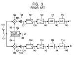
- a conventional direct conversion circuit is described with reference to Fig. 3.
- a reception signal 131 received by an antenna 101 is input to mixers 103 and 104.
- cosine waves 133 and sine waves 134 are output from a phase shifter 102, to which a local oscillation signal 132 (Lo) is input, and are input to the mixers 103 and 104, respectively.
- the mixer 103 outputs a signal 135 by mixing the reception signal 131 and the cosine waves 133 and performing downconversion, while the mixer 104 outputs a signal 136 by mixing the reception signal 131 and the sine waves 134 and performing downconversion.
- the signals 135 and 136 are output as signals 137 and 138, and after unnecessary frequency components are eliminated, the signals 137 and 138 are output as signals 139 and 140.
- the signals 139 and 140 are amplified to predetermined levels by amplifiers 109 and 110, and their output signals 141 and 142 are shaped in waveform by analog root Nyquist filters 111 and 112, whereby a baseband I signal 143 and a baseband Q signal 144 in shaped waveform are obtained.
- the baseband I signal 143 and the baseband Q signal 144 are converted into digital signals by A/D converters 113 and 114, whereby signals 145 and 146 are obtained (see, for example, Japanese Unexamined Patent Application Publication No. 09-168037 (Fig. 3)).
- a direct conversion circuit which includes first and second mixers to which a radio frequency signal is input, an oscillator for supplying the first and second mixers with local oscillation signals whose phases are orthogonal to each other, a baseband processing circuit for processing baseband signals output from the first and second mixers, and a level-difference correcting circuit in a stage before the first and second mixers which, by changing relative levels of the radio frequency signal input to the first mixer and the radio frequency signal input to the second mixer, corrects the two baseband signals input to the baseband processing circuit so that the levels of both are equal to each other.
- a level correcting voltage corresponding to a difference in level between the two baseband signals input to the baseband processing circuit is output from the baseband processing circuit and is input to the level-difference correcting circuit.
- the level-difference correcting circuit may include first and second transistors differential-connected to each other and having bases between which the radio frequency signal is input, third and fourth transistors having emitters connected to the collector of the first transistor, and fifth and sixth transistors having emitters connected to the collector of the second transistor.
- Load resistors may be respectively connected to the collectors of the third to sixth transistors. Radio frequency signals output from the collectors of the first and third transistors may be input to the first mixer, and radio frequency signals output from the collectors of the second and fourth transistor may be input to the second mixer.
- the level correcting voltage may be input between the bases of the third and sixth transistors and may be input between the bases of the fourth and fifth transistors.
- a level-difference correcting circuit which, by changing relative levels of the radio frequency signal input to the first mixer and the radio frequency signal input to the second mixer, corrects the two baseband signals input to the baseband processing circuit so that the levels of both are equal to each other is provided.
- bit errors can be eliminated.
- a level correcting voltage corresponding to a difference in level between the two baseband signals input to the baseband processing circuit is output from the baseband processing circuit, and the level correcting voltage is input to the level-difference correcting circuit.
- the level-difference correcting circuit includes first and second transistors differential-connected and having bases between which the radio frequency signal is input, third and fourth transistors having emitters connected to the collector of the first transistor, and fifth and sixth transistors having emitters connected to the collector of the second transistor, load resistors are respectively connected to the collectors of the third to sixth transistors.
- Radio frequency signals output from the collectors of the first and third transistors are input to the first mixer and radio frequency signals output from the collectors of the second and fourth transistor are input to the second mixer, and the level correcting voltage is input between the bases of the third and sixth transistors and between the bases of the fourth and fifth transistors.
- a radio frequency signal (RF signal) received by an antenna is input to a first mixer 2 and a second mixer 3 through a level correcting circuit 1.
- a local oscillation signal is input from an oscillator 4 to the first and second mixers 2 and 3, with it input to the mixer 3 through a 90-degree phase shifter, so that the inputs have orthogonal phases.
- the frequency of the local oscillation signal is equal to that of the received radio frequency signal.
- baseband signals (I and Q signals) whose phases are orthogonal to each other are output from the first and second mixers 2 and 3.
- the first and second mixers 2 and 3 are formed by a balanced circuit.
- the baseband I signal output from the first mixer 2 is amplified by a baseband amplifier 6 and is input to a baseband processing circuit 8, and also the baseband Q signal output from the second mixer 3 is amplified by a baseband amplifier 7 and is input to the baseband processing circuit 8.
- filters, etc. are provided in stages before and after each of the baseband amplifiers 6 and 7, their representation is omitted.
- the baseband processing circuit 8 includes an A/D conversion unit 8a for converting the baseband I signal into a digital signal, an A/D conversion unit 8b for converting the baseband Q signal into a digital signal, and a subtracting unit 8c for calculating the difference between the two digital signals, whereby the digital signals are processed.
- A/D conversion unit 8a for converting the baseband I signal into a digital signal
- A/D conversion unit 8b for converting the baseband Q signal into a digital signal
- a subtracting unit 8c for calculating the difference between the two digital signals, whereby the digital signals are processed.
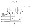
- the level correcting circuit 1 having the above configuration is configured so that the input level correcting voltage can relatively change the level of the radio frequency signal input to the mixer 2 and the level of the radio frequency signal input to the mixer 3. Its specific circuit is shown in Fig. 2.
- the radio frequency signal from the antenna is input between the bases of first and second transistors 11 and 12 which are differential-connected to each other.
- the emitter of the first transistor 11 and the emitter of the second transistor 12 are both connected to a constant current supply 13, whereby differential connection is established.
- the collector of the first transistor 11 connects to the emitters of third and fourth transistors 14 and 15, and their collectors are supplied with power by their load resistors 16 and 17.
- the collector of the second transistor 12 connects to the emitters of fifth and sixth transistors 18 and 19, and their collectors are supplied with power by their load resistors 20 and 21.
- the base of-the third transistor 14 and the base of the sixth transistor 19 are connected to each other, and the base of the fourth transistor 15 and the base of the fifth transistor 18 are connected to each other.
- the level correcting voltage C which is balanced, is input between the bases of the third and sixth transistors 14 and 19 and between the bases of the fourth and fifth transistors 15 and 18.
- a balanced signal generated between the collector (point A) of the third transistor 14 and the collector (point A') of the fifth transistor 18 is input to the first mixer 2 in a balanced manner
- a balanced signal generated between the collector (point B) of the fourth transistor 15 and the collector (point B') of the sixth transistor 19 is input to the second mixer 3 in a balanced manner.
- a radio frequency signal generated between points A and A' and a radio frequency signal generated between points B and B' have equal levels.
- the level of the radio frequency signal generated between points A and A' is greater than the level of the radio frequency signal generated between points B and B'
- the level of the radio frequency signal generated between points A and A' is less than that of the radio frequency signal generated between points B and B'.
- the level of the radio frequency signal input to the first mixer 2 and the level of the radio frequency signal input to the second mixer 3 are relatively changed by the level correcting voltage C.
- the baseband I signal and baseband Q signal input to the baseband processing circuit 8 are controlled to be at the same level.
- bit errors are eliminated in the process of signal processing in the baseband processing circuit 8.
Landscapes
- Engineering & Computer Science (AREA)
- Computer Networks & Wireless Communication (AREA)
- Signal Processing (AREA)
- Power Engineering (AREA)
- Superheterodyne Receivers (AREA)
Abstract
Description
- The present invention relates to a direct conversion circuit for directly outputting a baseband signal from a mixer circuit.
- A conventional direct conversion circuit is described with reference to Fig. 3. A
reception signal 131 received by anantenna 101 is input tomixers cosine waves 133 andsine waves 134 are output from aphase shifter 102, to which a local oscillation signal 132 (Lo) is input, and are input to themixers mixer 103 outputs asignal 135 by mixing thereception signal 131 and thecosine waves 133 and performing downconversion, while themixer 104 outputs asignal 136 by mixing thereception signal 131 and thesine waves 134 and performing downconversion. - Next, after direct-current offsets are eliminated by
AC couplings signals signals signals signals signals amplifiers output signals filters baseband I signal 143 and abaseband Q signal 144 in shaped waveform are obtained. The baseband I signal 143 and thebaseband Q signal 144 are converted into digital signals by A/D converters signals - In the above-described conventional configuration, even if there is no level difference between the reception signals input to one
mixer 103 and theother mixer 104, for example, when there is a difference in conversion gain between themixer 103 and theother mixer 104, and similarly, when there is a difference in gain between oneamplifier 109 and theother amplifier 110, a level difference occurs between the baseband I signal input to the A/D converter 113 and the baseband Q signal input to the A/D converter 114. In this state, conversion of each baseband signal into a digital signal by each A/D converter causes bit errors. - It is an object of the present invention to reduce bit errors by equalizing the levels of two baseband signals which are input to a baseband processing circuit.
- According to an aspect of the present invention, a direct conversion circuit is provided which includes first and second mixers to which a radio frequency signal is input, an oscillator for supplying the first and second mixers with local oscillation signals whose phases are orthogonal to each other, a baseband processing circuit for processing baseband signals output from the first and second mixers, and a level-difference correcting circuit in a stage before the first and second mixers which, by changing relative levels of the radio frequency signal input to the first mixer and the radio frequency signal input to the second mixer, corrects the two baseband signals input to the baseband processing circuit so that the levels of both are equal to each other.
- Preferably, a level correcting voltage corresponding to a difference in level between the two baseband signals input to the baseband processing circuit is output from the baseband processing circuit and is input to the level-difference correcting circuit.
- The level-difference correcting circuit may include first and second transistors differential-connected to each other and having bases between which the radio frequency signal is input, third and fourth transistors having emitters connected to the collector of the first transistor, and fifth and sixth transistors having emitters connected to the collector of the second transistor. Load resistors may be respectively connected to the collectors of the third to sixth transistors. Radio frequency signals output from the collectors of the first and third transistors may be input to the first mixer, and radio frequency signals output from the collectors of the second and fourth transistor may be input to the second mixer. The level correcting voltage may be input between the bases of the third and sixth transistors and may be input between the bases of the fourth and fifth transistors.
- As described above, according to the present invention, in a stage before first and second mixers, a level-difference correcting circuit which, by changing relative levels of the radio frequency signal input to the first mixer and the radio frequency signal input to the second mixer, corrects the two baseband signals input to the baseband processing circuit so that the levels of both are equal to each other is provided. Thus, bit errors can be eliminated.
- Also, a level correcting voltage corresponding to a difference in level between the two baseband signals input to the baseband processing circuit is output from the baseband processing circuit, and the level correcting voltage is input to the level-difference correcting circuit. Thus, even if there is a level difference between the two baseband signals input to the baseband processing circuit, automatic correction so that both signals are in the same level is performed, whereby bit errors are eliminated.
- Also, the level-difference correcting circuit includes first and second transistors differential-connected and having bases between which the radio frequency signal is input, third and fourth transistors having emitters connected to the collector of the first transistor, and fifth and sixth transistors having emitters connected to the collector of the second transistor, load resistors are respectively connected to the collectors of the third to sixth transistors. Radio frequency signals output from the collectors of the first and third transistors are input to the first mixer and radio frequency signals output from the collectors of the second and fourth transistor are input to the second mixer, and the level correcting voltage is input between the bases of the third and sixth transistors and between the bases of the fourth and fifth transistors. Thus, relative levels of the radio frequency signal input to the first mixer and the radio frequency signal input to the second mixer can be changed.
-
- Fig. 1 is a circuit diagram showing a direct conversion circuit of the present invention,
- Fig. 2 is a specific circuit diagram of a level correcting circuit for use in a direct conversion circuit of the present invention, and
- Fig. 3 is a circuit diagram showing the configuration of a conventional direct conversion circuit.
- A direct conversion circuit of the present invention is described with reference to Figs. 1 and 2. At first, in Fig. 1, a radio frequency signal (RF signal) received by an antenna (not shown) is input to a first mixer 2 and a
second mixer 3 through a level correcting circuit 1. A local oscillation signal is input from an oscillator 4 to the first andsecond mixers 2 and 3, with it input to themixer 3 through a 90-degree phase shifter, so that the inputs have orthogonal phases. The frequency of the local oscillation signal is equal to that of the received radio frequency signal. Thus, baseband signals (I and Q signals) whose phases are orthogonal to each other are output from the first andsecond mixers 2 and 3. The first andsecond mixers 2 and 3 are formed by a balanced circuit. - The baseband I signal output from the first mixer 2 is amplified by a
baseband amplifier 6 and is input to abaseband processing circuit 8, and also the baseband Q signal output from thesecond mixer 3 is amplified by abaseband amplifier 7 and is input to thebaseband processing circuit 8. Although filters, etc., are provided in stages before and after each of thebaseband amplifiers - The
baseband processing circuit 8 includes an A/D conversion unit 8a for converting the baseband I signal into a digital signal, an A/D conversion unit 8b for converting the baseband Q signal into a digital signal, and asubtracting unit 8c for calculating the difference between the two digital signals, whereby the digital signals are processed. When there is a level difference between the baseband I signal and the baseband Q signal which are respectively input to the A/D conversion units baseband processing circuit 8 outputs a level correcting voltage C corresponding to the level difference of each input baseband signal. The level correcting voltage C is fed back to the level correcting circuit 1. - The level correcting circuit 1 having the above configuration is configured so that the input level correcting voltage can relatively change the level of the radio frequency signal input to the mixer 2 and the level of the radio frequency signal input to the
mixer 3. Its specific circuit is shown in Fig. 2. - In Fig. 2, the radio frequency signal from the antenna is input between the bases of first and
second transistors first transistor 11 and the emitter of thesecond transistor 12 are both connected to a constantcurrent supply 13, whereby differential connection is established. The collector of thefirst transistor 11 connects to the emitters of third andfourth transistors load resistors second transistor 12 connects to the emitters of fifth andsixth transistors load resistors - The base of-the
third transistor 14 and the base of thesixth transistor 19 are connected to each other, and the base of thefourth transistor 15 and the base of thefifth transistor 18 are connected to each other. The level correcting voltage C, which is balanced, is input between the bases of the third andsixth transistors fifth transistors third transistor 14 and the collector (point A') of thefifth transistor 18 is input to the first mixer 2 in a balanced manner, and a balanced signal generated between the collector (point B) of thefourth transistor 15 and the collector (point B') of thesixth transistor 19 is input to thesecond mixer 3 in a balanced manner. - Here, when the level correcting voltage C is zero, that is, the bases of the third and
sixth transistors fifth transistors sixth transistors fifth transistors sixth transistors fifth transistors second mixer 3 are relatively changed by the level correcting voltage C. - As a result, the baseband I signal and baseband Q signal input to the
baseband processing circuit 8 are controlled to be at the same level. Thus, bit errors are eliminated in the process of signal processing in thebaseband processing circuit 8.
Claims (3)
- A direct conversion circuit comprising:first and second mixers to which a radio frequency signal is input;an oscillator for supplying the first and second mixers with local oscillation signals whose phases are orthogonal to each other;a baseband processing circuit for processing baseband signals output from the first and second mixers; anda level-difference correcting circuit in a stage before the first and second mixers, the level-difference correcting circuit correcting, by changing relative levels of the radio frequency signal input to the first mixer and the radio frequency signal input to the second mixer, the two baseband signals input to the baseband processing circuit so that the levels of both are equal to each other.
- A direct conversion circuit according to claim 1, wherein a level correcting voltage corresponding to a difference in level between the two baseband signals input to the baseband processing circuit is output from the baseband processing circuit and is input to the level-difference correcting circuit.
- A direct conversion circuit according to claim 1 or 2, wherein:the level-difference correcting circuit includes:first and second transistors differential-connected to each other and having bases between which the radio frequency signal is input;third and fourth transistors having emitters connected to the collector of the first transistor, andfifth and sixth transistors having emitters connected to the collector of the second transistor;load resistors are respectively connected to the collectors of the third to sixth transistors;radio frequency signals output from the collectors of the first and third transistors are input to the first mixer and radio frequency signals output from the collectors of the second and fourth transistors are input to the second mixer; andthe level correcting voltage is input between the bases of the third and sixth transistors and is input between the bases of the fourth and fifth transistors.
Applications Claiming Priority (2)
| Application Number | Priority Date | Filing Date | Title |
|---|---|---|---|
| JP2003076939 | 2003-03-20 | ||
| JP2003076939A JP2004289338A (en) | 2003-03-20 | 2003-03-20 | Direct conversion circuit |
Publications (2)
| Publication Number | Publication Date |
|---|---|
| EP1460770A2 true EP1460770A2 (en) | 2004-09-22 |
| EP1460770A3 EP1460770A3 (en) | 2008-09-17 |
Family
ID=32821369
Family Applications (1)
| Application Number | Title | Priority Date | Filing Date |
|---|---|---|---|
| EP04003498A Withdrawn EP1460770A3 (en) | 2003-03-20 | 2004-02-17 | Direct conversion circuit having reduced bit errors |
Country Status (3)
| Country | Link |
|---|---|
| US (1) | US7209723B2 (en) |
| EP (1) | EP1460770A3 (en) |
| JP (1) | JP2004289338A (en) |
Cited By (1)
| Publication number | Priority date | Publication date | Assignee | Title |
|---|---|---|---|---|
| CN119448940A (en) * | 2025-01-09 | 2025-02-14 | 龙骧鑫睿(厦门)科技有限公司 | A mixer circuit |
Families Citing this family (2)
| Publication number | Priority date | Publication date | Assignee | Title |
|---|---|---|---|---|
| KR101223207B1 (en) | 2010-10-28 | 2013-01-17 | 광주과학기술원 | Tracker node, peer node and method for multi-swam collaboration in bittorrent network |
| US9231713B2 (en) * | 2014-03-07 | 2016-01-05 | Charlie Chen | Method for designing an analog Nyquist filter |
Family Cites Families (10)
| Publication number | Priority date | Publication date | Assignee | Title |
|---|---|---|---|---|
| US4866395A (en) * | 1988-11-14 | 1989-09-12 | Gte Government Systems Corporation | Universal carrier recovery and data detection for digital communication systems |
| JPH09168037A (en) | 1995-12-15 | 1997-06-24 | Matsushita Electric Ind Co Ltd | Direct conversion receiver |
| US5878089A (en) * | 1997-02-21 | 1999-03-02 | Usa Digital Radio Partners, L.P. | Coherent signal detector for AM-compatible digital audio broadcast waveform recovery |
| US6356736B2 (en) * | 1997-02-28 | 2002-03-12 | Maxim Integrated Products, Inc. | Direct-conversion tuner integrated circuit for direct broadcast satellite television |
| US6118322A (en) * | 1998-11-03 | 2000-09-12 | Motorola, Inc. | Method and apparatus for reducing even order distortion in differential circuits |
| US6314278B1 (en) * | 1998-12-30 | 2001-11-06 | Uniden America Corporation | Adjusting gain in a receiver using received signal sample values |
| US6714776B1 (en) * | 1999-09-28 | 2004-03-30 | Microtune (Texas), L.P. | System and method for an image rejecting single conversion tuner with phase error correction |
| US20030003891A1 (en) * | 2001-07-02 | 2003-01-02 | Nokia Corporation | Method to improve I/Q-amplitude balance and receiver quadrature channel performance |
| JP2003273947A (en) | 2002-03-13 | 2003-09-26 | Hitachi Kokusai Electric Inc | Direct conversion receiver |
| TW200518486A (en) * | 2002-11-15 | 2005-06-01 | Interdigital Tech Corp | Compensating for analog radio component impairments to relax specifications |
-
2003
- 2003-03-20 JP JP2003076939A patent/JP2004289338A/en active Pending
-
2004
- 2004-02-17 EP EP04003498A patent/EP1460770A3/en not_active Withdrawn
- 2004-03-16 US US10/801,370 patent/US7209723B2/en not_active Expired - Fee Related
Cited By (1)
| Publication number | Priority date | Publication date | Assignee | Title |
|---|---|---|---|---|
| CN119448940A (en) * | 2025-01-09 | 2025-02-14 | 龙骧鑫睿(厦门)科技有限公司 | A mixer circuit |
Also Published As
| Publication number | Publication date |
|---|---|
| US20040185812A1 (en) | 2004-09-23 |
| US7209723B2 (en) | 2007-04-24 |
| EP1460770A3 (en) | 2008-09-17 |
| JP2004289338A (en) | 2004-10-14 |
Similar Documents
| Publication | Publication Date | Title |
|---|---|---|
| US6370372B1 (en) | Subharmonic mixer circuit and method | |
| US6999746B2 (en) | Image rejection mixer | |
| US7196579B2 (en) | Gain-controlled amplifier, receiver circuit and radio communication device | |
| US6763227B2 (en) | Systems and methods for modulator calibration | |
| US4470147A (en) | Radio receiver with quadrature demodulation and digital processing | |
| US9490858B2 (en) | Transmitter capable of reducing local oscillation leakage and in-phase/quadrature-phase (I/Q) mismatch and adjusting methods thereof | |
| US20030003891A1 (en) | Method to improve I/Q-amplitude balance and receiver quadrature channel performance | |
| US7949313B2 (en) | Direct conversion device with compensation means for a transmission path of a wireless communication equipment | |
| JP4429161B2 (en) | Mirror suppression circuit and receiver using such a circuit | |
| US20040174199A1 (en) | Multiplier circuit | |
| US6492914B2 (en) | Filter-provided device | |
| CN101540640A (en) | Carrier leak correcting circuit used at front end of emission and method thereof | |
| US7209723B2 (en) | Direct conversion circuit having reduced bit errors | |
| US6927629B2 (en) | Differential amplifier having improved balanced and linearity | |
| US6320529B1 (en) | A/D conversion apparatus and a radio apparatus | |
| US20050157819A1 (en) | Receivers gain imbalance calibration circuits and methods thereof | |
| JP6408291B2 (en) | IQ mismatch correction method and transmitter / receiver | |
| US6792254B1 (en) | Method of comparing the amplitudes of two electric signals | |
| JP5292061B2 (en) | Quadrature demodulator | |
| EP1022848B1 (en) | Amplifier and radio communication apparatus using the same | |
| US20130223569A1 (en) | Wireless receiver | |
| US7443220B2 (en) | Phase shift circuit and phase correcting method | |
| CN201717850U (en) | Carrier leakage correction circuit | |
| JP2010056605A (en) | Mixer circuit, method for manufacturing the same, and semiconductor integrated circuit | |
| JP3392679B2 (en) | Frequency converter and radio receiver using the same |
Legal Events
| Date | Code | Title | Description |
|---|---|---|---|
| PUAI | Public reference made under article 153(3) epc to a published international application that has entered the european phase |
Free format text: ORIGINAL CODE: 0009012 |
|
| AK | Designated contracting states |
Kind code of ref document: A2 Designated state(s): AT BE BG CH CY CZ DE DK EE ES FI FR GB GR HU IE IT LI LU MC NL PT RO SE SI SK TR |
|
| AX | Request for extension of the european patent |
Extension state: AL LT LV MK |
|
| PUAL | Search report despatched |
Free format text: ORIGINAL CODE: 0009013 |
|
| AK | Designated contracting states |
Kind code of ref document: A3 Designated state(s): AT BE BG CH CY CZ DE DK EE ES FI FR GB GR HU IE IT LI LU MC NL PT RO SE SI SK TR |
|
| AX | Request for extension of the european patent |
Extension state: AL LT LV MK |
|
| 17P | Request for examination filed |
Effective date: 20090311 |
|
| AKX | Designation fees paid |
Designated state(s): DE FR GB |
|
| STAA | Information on the status of an ep patent application or granted ep patent |
Free format text: STATUS: THE APPLICATION HAS BEEN WITHDRAWN |
|
| 18W | Application withdrawn |
Effective date: 20090821 |