EP1460696A2 - A high absorption donor substrate coatable with organic layer(s) transferable in response to incident laser light - Google Patents
A high absorption donor substrate coatable with organic layer(s) transferable in response to incident laser light Download PDFInfo
- Publication number
- EP1460696A2 EP1460696A2 EP04075748A EP04075748A EP1460696A2 EP 1460696 A2 EP1460696 A2 EP 1460696A2 EP 04075748 A EP04075748 A EP 04075748A EP 04075748 A EP04075748 A EP 04075748A EP 1460696 A2 EP1460696 A2 EP 1460696A2
- Authority
- EP
- European Patent Office
- Prior art keywords
- donor
- reflection layer
- absorber
- metallic heat
- reflectivity
- Prior art date
- Legal status (The legal status is an assumption and is not a legal conclusion. Google has not performed a legal analysis and makes no representation as to the accuracy of the status listed.)
- Granted
Links
Images


Classifications
-
- B—PERFORMING OPERATIONS; TRANSPORTING
- B41—PRINTING; LINING MACHINES; TYPEWRITERS; STAMPS
- B41M—PRINTING, DUPLICATING, MARKING, OR COPYING PROCESSES; COLOUR PRINTING
- B41M5/00—Duplicating or marking methods; Sheet materials for use therein
- B41M5/26—Thermography ; Marking by high energetic means, e.g. laser otherwise than by burning, and characterised by the material used
- B41M5/40—Thermography ; Marking by high energetic means, e.g. laser otherwise than by burning, and characterised by the material used characterised by the base backcoat, intermediate, or covering layers, e.g. for thermal transfer dye-donor or dye-receiver sheets; Heat, radiation filtering or absorbing means or layers; combined with other image registration layers or compositions; Special originals for reproduction by thermography
- B41M5/42—Intermediate, backcoat, or covering layers
-
- B—PERFORMING OPERATIONS; TRANSPORTING
- B60—VEHICLES IN GENERAL
- B60N—SEATS SPECIALLY ADAPTED FOR VEHICLES; VEHICLE PASSENGER ACCOMMODATION NOT OTHERWISE PROVIDED FOR
- B60N2/00—Seats specially adapted for vehicles; Arrangement or mounting of seats in vehicles
- B60N2/58—Seat coverings
- B60N2/60—Removable protective coverings
- B60N2/6018—Removable protective coverings attachments thereof
- B60N2/6027—Removable protective coverings attachments thereof by hooks, staples, clips, snap fasteners or the like
-
- B—PERFORMING OPERATIONS; TRANSPORTING
- B41—PRINTING; LINING MACHINES; TYPEWRITERS; STAMPS
- B41M—PRINTING, DUPLICATING, MARKING, OR COPYING PROCESSES; COLOUR PRINTING
- B41M5/00—Duplicating or marking methods; Sheet materials for use therein
- B41M5/26—Thermography ; Marking by high energetic means, e.g. laser otherwise than by burning, and characterised by the material used
- B41M5/40—Thermography ; Marking by high energetic means, e.g. laser otherwise than by burning, and characterised by the material used characterised by the base backcoat, intermediate, or covering layers, e.g. for thermal transfer dye-donor or dye-receiver sheets; Heat, radiation filtering or absorbing means or layers; combined with other image registration layers or compositions; Special originals for reproduction by thermography
- B41M5/41—Base layers supports or substrates
-
- H—ELECTRICITY
- H10—SEMICONDUCTOR DEVICES; ELECTRIC SOLID-STATE DEVICES NOT OTHERWISE PROVIDED FOR
- H10K—ORGANIC ELECTRIC SOLID-STATE DEVICES
- H10K71/00—Manufacture or treatment specially adapted for the organic devices covered by this subclass
- H10K71/10—Deposition of organic active material
- H10K71/18—Deposition of organic active material using non-liquid printing techniques, e.g. thermal transfer printing from a donor sheet
-
- B—PERFORMING OPERATIONS; TRANSPORTING
- B41—PRINTING; LINING MACHINES; TYPEWRITERS; STAMPS
- B41M—PRINTING, DUPLICATING, MARKING, OR COPYING PROCESSES; COLOUR PRINTING
- B41M5/00—Duplicating or marking methods; Sheet materials for use therein
- B41M5/26—Thermography ; Marking by high energetic means, e.g. laser otherwise than by burning, and characterised by the material used
- B41M5/40—Thermography ; Marking by high energetic means, e.g. laser otherwise than by burning, and characterised by the material used characterised by the base backcoat, intermediate, or covering layers, e.g. for thermal transfer dye-donor or dye-receiver sheets; Heat, radiation filtering or absorbing means or layers; combined with other image registration layers or compositions; Special originals for reproduction by thermography
- B41M5/42—Intermediate, backcoat, or covering layers
- B41M5/426—Intermediate, backcoat, or covering layers characterised by inorganic compounds, e.g. metals, metal salts, metal complexes
-
- H—ELECTRICITY
- H10—SEMICONDUCTOR DEVICES; ELECTRIC SOLID-STATE DEVICES NOT OTHERWISE PROVIDED FOR
- H10K—ORGANIC ELECTRIC SOLID-STATE DEVICES
- H10K71/00—Manufacture or treatment specially adapted for the organic devices covered by this subclass
Definitions
- the present invention relates to thermal transfer of organic materials from a donor element to a receiving device, such as an OLED device.
- organic electroluminescent (EL) displays also known as organic light-emitting diode devices, or OLED devices
- OLED devices organic light-emitting diode devices
- RGB pixels red, green, and blue color pixels
- the basic OLED device has in common an anode, a cathode, and an organic EL medium sandwiched between the anode and the cathode.
- the organic EL medium can consist of one or more layers of organic thin films, where one of the layers is primarily responsible for light generation or electroluminescence. This particular layer is generally referred to as the emissive layer of the organic EL medium.
- organic layers present in the organic EL medium can provide electronic transport functions primarily and are referred to as either the hole transport layer (for hole transport) or electron transport layer (for electron transport).
- hole transport layer for hole transport
- electron transport layer for electron transport
- a suitable method for patterning high-resolution OLED displays has been disclosed in commonly-assigned US-A-5,851,709 by Grande and others this method is comprised of the following sequences of steps: 1) providing a substrate having opposing first and second surfaces; 2) forming a light-transmissive heat-insulating layer over the first surface of the substrate; 3) forming a light-absorbing layer over the heat-insulating layer; 4) providing the substrate with an array of openings extending from the second surface to the heat-insulating layer; 5) providing a transferable color-forming organic donor layer formed on the light-absorbing layer; 6) precision aligning the donor substrate with the display substrate in an oriented relationship between the openings in the substrate and the corresponding color pixels on the device; and 7) employing a source of radiation for producing sufficient heat at the light-absorbing layer over the openings to cause the transfer of the organic layer on the donor substrate to the display substrate.
- a problem with the Grande and others approach is that patterning of an array of openings on the donor substrate is required. Another problem is that
- Littman and Tang teach the patternwise transfer of organic EL material from an unpatterned donor sheet to an EL substrate.
- a series of patents by Wolk and others (US-A-6,114,088; US-A-6,140,009; US-A-6,214,520; and US-A-6,221,553) teaches a method that can transfer the luminescent layer of an EL device from a donor element to a substrate by heating selected portions of the donor with a laser beam. Each layer is an operational or non-operational layer that is utilized in the function of the device.
- a donor containing the electroluminescent materials is heated by radiation and transferred to a receiver which may already contain a portion of the active device.
- the device may then be finished by the application of further layers.
- This process allows the patterning of colors by the use of a suitable donor which contains an electron or hole conductors host and a dopant.
- the final light emitting device must have the dopant mixed together to give a good emission. It is difficult to co-evaporate two or more materials simultaneously and maintain a constant controlled ratio. The resulting emission from these radiation-transferred devices also have need for improved efficiency.
- Deboer and Spahn (commonly-assigned US-A-5,244,770) teaches a donor element for color transfer in the field of color printing. They introduce the concept of an anti-reflection layer located between a transparent support, and a heat absorbing metal layer. This element is used to transfer a dye layer comprising a binder and a sublimable dye.
- a binder is common in the field of color printing, but is inappropriate in the fabrication of OLED devices. It is difficult to transfer an organic material without contamination from the binder. In a color print, low levels of contamination can be tolerated, but such contamination would be unacceptable in an electroluminescent device such as an OLED, compromising lifetime, efficiency, and appearance.
- This object is achieved in a method of making a high absorption donor substrate which can be coated with one or more organic material layers and for use in providing one or more OLED materials to an OLED device in response to laser light substantially within a predetermined wavelength range, includes:
- a tuned high absorption donor substrate for laser-thermal-transfer can have a high efficiency absorber which can absorb 95% to 100% of the light striking it. This improves optical efficiency of a donor element by a factor of two over simple donor substrates for laser-thermal-transfer with a simple metallic heat-absorbing layer as the absorber, and thus provides greater transfer efficiency at a given light intensity.
- the very low reflectivity absorber greatly reduces the variability in the absorption efficiency of the donor substrate, and allows a uniform transfer of organic material from a donor element made from the donor substrate even when operating near the transfer threshold. OLED materials are known to be sensitive to excessive heating, so the best transfer conditions are expected to be near the transfer threshold for a wide variety of systems.
- a donor with an average reflectivity of greater than only 10% can have a variability in the transfer threshold of up to 18%. Furthermore, since contamination is critical in electroluminescent devices such as an OLED, it is advantageous to perform transfers for OLED devices with an organic layer which is transferred in its entirety, as opposed to an organic layer with an inert binder which is either partially transferred or not transferred at all.
- the simple donor substrate 12 shown in FIG. 1 suffers from both poor efficiency and poor uniformity.
- the poor efficiency is a result of the intrinsic reflectivity of most metals. Typical metal reflectivities are on the order of 50% to 98%. Since reflected light cannot contribute to the heating of the metallic heat-absorbing layer 24, one must compensate by supplying an abundance of laser power.
- each layer in the element can be characterized by a thickness (t) and a refractive index (n).
- the refractive index is a real number.
- incident laser light 30 first encounters the non-transfer surface 36 of the transparent support 20. A portion of the incident laser light 30 is reflected 32 from the non-transfer surface. Another portion of the incident laser light 30 enters the transparent support element, and encounters the metallic heat-absorbing layer 22. If the metallic heat-absorbing layer 22 is sufficiently thick (typically greater than 200 nm) an insignificant fraction of the light is transmitted (not shown). A portion of the incident laser light 30 which encounters the metallic heat-absorbing layer 22 is absorbed by that layer, and converted to heat. Another portion of the laser light reflected back toward the non-transfer surface of the simple donor substrate 12. The reflected laser light 34 leaving the simple donor substrate 12 occupies the same space as the reflected laser light 32, and combines with it. If the two reflected laser lights are coherent, as is usually the case for laser light, the amplitudes of the electric fields will add, causing combined magnitude of the two reflected laser lights to depend on their relative phases.
- the phase of the reflected laser light 34 differs from the phase of the reflected laser light 32 based on the distance it has traveled through the transparent support element 20. There is an additional phase shift incurred when reflected laser light 34 reflects from the metallic heat-absorbing layer 22. The consequence of this behavior is that the combined magnitude of the two reflected laser lights depends on the precise thickness of the transparent support element 20. If no significant portion of the laser light is transmitted, than variations in the energy reflected must be complemented by variations in the energy absorbed in the metallic heat-absorbing layer 22. Since the thickness of the transparent support element 20 cannot generally be controlled to the degree required, this variation is a major source of poor uniformity of the absorption by the simple donor substrate 12.
- FIG. 2 depicts the absorption curve which is the result of applying the methodology in Fowles to the optical system in Example 1.
- the absorption peak 40 occurs whenever the thickness of the transparent support element 20 is such that the relative phases of the two reflected lights in an odd multiple of pi (out of phase)
- the absorption valley 42 occurs whenever the thickness of the transparent support element 20 is such that the relative phases of the two reflected lights is an even multiple of pi (in phase).
- the absorption level of the simple donor substrate 12 at the absorption peak will be denoted as A peak
- the absorption level of the simple donor substrate 12 at the absorption valley 42 will be denoted as A valley . From the absorption curve in FIG. 2, one can see that a variation of only 0.1 micrometer in the substrate thickness will cause the full absorption variation, and no reasonably priced substrate will be held to these tolerances. This means that this effect represents an uncontrolled variation in the absorption of the simple donor substrate 12.
- MAV micro absorption variation
- FIG. 3 is a representation of a photograph taken of a simple donor substrate as depicted in FIG. 1.
- the simple donor substrate 12 was chromium coating on a 75 micrometer thick Kapton® support.
- the lighting was a from a light box with two uncoated fluorescent bulbs, a white plastic diffuser plate, and a green plastic filter, which provides a diffuse green illumination with a wavelength which was measured to be 548 nm and a bandwidth which was measured to be 8 nm.
- the light and dark fringes in FIG. 3 correspond to the peaks and valleys in the graph of FIG. 2, as the thickness of the Kapton® varies across its surface. The fringes varied from about 1 to 5 mm in separation.
- This optical arrangement is slightly different than the one which would occur in laser writing, but the fringe effect is similar.
- a minimum of light is reflected (dark fringe)
- a maximum of light is absorbed, and the simple donor substrate 12 would have enhanced sensitivity.
- a maximum of light is reflected (bright fringe)
- a minimum of light is absorbed, and the simple donor substrate 12 would have reduced sensitivity.
- This variation would be desirable for the purpose of laser thermal transfer using a simple donor substrate 12.
- the overall behavior of the optical system depicted in FIG. 1 is determined by the interference of reflected laser light 32 and reflected laser light 34, as seen in FIG. 3, one can calculate the magnitude of each of these reflected lights independently as if there were no interference.
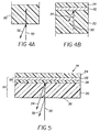
- FIG. 4A if one eliminates reflected laser light 34 by assuming that there is no metallic absorbing layer 22, and that the transparent support element 20 is semi-infinite in extent, one can compute a quantity equal to the magnitude of reflected laser light 34 divided by the incident laser light 30, which will be referred to as the "donor back surface reflectivity".
- the incident laser light 30 which will be referred to as the "donor back surface reflectivity".
- the intensity of the reflected laser light 34 divided by the intensity of the incident laser light 30 will be referred to as the "donor absorber reflectivity”.
- the fraction of incident laser light 30 absorbed by the donor absorber will be referred to as the "donor absorber efficiency”.
- the reduction of the donor back surface reflectivity can be accomplished by applying an anti-reflection coating onto the non-transfer side of the donor substrate. This will be referred to as a back surface anti-reflection layer.
- This well known solution can be accomplished by coating a single quarter wavelength layer of a low refractive index material onto the non transfer side of the donor substrate.
- a single layer back surface anti-reflection coating is not fully effective. It is well known that an ideal single layer anti-reflection coating applied to a dielectric must have a refractive index equal in value to the square root of the refractive index of the dielectric.
- Typical values of the refractive index of the transparent support element, n s range from 1.4 to 1.75, requiring that the refractive index for the donor back surface anti-reflection layer to be the appropriate value between 1.18 and 1.32.
- the best low index material for this purpose is known in the art to be MgF 2 with a refractive index of 1.37, which cannot be a perfect match for any of the typical supports, and therefore results in a non-ideal anti-reflection layer.
- Example 2 (prior art; computational): A structure identical to the one proposed in Example 1 has a quarter wavelength layer of MgF2 (148 nm) applied to the non-transfer surface 36 depicted in FIG. 1. One calculates that the donor back surface reflectivity is reduced from 4.0% to 1.25%. As a result, A peak is 58.7%, A valley is 42.5%, and the MAV is reduced from 28.2% to 15.5%. The effectiveness of this approach would improve as n s increases toward the ideal value of 1.88. One could reduce the MAV to zero by using a two layer anti-reflection coating on the non-transfer side of the simple donor substrate 12.
- a better solution for reducing the MAV is to reduce or eliminate the donor absorber reflectivity.
- This can be accomplished by using the formulation shown in FIG. 5.
- a high absorption donor element 14, and more specifically a high absorption donor substrate 16 is fabricated by including an anti-reflection layer between the transparent support element 20 and the metallic heat-absorbing layer 22.
- the anti-reflection layer in this location will be referred to as the absorber anti-reflection layer 28.
- the combination of the metallic heat-absorbing layer 22 and the absorber anti-reflection layer 28 will be referred to as the high efficiency absorber 18. If the material for the absorber anti-reflection layer 28 is properly selected, it will eliminate or greatly reduce the donor absorber reflectivity.
- Example 3 (present invention; computational): A high absorption donor substrate 16 according to FIG. 5 was modeled.
- the transparent support element 20 was selected to be polycarbonate.
- the absorber anti-reflection layer 28 was selected to be amorphous silicon, as one might obtain from sputtering or e-beam evaporation, and the metallic heat-absorbing layer 22 was optically thick chromium (200 nm thick), also as one might obtain from sputtering or e-beam evaporation.
- the optical constants used were the published values, typical of bulk materials (Palik and references therein).
- n s 1.58 (polycarbonate, typical value)
- n a 3.89 (amorphous silicon, Palik)
- k a 0.15 ( amorphous silicon, Palik)
- n m 4.18 (chromium, Palik)
- the donor back surface reflectivity was 5.1 %, and the donor absorber reflectivity was virtually zero (0.003%).
- a peak was 94.99% and A valley of 94.90% resulting in MAV equal to 0.05%.
- Example 1 The performance of Examples 1, 2 and 3 are summarized in Table 1. Of particular note is the low MAV for the high efficiency formulation, indicating a spatially uniform donor absorption level, and the high donor substrate efficiency, indicating a reduction in the amount of laser energy to effect a 100% transfer of organic material. The high efficiency formulation is clearly superior. Table 1 Ex. # Formulation Donor Back Surface Reflectivity Donor Absorber Efficiency MAV Donor Substrate Efficiency 1 simple 4% 50.1% 28.2% 36.1% 2 simple with back surface anti-reflection layer 1.25% 50.9% 15.5% 42.5% 3 high efficiency 5.1% 100% 0.003% 94.9%
- the published values of the optical constants for thin films are often measured from bulk materials.
- the actual optical constants for thin films can be dependant on the conditions under which they are prepared, and often vary somewhat from the published values. For this reason, it is convenient to tune the anti-reflection layer thickness empirically.
- This methodology does not provide an independent measure of the actual film thickness, nor the actual optical constants of the coated layers. These could be obtained by profilometry and ellipsometry respectively, but to fabricate a practical device, one can use published optical values, and computer modeling to predict the performance of a tuned system, and then one fabricates that system by adjusting the thickness of the absorber anti-reflection layer empirically to achieve optimum system performance which will approximate the performance predicted by the model. Small discrepancies are attributed to differences between the actual and bulk optical constants.
- Example 4 (present invention; experimental): Referring to FIG. 5, a high absorption donor substrate 16 was fabricated by applying a nearly ideal index matched absorber anti-reflection layer 28 onto a transparent support element 20.
- the transparent support element 20 was 1.2 mm thick polycarbonate.
- the absorber anti-reflection layer 28 was 99.999% silicon with boron doped to a resistivity of 0.020 ohm-cm and was dc-sputtered in 6 mTorr of argon gas. The boron was included to reduce charging during the dc sputtering process, and is not believed to affect the optical properties of the silicon.
- a series of samples were prepared varying the thickness of the silicon layer in the range of 0 nm and 45 nm.
- the discrepancy could be the inaccuracy of the experimental thickness measurement, or, more likely, the difference between the bulk values for the optical constants reported in the literature, and the actual values obtained by sputtering.
- the best tuned high absorption donor substrate 16 had a measured reflectivity at 800 nm of 5.3%.
- the exposed sample area in the Cary 2500 spectrophotometer is a circle about 15 mm in diameter. Referring to the image in FIG. 3, one is measuring a reflectivity average over many fringes, so the measured values are average reflectivities.
- Example 5 (experimental): The best coatings applied in Example 4 (45 nm Si and 60 nm Cr), were applied to the surface of a 75 micrometer thick UDEL® support.
- the UDEL support is reported by the supplier to have an index of refraction of 1.633 which results in a donor back surface reflectivity of 5.8%.
- the measured reflectivity of the high absorption donor substrate on the Cary 2500 at 800 nm was 5.7%.
- Example 6 (present invention; experimental): A high absorption donor substrate 16 was fabricated in the manner of Example 5, except that the chromium layer was coated to only 40 nm thickness. A layer of 20 nm of 2-tert-butyl-9,10-bis(2-naphthyl)anthracene (TBADN) was vacuum deposited onto the chromium layer, followed by a second layer of 0.25 nm of tetra-tert-butyl-perylene (TBP) to create a blue high absorption donor element 14 for an OLED process. These materials were transferred from the blue high absorption donor element 14 to an in-process OLED device using a scanning infrared laser of 810 nm wavelength to heat the blue high absorption donor element 14.
- TAADN 2-tert-butyl-9,10-bis(2-naphthyl)anthracene
- TBP tetra-tert-butyl-perylene
- the laser spot was 0.010 mm by 2.56 mm, and had a total output power of 1.5 W. It was swept at a rate of 140 mm/s in the direction of the 0.01 mm dimension, thereby exposing the donor element to 4.2 mJ/mm 2 of energy in a time period of approximately 70 microseconds. This exposure was sufficient to transfer the organics from the donor sheet to the in process OLED device. Completion of the device produced a blue color element as would be expected for this chemical combination.
- Example 7 (present invention; experimental): A simple donor element 10 was coated in the manner of Example 6, except that the silicon layer which served as the absorber anti-reflection layer 28 was omitted, creating a blue simple donor element 10 for an OLED process. These materials were transferred from the blue simple donor element 10 to an in-process OLED device using a scanning infrared laser of 810 nm wavelength to heat the blue simple donor element 10. The laser spot was spot was 0.010 mm by 2.56 mm, and had a total output power of 3.0 W. It was swept at a rate of 220 mm/s. This exposure (5.3 mJ/mm 2 in a time period of 45 microseconds) was not sufficient to transfer any the organics from the donor sheet to the in process OLED device.
- Completion of the device produced a green color element as would be expected for an undoped OLED device.
- the same simple blue donor element 10 was employed at a lower sweep rate of 140 mm/s in the direction of the 10 micrometer dimension, thereby exposing the donor element to 8.4 mJ/mm 2 of energy in a time period of 70 microseconds. This exposure was sufficient to transfer the organics from the donor sheet to the in process OLED device.
- Completion of the device produced a blue color element as would be expected for this chemical combination.
- the simple donor element 10 of this example required nearly twice the energy density to accomplish the same transfer as the high absorption donor element 14 in Example 6.
- FIG. 7 shows a graph with a series of plots derived using the computational methods for thin film stacks described earlier.
- the donor back surface reflectivity is computed to be 4%.
- the MAV micro absorption variability
- the high absorption donor substrate had a refractive index of 1.79 (an extremely high value), then the donor back surface reflectivity would be 8%, and the donor absorber reflectivity would have to be less than about 3%.
- the primary interest for low variability high absorption donor substrates 16 is currently in the near infrared, because this is the region where the most powerful low cost lasers are available.
- the absorber anti-reflection layer 28 needs to have a very high index of refraction, n a .
- materials which can be used to make absorber anti-reflection layers 28 which are sufficiently efficient to achieve low MAV in a simple, inexpensive, manufacturable element First consider the variables which define the system. Materials for the transparent support element 20 could be plastics or glasses, and should be essentially non-absorbing in the wavelength range of the laser.
- n s index of refraction
- the metals which can be utilized as the metallic heat-absorbing layer 22 have a complex refractive index (because they are absorbing) with values of n m ranging from about 2 (for example, Pd) to about 4.5 (for example, Cr).
- the k m values for metals range from about 3 (for example, Mo and Al) to about 6 (Pt and Ir).
- the noble metals Cu, Ag, and Au
- the alkali metals Li, Na, K, Cs
- Example 8 (present invention, computational): Using the optical modeling techniques described earlier, one can determine the optical properties of an absorber anti-reflection layer which will provide an efficient high absorption donor substrate with low micro absorption variability.
- AlSb 827 3.54 0.0001 As 2 S 3 (crystalline) 811 3.03 0.00006 As 2 S 3 (amorphous) 800 2.52 0 CdSe 810 2.646 0 CdS (thin film) 800 2.32 0.43 CdTe (thin film) 827 2.98 0.319 CdTe (crystalline) 810 2.878 0.08 GaAs 816 3.672 0.083 GaP 805 3.191 0 GaSb 800 4.4396 ???
- n m the real part of the refractive index for the metallic light absorbing layer 22 for available materials spans the range from about 2 to 4.5.
- Table 3 is the result of these calculations. In Table 3 and all subsequent tables, no upper range is indicated for the refractive index of the absorber anti-reflection layer 28 , if that limit is greater than 10.
- metals with a low n require a higher index anti-reflection material in order to provide an efficient donor absorber.
- Amorphous silicon for example, with an n a of 3.9 would not be adequate to work with a metal such as Pd with n m of 2.06. to make a high absorption donor substrate 16 with a 98% donor absorber efficiency.
- High index metals increase the working space for selecting an absorber anti-reflection material. It is possible to have an absorber anti-reflection material with the refractive index too high, but this is not often the case until absorbing materials are considered.
- the widest range of materials available for use as the absorber anti-reflection layer 28 is achieved by selecting the material for the metallic light absorbing layer 22 to have a high n and a low k, and selecting the refractive index for the transparent support element 20 to have a low n.
- high temperature transparent support materials frequently have high n values (for example, polyimides and polysulfones). Practical systems of choice will frequently require moving away from these teachings, and selecting very high index materials for the absorber anti-reflection layer 28 to compensate, or sacrificing a few percent in donor absorber efficiency.
- Anti-reflection layers with k values of 0 would seem to be advantageous since the purpose of an anti-reflection layer is to remove detrimental reflections, or to increase the amount of light being transmitted, or both.
- the primary goal is to eliminate a detrimental reflection (in order to reduce the MAV). If some of the laser light is converted to heat in the absorber anti-reflection layer 28, that energy is still useful in that the absorber anti-reflection layer 28 is in intimate contact with the metallic light absorbing layer 22, and will contribute significantly to the temperature rise of the latter. Therefore, for this application, it is acceptable for the absorber anti-reflection layer 28 to have a significant absorption, so long as the optical criteria can be met, and the reflected light from the donor absorber is small.
- k values are ineffective.
- metallic heat absorbing materials which are not as efficient reflectors, such as Cr, k values of 0 are effective (all previous examples), but k values as high as 0.5 can also effective.
- Germanium has a k value (see Table 2) of 0.316 near 810 nm.
- Table 6 is a reproduction of Table 3, except that k a is now set to 0.3 to emulate germanium.
- a a 95%
- a a 98% 2.0 2.5 ⁇ n a 3.2 ⁇ n a 2.5 2.1 ⁇ n a 2.8 ⁇ n a ⁇ 6.4 3.0 n a ⁇ 6.7 2.6 ⁇ n a ⁇ 5.0 3.5 n a ⁇ 5.5 2.5 ⁇ n a ⁇ 4.5 4.0 n a ⁇ 5.0 2.4 ⁇ n a ⁇ 4.2 4.5 n a ⁇ 4.7 2.4 ⁇ n a ⁇ 4.1
- the absorber anti-reflection layer 28 itself becomes absorbing, the high values of the refractive index that we struggled to achieve in the non-absorbing cases relax even further, and the possibility that the absorber antireflecting material has too high of an index becomes feasible. In fact,
- Example 9 (present invention, computational): A high absorption donor substrate 16 according to FIG.5 was modeled. The parameters were identical to Example 3, except the values for germanium were used instead of those for silicon. In this case the absorber anti-reflection layer 28 had significant absorption. In this computational example, the optical constants used were the published values, typical of bulk materials (Palik and references therein).
- n s 1.58 (polycarbonate, typical value)
- n a 4.684 (germanium, Palik)
- k a 0.316
- germanium, Palik germanium, Palik
- n m 4.23 (chromium, Palik)
- k m 4.34 (chromium, Palik)
- ⁇ 810nm
- the donor back surface reflectivity was 5.1 %, and the donor absorber reflectivity was 3.1 %.
- a peak was 99.74% and A valley of 85.13% resulting in MAV equal to 7.90%. This is three times more uniform than the simple donor substrate 12 in Example 1, but much worse than the Si-Cr donor in Example 8.
- the donor back surface reflectivity was 5.1 %, and the donor absorber reflectivity was 0.05%.
- a peak was 95.83% and A valley of 93.99% resulting in MAV equal to 0.71 %. This is as good a match as silicon-chromium in Example 3.
- Example 11 (present invention, experimental): Referring to FIG. 5, a high absorption donor substrate 12 was fabricated by applying a nearly ideal index matched absorber anti-reflection layer 28 onto a transparent support element 20.
- the transparent support element 20 was 1.2 mm thick polycarbonate.
- the absorber anti-reflection layer 28 was 99.999% germanium with antimony doped to a resistivity of 0.020 ohm-cm and was dc-sputtered in 8 mTorr of argon gas. The antimony was included to reduce charging during the dc sputtering process, and is not believed to affect the optical properties of the germanium.
- a series of samples were prepared varying the thickness of the germanium layer in the range of 0 nm and 44 nm.
- the best tuned high absorption donor substrate 16 was measured on Cary 2300 spectrophotometer and found to have reflectivity at 800 nm of 7.2%. Since the donor back surface reflectivity (based on the index of refraction of polycarbonate) is 5.1 %, the donor absorber reflectivity is only about 2%. It should be noted that the exposed sample area in the is a circle about 15 mm in diameter. Referring to the image in FIG. 3, one is measuring a reflectivity average over many fringes, so the measured values are average reflectivities.
- Example 12 (present invention, experimental): Based on the results from Example 11, coatings of 30 nm Ge and 60 nm Ni applied to the surface of a 75 micrometer thick UDEL® support. The resulting coating had the same appearance as the corresponding coating in Example 11. A layer of 20 nm of2-tert-butyl-9,10-bis(2-naphthyl)anthracene (TBADN) was vacuum deposited onto the chromium layer, followed by a second layer of 0.25 nm of tetra-tert-butyl-perylene (TBP) to create a high efficiency donor element 14 for an OLED process.
- TAADN 2-tert-butyl-9,10-bis(2-naphthyl)anthracene
- FIG. 9 is a chart showing the donor absorber reflectivity for a properly tuned (optimum silicon thickness) high absorption donor substrate of Si-Cr on polycarbonate, as a function of wavelength.
- the optical constants used were those published in Palik for amorphous silicon, and chromium metal. At wavelengths of light significantly different from 810 nm, even though the Si thickness is optimized, the donor absorber reflectivity can be as high as 10%.
- FIG. 10 shows the calculated MAV for this system as a function of wavelength. This MAV of the high absorption donor substrate deteriorates even faster than the reflectivity curve at other wavelengths.
- the method wherein the transparent plastic support element is less than 200 micrometers thick.
- the transparent plastic support element is polyimide, polysulfone, polyetherimide, polyvinylidinefluoride or polymethylpentene, or mixtures thereof.
Landscapes
- Engineering & Computer Science (AREA)
- Physics & Mathematics (AREA)
- Optics & Photonics (AREA)
- Manufacturing & Machinery (AREA)
- Aviation & Aerospace Engineering (AREA)
- Transportation (AREA)
- Mechanical Engineering (AREA)
- Electroluminescent Light Sources (AREA)
- Laminated Bodies (AREA)
- Optical Elements Other Than Lenses (AREA)
Abstract
Description
- The present invention relates to thermal transfer of organic materials from a donor element to a receiving device, such as an OLED device.
- In color or full-color organic electroluminescent (EL) displays (also known as organic light-emitting diode devices, or OLED devices) having an array of colored pixels such as red, green, and blue color pixels (commonly referred to as RGB pixels), precision patterning of the color-producing organic EL media are required to produce the RGB pixels. The basic OLED device has in common an anode, a cathode, and an organic EL medium sandwiched between the anode and the cathode. The organic EL medium can consist of one or more layers of organic thin films, where one of the layers is primarily responsible for light generation or electroluminescence. This particular layer is generally referred to as the emissive layer of the organic EL medium. Other organic layers present in the organic EL medium can provide electronic transport functions primarily and are referred to as either the hole transport layer (for hole transport) or electron transport layer (for electron transport). In forming the RGB pixels in a full-color OLED display panel, it is necessary to devise a method to precisely pattern the emissive layer of the organic EL medium or the entire organic EL medium.
- A suitable method for patterning high-resolution OLED displays has been disclosed in commonly-assigned US-A-5,851,709 by Grande and others this method is comprised of the following sequences of steps: 1) providing a substrate having opposing first and second surfaces; 2) forming a light-transmissive heat-insulating layer over the first surface of the substrate; 3) forming a light-absorbing layer over the heat-insulating layer; 4) providing the substrate with an array of openings extending from the second surface to the heat-insulating layer; 5) providing a transferable color-forming organic donor layer formed on the light-absorbing layer; 6) precision aligning the donor substrate with the display substrate in an oriented relationship between the openings in the substrate and the corresponding color pixels on the device; and 7) employing a source of radiation for producing sufficient heat at the light-absorbing layer over the openings to cause the transfer of the organic layer on the donor substrate to the display substrate. A problem with the Grande and others approach is that patterning of an array of openings on the donor substrate is required. Another problem is that the requirement for precision mechanical alignment between the donor substrate and the display substrate. A further problem is that the donor pattern is fixed and cannot be changed readily.
- Littman and Tang (commonly-assigned US-A-5,688,551) teach the patternwise transfer of organic EL material from an unpatterned donor sheet to an EL substrate. A series of patents by Wolk and others (US-A-6,114,088; US-A-6,140,009; US-A-6,214,520; and US-A-6,221,553) teaches a method that can transfer the luminescent layer of an EL device from a donor element to a substrate by heating selected portions of the donor with a laser beam. Each layer is an operational or non-operational layer that is utilized in the function of the device.
- In these processes a donor containing the electroluminescent materials is heated by radiation and transferred to a receiver which may already contain a portion of the active device. The device may then be finished by the application of further layers. This process allows the patterning of colors by the use of a suitable donor which contains an electron or hole conductors host and a dopant. The final light emitting device must have the dopant mixed together to give a good emission. It is difficult to co-evaporate two or more materials simultaneously and maintain a constant controlled ratio. The resulting emission from these radiation-transferred devices also have need for improved efficiency.
- Deboer and Spahn (commonly-assigned US-A-5,244,770) teaches a donor element for color transfer in the field of color printing. They introduce the concept of an anti-reflection layer located between a transparent support, and a heat absorbing metal layer. This element is used to transfer a dye layer comprising a binder and a sublimable dye. The use of a binder is common in the field of color printing, but is inappropriate in the fabrication of OLED devices. It is difficult to transfer an organic material without contamination from the binder. In a color print, low levels of contamination can be tolerated, but such contamination would be unacceptable in an electroluminescent device such as an OLED, compromising lifetime, efficiency, and appearance. Furthermore, the variety of systems covered by commonly assigned US-A-5,244,770 are not uniformly appropriate for patterning a device such as OLED. As a manufacturing process, throughput is critical, and only the most absorptive donors are attractive, as they will maximize throughput in the manufacturing process. Finally, the preferred sublimation process of materials for a device such as OLED is frequently near the threshold power required for the transfer of material, due to the fact that excessive power can lead to contamination of the device, or degradation of the transferred material. In order to operate near the threshold of transfer, it is a requirement that the donor efficiency, and therefore the donor absorption be uniform over the area of the donor. This requirement is often frustrated by the interference of the laser light reflected off of the absorbing layer of the donor with the laser light reflected off of the air-support interface.
- It is therefore an object of the present invention to provide a very high absorption laser thermal substrate with low micro absorption variation onto which dyes or other organic materials can be coated.
- This object is achieved in a method of making a high absorption donor substrate which can be coated with one or more organic material layers and for use in providing one or more OLED materials to an OLED device in response to laser light substantially within a predetermined wavelength range, includes:
- (a) providing a transparent support element;
- (b) providing an absorber anti-reflection layer over the transparent support element, the anti-reflection layer selected to have the real portion of its index of refraction greater than 3.0, and a thickness selected to be near the first reflectivity minimum at the wavelength of interest;
- (c) providing a metallic heat-absorbing layer over the anti-reflection layer for absorbing laser light which passes through the transparent support element and the anti-reflection layer;
- (d) selecting the transparent support element, the anti-reflection layer, and the metallic heat-absorbing layer to have an average reflectivity of less than 10%, and the micro reflectivity variation due to variations in the thickness of the transparent support element of less than 10% at the wavelength of interest; and
- (e) providing one or more organic material layers in the absence of a binder material, over the metallic heat-absorbing layer which include organic material(s) which are transferable to an OLED device.
- A tuned high absorption donor substrate for laser-thermal-transfer can have a high efficiency absorber which can absorb 95% to 100% of the light striking it. This improves optical efficiency of a donor element by a factor of two over simple donor substrates for laser-thermal-transfer with a simple metallic heat-absorbing layer as the absorber, and thus provides greater transfer efficiency at a given light intensity. The very low reflectivity absorber greatly reduces the variability in the absorption efficiency of the donor substrate, and allows a uniform transfer of organic material from a donor element made from the donor substrate even when operating near the transfer threshold. OLED materials are known to be sensitive to excessive heating, so the best transfer conditions are expected to be near the transfer threshold for a wide variety of systems. A donor with an average reflectivity of greater than only 10% can have a variability in the transfer threshold of up to 18%. Furthermore, since contamination is critical in electroluminescent devices such as an OLED, it is advantageous to perform transfers for OLED devices with an organic layer which is transferred in its entirety, as opposed to an organic layer with an inert binder which is either partially transferred or not transferred at all.
- FIG. 1 is a cross-sectional representation of a prior art donor element with a metallic heat-absorbing layer showing reflections of incident light; FIG. 2 is a graph of the varying absorption of light by the metallic heat-absorbing layer as a function of the transparent plastic support element thickness by the prior art;
- FIG. 3 is a representation of a photograph of the substrate side of a prior art donor substrate consisting of Cr on Kapton illuminated with monochromatic light;
- FIGS. 4A and 4B are cross sectional representations of portions of a donor substrate element, demonstrating a) donor back surface reflectivity and b) donor absorber reflectivity;
- FIG. 5 is a cross-sectional representation of a donor element with the addition of an anti-reflection layer in accordance with this invention;
- FIG. 6 is a graph depicting experimental reflectivity data for Si-Cr on Polycarbonate as a function of Si thickness;
- FIG. 7 is a graph depicting the calculated MAV as a function of donor absorber reflectivity for some typical values of the donor back surface reflectivity;
- FIG. 8 is a graph depicting experimental reflectivity data for Ge-Ni on Polycarbonate as a function of Ge thickness;
- FIG. 9 is a graph depicting the calculated values for the lowest achievable donor absorber reflectivity for Si-Cr high absorption donor substrates, as a function of wavelength;
- FIG. 10 is a graph depicting the calculated values for the lowest achievable MAV for Si-Cr high absorption donor substrates as a function of wavelength;
- FIG. 11 is a graph depicting the calculated values for the total reflectivity at 800 nm for ideal coatings of Si-Ni and Si-Cr on polycarbonate, as a function of Si thickness;
- FIG. 12 is a graph depicting the experimental values for the total reflectivity at 800 nm for actual coatings of Si-Ni and Si-Cr on polycarbonate for a slow Si deposition; andFIG. 13 is a graph depicting the experimental values for the total reflectivity at 800 nm for actual coatings of Si-Ni and Si-Cr on polycarbonate for a rapid Si deposition. Desirable properties of a donor substrate are efficiency, and uniformity. FIG. 1 shows a
simple donor substrate 12 consisting of a metallic heat-absorbinglayer 22 in contact with atransparent support element 20 which can be plastic. Thesimple donor substrate 12 is capable of receiving anorganic material layer 24, such that the combination of thesimple donor substrate 12 andorganic material layer 24 constitutes asimple donor element 10. Selected regions of the organic material layer can be transferred to a receiving device in response to exposure and subsequent heating bylaser light 30 incident on thenon-transfer surface 36 of thesimple donor element 10. - The
simple donor substrate 12 shown in FIG. 1 suffers from both poor efficiency and poor uniformity. The poor efficiency is a result of the intrinsic reflectivity of most metals. Typical metal reflectivities are on the order of 50% to 98%. Since reflected light cannot contribute to the heating of the metallic heat-absorbinglayer 24, one must compensate by supplying an abundance of laser power. In order to understand the nature of the poor uniformity of the simple donor substrate in FIG. 1, one must look more carefully into the behavior of light when incident on an element consisting of multiple thin layers. - The behavior of light incident on an element consisting of multiple thin (uniform) layers is well understood in the field of optics. Each layer in the element can be characterized by a thickness (t) and a refractive index (n). In the case of a non-absorbing material, the refractive index is a real number. In the case of an absorbing material such as a metal, the refractive index is a complex number consisting of a real and an imaginary part. This complex index is usually denoted as N (capital), for which the real component is n (lower case), and the imaginary component is k (lower case), such that N = n + i * k. IfN and t are known for every layer, it is possible to precisely calculate the quantity of light reflected, absorbed, and transmitted by the multi-layer element, using the equations and methodology presented, for example, in Fowles (Fowles, Grant R., Introduction to Modem Optics, Reinhart and Winston, Inc., (1968), pp. 95-100,165-168)
- Returning to FIG. 1,
incident laser light 30 first encounters thenon-transfer surface 36 of thetransparent support 20. A portion of theincident laser light 30 is reflected 32 from the non-transfer surface. Another portion of theincident laser light 30 enters the transparent support element, and encounters the metallic heat-absorbinglayer 22. If the metallic heat-absorbinglayer 22 is sufficiently thick (typically greater than 200 nm) an insignificant fraction of the light is transmitted (not shown). A portion of theincident laser light 30 which encounters the metallic heat-absorbinglayer 22 is absorbed by that layer, and converted to heat. Another portion of the laser light reflected back toward the non-transfer surface of thesimple donor substrate 12. The reflectedlaser light 34 leaving thesimple donor substrate 12 occupies the same space as the reflectedlaser light 32, and combines with it. If the two reflected laser lights are coherent, as is usually the case for laser light, the amplitudes of the electric fields will add, causing combined magnitude of the two reflected laser lights to depend on their relative phases. - The phase of the reflected
laser light 34 differs from the phase of the reflectedlaser light 32 based on the distance it has traveled through thetransparent support element 20. There is an additional phase shift incurred when reflectedlaser light 34 reflects from the metallic heat-absorbinglayer 22. The consequence of this behavior is that the combined magnitude of the two reflected laser lights depends on the precise thickness of thetransparent support element 20. If no significant portion of the laser light is transmitted, than variations in the energy reflected must be complemented by variations in the energy absorbed in the metallic heat-absorbinglayer 22. Since the thickness of thetransparent support element 20 cannot generally be controlled to the degree required, this variation is a major source of poor uniformity of the absorption by thesimple donor substrate 12. - Quantitative calculations of this effect have been made. In general, the precise mathematical formulae become complex for any but the simplest of optical systems, and will not be reproduced here. In fact, most people skilled in the art rely on computer models to compute the behavior of multi-layer optical systems.
- Example 1 (prior art; computational): As a specific example of a
simple donor substrate 12, consider a metallic absorbinglayer 22 of optically thick chromium layer coated onto atransparent support element 20 with a refractive index of 1.5.

- nm = 4.18 (subscript m indicates metallic light absorbing layer 22)
- km = 4.34 (subscript m indicates metallic light absorbing layer 22)
- FIG. 2 depicts the absorption curve which is the result of applying the methodology in Fowles to the optical system in Example 1. The
absorption peak 40 occurs whenever the thickness of thetransparent support element 20 is such that the relative phases of the two reflected lights in an odd multiple of pi (out of phase), and theabsorption valley 42 occurs whenever the thickness of thetransparent support element 20 is such that the relative phases of the two reflected lights is an even multiple of pi (in phase). The absorption level of thesimple donor substrate 12 at the absorption peak will be denoted as Apeak, and the absorption level of thesimple donor substrate 12 at theabsorption valley 42 will be denoted as Avalley. From the absorption curve in FIG. 2, one can see that a variation of only 0.1 micrometer in the substrate thickness will cause the full absorption variation, and no reasonably priced substrate will be held to these tolerances. This means that this effect represents an uncontrolled variation in the absorption of thesimple donor substrate 12. - The amount of variability in the absorption of the
simple donor substrate 12 due to this interference effect can be quantified by defining a quantity called the micro absorption variation (MAV) as:
- Where Apeak and Avalley are the in phase and out of phase absorption of the simple donor substrate as shown in FIG. 2. Notice that since Apeak and Avalley must be between 0 and 1, that MAV must also be between 0 and 1, where a perfectly uniform donor would have MAV = 0. Notice that MAV would be expected to be directly proportional to the variation in sensitivity of the
simple donor substrate 12. For present example, Apeak is 64.1 % and Avalley is 36.1 %, making MAV equal to 27.9%. In order to transfer all of the organic material from a donor element, one must overcome the poor absorption at the worst spot... in this case Avalley. This makes the overall donor substrate efficiency of this donor equal to Avalley, or only 36.1 %. - As an illustration of this effect, FIG. 3 is a representation of a photograph taken of a simple donor substrate as depicted in FIG. 1. The
simple donor substrate 12 was chromium coating on a 75 micrometer thick Kapton® support. The lighting was a from a light box with two uncoated fluorescent bulbs, a white plastic diffuser plate, and a green plastic filter, which provides a diffuse green illumination with a wavelength which was measured to be 548 nm and a bandwidth which was measured to be 8 nm. The light and dark fringes in FIG. 3 correspond to the peaks and valleys in the graph of FIG. 2, as the thickness of the Kapton® varies across its surface. The fringes varied from about 1 to 5 mm in separation. This optical arrangement is slightly different than the one which would occur in laser writing, but the fringe effect is similar. When a minimum of light is reflected (dark fringe), a maximum of light is absorbed, and thesimple donor substrate 12 would have enhanced sensitivity. Similarly, when a maximum of light is reflected (bright fringe), a minimum of light is absorbed, and thesimple donor substrate 12 would have reduced sensitivity. This variation would be desirable for the purpose of laser thermal transfer using asimple donor substrate 12. - Although the overall behavior of the optical system depicted in FIG. 1 is determined by the interference of reflected
laser light 32 and reflectedlaser light 34, as seen in FIG. 3, one can calculate the magnitude of each of these reflected lights independently as if there were no interference. Referring now to FIG. 4A, if one eliminates reflectedlaser light 34 by assuming that there is no metallic absorbinglayer 22, and that thetransparent support element 20 is semi-infinite in extent, one can compute a quantity equal to the magnitude of reflectedlaser light 34 divided by theincident laser light 30, which will be referred to as the "donor back surface reflectivity". Similarly, referring to FIG. 4B, if one eliminates the donor back surface reflectivity by assuming that thetransparent support element 20 is semi-infinite in extent toward the back, then the intensity of the reflectedlaser light 34 divided by the intensity of theincident laser light 30 will be referred to as the "donor absorber reflectivity". As a matter of further convenience, the fraction ofincident laser light 30 absorbed by the donor absorber will be referred to as the "donor absorber efficiency". Again, referring the structure in Example 1, optical calculations reveal that the donor back surface reflectivity is 4.0%, the donor absorber reflectivity is 50.9%, making the donor absorber efficiency equal to 49.1%. Calculations also indicate that Apeak is 63.9% and Avalley is 35.8%, resulting in a MAV of 28.2% - There are two ways to reduce the MAV of a donor. One is to reduce or eliminate the donor back surface reflectivity, and the other is to reduce or eliminate the donor absorber reflectivity. The reduction of the donor back surface reflectivity can be accomplished by applying an anti-reflection coating onto the non-transfer side of the donor substrate. This will be referred to as a back surface anti-reflection layer. This well known solution can be accomplished by coating a single quarter wavelength layer of a low refractive index material onto the non transfer side of the donor substrate. A single layer back surface anti-reflection coating is not fully effective. It is well known that an ideal single layer anti-reflection coating applied to a dielectric must have a refractive index equal in value to the square root of the refractive index of the dielectric. Typical values of the refractive index of the transparent support element, ns, range from 1.4 to 1.75, requiring that the refractive index for the donor back surface anti-reflection layer to be the appropriate value between 1.18 and 1.32. The best low index material for this purpose is known in the art to be MgF2 with a refractive index of 1.37, which cannot be a perfect match for any of the typical supports, and therefore results in a non-ideal anti-reflection layer.
- Example 2 (prior art; computational): A structure identical to the one proposed in Example 1 has a quarter wavelength layer of MgF2 (148 nm) applied to the
non-transfer surface 36 depicted in FIG. 1. One calculates that the donor back surface reflectivity is reduced from 4.0% to 1.25%. As a result, Apeak is 58.7%, Avalley is 42.5%, and the MAV is reduced from 28.2% to 15.5%. The effectiveness of this approach would improve as ns increases toward the ideal value of 1.88. One could reduce the MAV to zero by using a two layer anti-reflection coating on the non-transfer side of thesimple donor substrate 12. This approach to reducing MAV is undesirable because it is not fully effective unless multiple layers are used, and because the complete donor substrate now involves coating materials on both sides of thetransparent support element 20. It also requires coating ceramic materials which makes e-beam evaporation and dc sputtering unattractive deposition methods, thereby increasing production costs. - A better solution for reducing the MAV is to reduce or eliminate the donor absorber reflectivity. This can be accomplished by using the formulation shown in FIG. 5. In this formulation, a high
absorption donor element 14, and more specifically a highabsorption donor substrate 16 is fabricated by including an anti-reflection layer between thetransparent support element 20 and the metallic heat-absorbinglayer 22. The anti-reflection layer in this location will be referred to as theabsorber anti-reflection layer 28. The combination of the metallic heat-absorbinglayer 22 and theabsorber anti-reflection layer 28 will be referred to as thehigh efficiency absorber 18. If the material for theabsorber anti-reflection layer 28 is properly selected, it will eliminate or greatly reduce the donor absorber reflectivity. The refractive index of material selected to act as the absorber anti-reflection layer 28 (Na = na + ika where the subscript a refers to the absorber anti-reflection layer 28) will be a complicated function of the complex refractive index of the metallic heat-absorbinglayer 22, (Nm = nm + ikm), and of the refractive index of thetransparent support element 20, (ns). In the event that the metallic heat-absorbinglayer 22 is not thick enough to be completely opaque, it can also impact the ideal selection of the material for theabsorber anti-reflection layer 28. - Example 3 (present invention; computational): A high
absorption donor substrate 16 according to FIG. 5 was modeled. Thetransparent support element 20 was selected to be polycarbonate. Theabsorber anti-reflection layer 28 was selected to be amorphous silicon, as one might obtain from sputtering or e-beam evaporation, and the metallic heat-absorbinglayer 22 was optically thick chromium (200 nm thick), also as one might obtain from sputtering or e-beam evaporation. In this computational example, the optical constants used were the published values, typical of bulk materials (Palik and references therein). Specifically:ns = 1.58 (polycarbonate, typical value) na = 3.89 (amorphous silicon, Palik) ka = 0.15 ( amorphous silicon, Palik) nm = 4.18 (chromium, Palik) km = 4.34 (chromium, Palik) λ = 800 nm - The calculation indicated that a 36.2 nm layer of amorphous silicon was the optimum tuning thickness. The donor back surface reflectivity was 5.1 %, and the donor absorber reflectivity was virtually zero (0.003%). Apeak was 94.99% and Avalley of 94.90% resulting in MAV equal to 0.05%.
- The performance of Examples 1, 2 and 3 are summarized in Table 1. Of particular note is the low MAV for the high efficiency formulation, indicating a spatially uniform donor absorption level, and the high donor substrate efficiency, indicating a reduction in the amount of laser energy to effect a 100% transfer of organic material. The high efficiency formulation is clearly superior.
Table 1 Ex. # Formulation Donor Back Surface Reflectivity Donor Absorber Efficiency MAV Donor Substrate Efficiency 1 simple 4% 50.1% 28.2% 36.1% 2 simple with back surface anti-reflection layer 1.25% 50.9% 15.5% 42.5% 3 high efficiency 5.1% 100% 0.003% 94.9% - One final point to note in regard to Example 3. Silicon is not completely transparent. An ideal back surface anti-reflection layer should be non-absorbing, but, as we will see, the absorber anti-reflection layer may have significant absorption and still function quite well.
- The published values of the optical constants for thin films are often measured from bulk materials. The actual optical constants for thin films can be dependant on the conditions under which they are prepared, and often vary somewhat from the published values. For this reason, it is convenient to tune the anti-reflection layer thickness empirically. This methodology does not provide an independent measure of the actual film thickness, nor the actual optical constants of the coated layers. These could be obtained by profilometry and ellipsometry respectively, but to fabricate a practical device, one can use published optical values, and computer modeling to predict the performance of a tuned system, and then one fabricates that system by adjusting the thickness of the absorber anti-reflection layer empirically to achieve optimum system performance which will approximate the performance predicted by the model. Small discrepancies are attributed to differences between the actual and bulk optical constants.
- Example 4 (present invention; experimental): Referring to FIG. 5, a high
absorption donor substrate 16 was fabricated by applying a nearly ideal index matchedabsorber anti-reflection layer 28 onto atransparent support element 20. Thetransparent support element 20 was 1.2 mm thick polycarbonate. Theabsorber anti-reflection layer 28 was 99.999% silicon with boron doped to a resistivity of 0.020 ohm-cm and was dc-sputtered in 6 mTorr of argon gas. The boron was included to reduce charging during the dc sputtering process, and is not believed to affect the optical properties of the silicon. A series of samples were prepared varying the thickness of the silicon layer in the range of 0 nm and 45 nm. The precise thicknesses were only estimated from the sputtering times. A metallic heat-absorbinglayer 22 of pure Cr metal (99.98%) was then sputtered in 6mTorr of argon gas, onto theabsorber anti-reflection layer 28 to an approximate thickness of 60 nm. The reflectivities of the entire thickness series of highabsorption donor substrates 16 was measured in a Cary 2500 spectrophotometer with 800 nm light. The results are shown in the graph in FIG. 6. The best result was for a silicon thickness of 45 nm. This is slightly higher than the result predicted by Example 3, of 36.2 nm. The discrepancy could be the inaccuracy of the experimental thickness measurement, or, more likely, the difference between the bulk values for the optical constants reported in the literature, and the actual values obtained by sputtering. In any event, the best tuned highabsorption donor substrate 16 had a measured reflectivity at 800 nm of 5.3%. It should be noted that the exposed sample area in the Cary 2500 spectrophotometer is a circle about 15 mm in diameter. Referring to the image in FIG. 3, one is measuring a reflectivity average over many fringes, so the measured values are average reflectivities. - Example 5 (experimental): The best coatings applied in Example 4 (45 nm Si and 60 nm Cr), were applied to the surface of a 75 micrometer thick UDEL® support. The UDEL support is reported by the supplier to have an index of refraction of 1.633 which results in a donor back surface reflectivity of 5.8%. The measured reflectivity of the high absorption donor substrate on the Cary 2500 at 800 nm was 5.7%. Clearly, there was a negligible amount of reflection from the high efficiency absorber. One could also apply a donor back surface anti-reflection coating of MgF2 to any of the high efficiency donor substrates, and produce a donor substrate with a total reflectivity of approximately 1.25%, and a low MAV. The benefit of such a coating on an already high efficiency donor substrate would be marginal relative to the cost.
- Example 6 (present invention; experimental): A high
absorption donor substrate 16 was fabricated in the manner of Example 5, except that the chromium layer was coated to only 40 nm thickness. A layer of 20 nm of 2-tert-butyl-9,10-bis(2-naphthyl)anthracene (TBADN) was vacuum deposited onto the chromium layer, followed by a second layer of 0.25 nm of tetra-tert-butyl-perylene (TBP) to create a blue highabsorption donor element 14 for an OLED process. These materials were transferred from the blue highabsorption donor element 14 to an in-process OLED device using a scanning infrared laser of 810 nm wavelength to heat the blue highabsorption donor element 14. The laser spot was 0.010 mm by 2.56 mm, and had a total output power of 1.5 W. It was swept at a rate of 140 mm/s in the direction of the 0.01 mm dimension, thereby exposing the donor element to 4.2 mJ/mm2 of energy in a time period of approximately 70 microseconds. This exposure was sufficient to transfer the organics from the donor sheet to the in process OLED device. Completion of the device produced a blue color element as would be expected for this chemical combination. - Example 7 (present invention; experimental): A
simple donor element 10 was coated in the manner of Example 6, except that the silicon layer which served as theabsorber anti-reflection layer 28 was omitted, creating a bluesimple donor element 10 for an OLED process. These materials were transferred from the bluesimple donor element 10 to an in-process OLED device using a scanning infrared laser of 810 nm wavelength to heat the bluesimple donor element 10. The laser spot was spot was 0.010 mm by 2.56 mm, and had a total output power of 3.0 W. It was swept at a rate of 220 mm/s. This exposure (5.3 mJ/mm2 in a time period of 45 microseconds) was not sufficient to transfer any the organics from the donor sheet to the in process OLED device. Completion of the device produced a green color element as would be expected for an undoped OLED device. The same simpleblue donor element 10 was employed at a lower sweep rate of 140 mm/s in the direction of the 10 micrometer dimension, thereby exposing the donor element to 8.4 mJ/mm2 of energy in a time period of 70 microseconds. This exposure was sufficient to transfer the organics from the donor sheet to the in process OLED device. Completion of the device produced a blue color element as would be expected for this chemical combination. Thesimple donor element 10 of this example required nearly twice the energy density to accomplish the same transfer as the highabsorption donor element 14 in Example 6. - As seen in the above computational examples, one must obtain a very efficient absorber in order to achieve a significant reduction in the micro absorption variability (MAV). There is a relation between the values of the donor back surface reflectivity, the donor absorber reflectivity, and the micro absorption reflectivity. FIG. 7 shows a graph with a series of plots derived using the computational methods for thin film stacks described earlier. For a high absorption donor substrate with a refractive index of 1.5, the donor back surface reflectivity is computed to be 4%. Referring to FIG. 7, if one requires that the MAV be less than 10%, then on must design the system such that the donor absorber reflectivity is less than 6%. If the high absorption donor substrate had a refractive index of 1.79 (an extremely high value), then the donor back surface reflectivity would be 8%, and the donor absorber reflectivity would have to be less than about 3%. The higher the index of the donor support, the more efficient the donor absorber must be to achieve low MAV.
- The primary interest for low variability high
absorption donor substrates 16 is currently in the near infrared, because this is the region where the most powerful low cost lasers are available. Calculations indicate that in order to achieve an efficient donor absorber, theabsorber anti-reflection layer 28 needs to have a very high index of refraction, na. There are a limited number of materials which can be used to make absorberanti-reflection layers 28 which are sufficiently efficient to achieve low MAV in a simple, inexpensive, manufacturable element. First consider the variables which define the system. Materials for thetransparent support element 20 could be plastics or glasses, and should be essentially non-absorbing in the wavelength range of the laser. Most such materials have an index of refraction (ns) in the range of 1.4 to 1.7, and since they are non-absorbing, have ks values close to 0. The metals which can be utilized as the metallic heat-absorbinglayer 22 have a complex refractive index (because they are absorbing) with values of nm ranging from about 2 (for example, Pd) to about 4.5 (for example, Cr). The km values for metals range from about 3 (for example, Mo and Al) to about 6 (Pt and Ir). The noble metals (Cu, Ag, and Au) are exceptions to these ranges (n<0.3; k>3.0), but will not be considered in this section. The alkali metals (Li, Na, K, Cs) are similar to the noble metals in optical properties, but are unsuitable for reactivity reasons. - Example 8 (present invention, computational): Using the optical modeling techniques described earlier, one can determine the optical properties of an absorber anti-reflection layer which will provide an efficient high absorption donor substrate with low micro absorption variability.
- First, consider average or typical values for
transparent support element 20 and the metallic heat-absorbinglayer 22. Also, consider only a non-absorbing anti-reflection layer. Specifically, - ns =1.55 (n for the transparent support element)
- km = 4.0 (k for the metallic heat-absorbing layer)
- nm = 3.0 (n for the metallic heat-absorbing layer)
- ka = 0.0 (k for the absorber anti-reflection layer)
Thin film calculations, show that the refractive index of theabsorber anti-reflection layer 28 must be greater than 3.3 to achieve 95% donor absorber efficiency, and greater than 3.7 to achieve 98% donor absorber efficiency. This eliminates from consideration all of the conventional dielectric insulators usually used thin film applications, such as MgF2 (n=1.37), SiO2 (n=1.45), MgO (n=1.73), Al2O3 (n=1.76), SiO (n=1.9 to 2), Si3N4 (n=2.0) and TiO2 (n=2.5 to 2.8) to name a few. What does offer a solution to this materials problem is two classes of materials: semiconductors and chalcoginides. - There are variety of such materials which satisfy the constraints on optical properties in the near infrared. Considering the wavelength range near 800 nm, one can obtain from the compilation by Palik, the list of materials in Table 2.
Table 2 Material Wavelength (nm) n k AlAs 817 0.8173 ???? AlSb 827 3.54 0.0001 As2S3 (crystalline) 811 3.03 0.00006 As2S3 (amorphous) 800 2.52 0 CdSe 810 2.646 0 CdS (thin film) 800 2.32 0.43 CdTe (thin film) 827 2.98 0.319 CdTe (crystalline) 810 2.878 0.08 GaAs 816 3.672 0.083 GaP 805 3.191 0 GaSb 800 4.4396 ??? Ge 805 4.684 0.316 InAs 816 3.72 0.444 InSb 816 4.442 0.659 InP 806 3.459 0.209 PbSe 827 4.64 2.64 PbS 827 4.5 0.008 PbTe 827 3.8 0.003 Si 816 3.681 0.013 Si (amorphous) 827 3.86 0.08 Se 805 3 0.00001 Te 820 5.78 0.895 - At this time, only non-absorbing materials are being considered, so we can arbitrarily limit the k values to 0.2 or less, and n values to 3.3 or more. This results in a shorter list of preferred materials including AlSb, As2S3, GaAs, PbS, PbTe and Si. These materials could all work optically, but it is desirable to employ less toxic materials which do not have Sb, As, or Pb in them. This reduces the most preferred list to Si. Furthermore, since the high
absorption donor substrate 16 will be heated by a laser during the transfer process, it is also desirable to select the metalliclight absorbing layer 22 and donorabsorber anti-reflection layer 28 to be heat resistant. - The range of nm, the real part of the refractive index for the metallic
light absorbing layer 22 for available materials spans the range from about 2 to 4.5. To see how this selection affects the choice of materials for theabsorber anti-reflection layer 28, thin film calculations were made on Example 8 above, except that the value of nm was allowed to vary. Table 3 is the result of these calculations. In Table 3 and all subsequent tables, no upper range is indicated for the refractive index of theabsorber anti-reflection layer 28 , if that limit is greater than 10.Table 3 N s =1.55; k m = 4; k a =0 n m A a =95% A a =98% 2.0 4.2<na 5.0<na 2.5 3.6<na 4.1 <na<9.0 3.0 3.3<na<8.8 3.7<na<6.4 3.5 3.1 <na<6.7 3.5<na<5.5 4.0 3.0<na<5.9 3.4<na<5.0 4.5 3.0<na<5.5 3.3<na<4.8 - As Table 3 makes clear, metals with a low n require a higher index anti-reflection material in order to provide an efficient donor absorber. Amorphous silicon, for example, with an na of 3.9 would not be adequate to work with a metal such as Pd with nm of 2.06. to make a high
absorption donor substrate 16 with a 98% donor absorber efficiency. High index metals increase the working space for selecting an absorber anti-reflection material. It is possible to have an absorber anti-reflection material with the refractive index too high, but this is not often the case until absorbing materials are considered. - Consider now, the effect of km on this operating space. A value of 4 was selected for the "typical" system in Example 8 above. Values for actual metals range from 3 to 6. Table 4 shows the result of thin film calculations for these extremes in km. The trend remains the same as in Table 3, in that increased
Table 4 N s =1.55; k a =0 k m = 3 k m = 6 n m A a = 95% A a = 98% A a = 95% A a = 98% 2.0 3.3<na 3.9<na 6.1<na 7.3<na 2.5 2.9<na 3.3<na<6.9 5.1<na 5.9<na 3.0 2.7<na<6.8 3.0<na<5.1 4.5<na 5.2<na<9.2 3.5 2.6<na<5.4 2.9<na<4.5 4.2<na<9.6 4.7<na<7.7 4.0 2.6<na<4.8 2.9<na<4.2 4.0<na<8.1 4.4<na<6.8 4.5 2.6<na<4.7 2.9<na<4.1 3.8<na<7.3 4.2<na<6.3 absorber anti-reflection layer 28. We now see that lower values of Km also allow the use of lower index materials for theabsorber anti-reflection layer 28. The conclusion is that a metallicheat absorbing layer 22 of high n and low k still requires an absorber anti-reflection layer index of nearly 3 in order to achieve an absorber efficiency of 98%. - Finally, consider the effect of ns, the index of refraction of the transparent support element material. The value used in the "typical" system in Example 8 was 1.55. Now consider the extreme values of 1.4 and 1.7, which spans most available materials. These calculations are shown in Table 5. From these results, one learns that a
Table 5 k m = 4; k a =0 n s = 1.4 n s = 1.7 nm A a = 95% A a = 98% A a = 95% Aa = 98% 2.0 3.8<na 4.5<na 4.6<na 5.6<na 2.5 3.3<na 3.8<na<7.2 3.9<na 4.5<na 3.0 3.1<na<7.1 3.4<na<5.6 3.5<na 4.0<na<7.5 3.5 2.9<na<5.9 3.3<na<5.0 3.3<na<7.8 3.7<na<6.1 4.0 2.9<na<5.3 3.2<na<4.6 3.2<na<6.6 3.6<na<5.5 4.5 2.8<na<5.0 3.1 <na<4.4 3.1 <na<6.0 3.5<na<5.1 transparent support element 20 allows the use of a lower index absorber anti-reflection layer material. - Summarizing the learning from the above calculations, the widest range of materials available for use as the
absorber anti-reflection layer 28 is achieved by selecting the material for the metalliclight absorbing layer 22 to have a high n and a low k, and selecting the refractive index for thetransparent support element 20 to have a low n. Table 2 indicates that not many metals satisfy this criterion, and that perhaps the best choice (osmium; n=2.99, k=1.7) is prohibitively expensive and difficult to fabricate. Similarly, high temperature transparent support materials frequently have high n values (for example, polyimides and polysulfones). Practical systems of choice will frequently require moving away from these teachings, and selecting very high index materials for theabsorber anti-reflection layer 28 to compensate, or sacrificing a few percent in donor absorber efficiency. - We now turn to one final variable to consider in the effort to construct a useful high
absorption donor substrate 16. Up to this point, we have assumed that theabsorber anti-reflection layer 28 does not have any substantial absorption. In Examples 3, 4, 5 and 6, sputtered film of amorphous silicon was used quite successfully as theabsorber anti-reflection layer 28. Amorphous silicon is reported to have an absorption coefficient, km of 0.08 at the wavelength of interest, 810 nm. Referring back to Table 2, which lists the n and K values for a variety of semiconductors and other materials near 810 nm wavelength, the k values range from 0 to 2.6. Anti-reflection layers with k values of 0 would seem to be advantageous since the purpose of an anti-reflection layer is to remove detrimental reflections, or to increase the amount of light being transmitted, or both. In the case of a highabsorption donor substrate 16, the primary goal is to eliminate a detrimental reflection (in order to reduce the MAV). If some of the laser light is converted to heat in theabsorber anti-reflection layer 28, that energy is still useful in that theabsorber anti-reflection layer 28 is in intimate contact with the metalliclight absorbing layer 22, and will contribute significantly to the temperature rise of the latter. Therefore, for this application, it is acceptable for theabsorber anti-reflection layer 28 to have a significant absorption, so long as the optical criteria can be met, and the reflected light from the donor absorber is small. - For typical metals (excluding the noble metals, Cu, Ag, Au) the limiting value of k is about 0.5. Above this value, there is insufficient light reflecting off of the metallic
light absorbing layer 22 to meet the anti-reflection condition. For extremely good reflectors such as Cu, Ag, Au and Al, k values in the range of 1 to 1.5 can still provide efficient anti-reflection layers, whereas k values of 0 are ineffective. For metallic heat absorbing materials which are not as efficient reflectors, such as Cr, k values of 0 are effective (all previous examples), but k values as high as 0.5 can also effective. This knowledge makes the use of germanium a possibility, and extends the use of amorphous silicon well into the visible. - Germanium has a k value (see Table 2) of 0.316 near 810 nm. Table 6 is a reproduction of Table 3, except that ka is now set to 0.3 to emulate germanium.
Table 6 N s =1.55; k m = 4; k a =0.3 n m A a = 95% A a = 98% 2.0 2.5<na 3.2<na 2.5 2.1<na 2.8<na<6.4 3.0 na<6.7 2.6<na<5.0 3.5 na<5.5 2.5<na<4.5 4.0 na<5.0 2.4<na<4.2 4.5 na<4.7 2.4<na<4.1 absorber anti-reflection layer 28 itself becomes absorbing, the high values of the refractive index that we struggled to achieve in the non-absorbing cases relax even further, and the possibility that the absorber antireflecting material has too high of an index becomes feasible. In fact, and inspection of the materials in Table 2 indicate that absorbing materials (higher k) tend to have higher values of n. - Example 9 (present invention, computational): A high
absorption donor substrate 16 according to FIG.5 was modeled. The parameters were identical to Example 3, except the values for germanium were used instead of those for silicon. In this case theabsorber anti-reflection layer 28 had significant absorption. In this computational example, the optical constants used were the published values, typical of bulk materials (Palik and references therein). Specifically:ns = 1.58 (polycarbonate, typical value) na = 4.684 (germanium, Palik) ka = 0.316 ( germanium, Palik) nm = 4.23 (chromium, Palik) km = 4.34 (chromium, Palik) λ = 810nm simple donor substrate 12 in Example 1, but much worse than the Si-Cr donor in Example 8. The problem is that Ge actually has too high an index to match with chromium. Table 6 indicates that in order to achieve a donor absorber reflectivity of less than 2%, the refractive index, na should be between 2.4 and 4.1. Again referring to Table 6, a better material would be nickel, with nm=2.48 and km=4.38. - Example 10 (present invention, computational): A high
absorption donor substrate 16 according to FIG.5 was modeled. The parameters were identical to Example 9, except the values for nickel were used instead of those for chromium. In this computational example, the optical constants used were the published values, typical of bulk materials (Palik and references therein). Specifically:ns = 1.58 (polycarbonate, typical value) na = 4.684 (germanium, Palik) ka = 0.316 ( germanium, Palik) nm = 2.48 (nickel, Palik) km = 4.38 (nickel, Palik) λ = 810 nm - Example 11 (present invention, experimental): Referring to FIG. 5, a high
absorption donor substrate 12 was fabricated by applying a nearly ideal index matchedabsorber anti-reflection layer 28 onto atransparent support element 20. Thetransparent support element 20 was 1.2 mm thick polycarbonate. Theabsorber anti-reflection layer 28 was 99.999% germanium with antimony doped to a resistivity of 0.020 ohm-cm and was dc-sputtered in 8 mTorr of argon gas. The antimony was included to reduce charging during the dc sputtering process, and is not believed to affect the optical properties of the germanium. A series of samples were prepared varying the thickness of the germanium layer in the range of 0 nm and 44 nm. The precise thicknesses were only estimated from the sputtering times. A metallic heat-absorbinglayer 22 of pure nickel metal (purity unknown) was then sputtered in 6mTorr of argon gas, onto theabsorber anti-reflection layer 28 to an approximate thickness of 100 nm. The reflectivities of the entire thickness series of highabsorption donor substrates 16 were measured on an uncalibrated spectrophotometer with 800 nm light. The results are shown in the graph in FIG. 8. The best result was for a germanium thickness of 30 nm. This is slightly higher than the result predicted by Example 10 (23.4 nm). This discrepancy could be the inaccuracy of the experimental thickness measurement, or the difference between the bulk values for the optical constants reported in the literature, and the actual values obtained by sputtering. The best tuned highabsorption donor substrate 16 was measured on Cary 2300 spectrophotometer and found to have reflectivity at 800 nm of 7.2%. Since the donor back surface reflectivity (based on the index of refraction of polycarbonate) is 5.1 %, the donor absorber reflectivity is only about 2%. It should be noted that the exposed sample area in the is a circle about 15 mm in diameter. Referring to the image in FIG. 3, one is measuring a reflectivity average over many fringes, so the measured values are average reflectivities. - Example 12 (present invention, experimental): Based on the results from Example 11, coatings of 30 nm Ge and 60 nm Ni applied to the surface of a 75 micrometer thick UDEL® support. The resulting coating had the same appearance as the corresponding coating in Example 11. A layer of 20 nm of2-tert-butyl-9,10-bis(2-naphthyl)anthracene (TBADN) was vacuum deposited onto the chromium layer, followed by a second layer of 0.25 nm of tetra-tert-butyl-perylene (TBP) to create a high
efficiency donor element 14 for an OLED process. These materials were transferred from the blue highefficiency donor element 14 to an in-process OLED device using a scanning infrared laser of 810 nm wavelength to heat the blue highefficiency donor element 14. The laser spot was 0.010 mm by 5.12 mm, and had a total output power of 3.0 W. It was swept at a rate of 187 mm/s in the direction of the 0.01 mm dimension, thereby exposing the blue highefficiency donor element 14 to 3.4 mJ/mm2 of energy in a time period of approximately 70 microseconds. This exposure was sufficient to transfer the organics from the donor sheet to the in process OLED device. Completion of the device produced a blue color element as would be expected for this chemical combination. - A particular system for creating a high absorption donor substrate with low MAV may work at a given wavelength, but will not be able to perform as efficiently at other wavelengths. For example, a properly tuned Si-Cr system can achieve virtually zero donor absorber reflectivity at 800 nm. FIG. 9 is a chart showing the donor absorber reflectivity for a properly tuned (optimum silicon thickness) high absorption donor substrate of Si-Cr on polycarbonate, as a function of wavelength. The optical constants used were those published in Palik for amorphous silicon, and chromium metal. At wavelengths of light significantly different from 810 nm, even though the Si thickness is optimized, the donor absorber reflectivity can be as high as 10%. This is because the optical properties of the Si and Cr are not properly matched at those wavelengths. FIG. 10 shows the calculated MAV for this system as a function of wavelength. This MAV of the high absorption donor substrate deteriorates even faster than the reflectivity curve at other wavelengths.
- The final aspect to be addressed in detail is the difficulty in obtaining the bulk values of refractive index for evaporated thin films. Evaporation methods frequently result in films of low density, and low refractive index relative to published bulk quantities. Furthermore, some materials, such as silicon, can react with background gases in the coating apparatus, such as oxygen or water vapor, to create partially oxidized films. These also have lower indices than bulk silicon. In order to demonstrate this effect, consider a series of coatings on polycarbonate (ns=1.58) of amorphous silicon (na=3.89; ka=0.10, followed by a low index metal such as nickel (nm=2.48; km=4.38). FIG. 11 shows the calculated total reflectivity of 800 nm light from this series as a function of silicon thickness. The lowest total reflectivity for the high index chromium metallic heat absorbing layer is 5.1 %, resulting nearly entirely from the donor back surface reflectivity. The lowest total reflectivity for the low index nickel metallic
heat absorbing layer 22 is 7.3%. - These precise samples were fabricated in a coating machine with a base pressure of about 5 x 10⁻⁶ Torr. The deposition rate of the silicon was rather slow, at only 1 Angstroms/sec. The total reflectivity of the samples (at 800 nm) were measured, and are represented in FIG. 12. The minimum values for total reflectivity at 800 nm wavelength of the silicon-nickel and silicon-chromium high absorption donor substrates were 22.9% and 11.7% respectively. One can use optical modeling as in previous examples to estimate that the refractive index of the slow deposited silicon was on the order of 2.6 to 2.9. This is just an estimate, since the actual refractive index of the nickel and chromium are also in doubt.
- The same set of samples were fabricated in the same coating machine, except this time the silicon deposition rate was increased to 5 Angstroms/second. The total reflectivities were again measured, and are depicted in FIG. 13. The minimum values for total reflectivity at 800 nm wavelength of the silicon-nickel and silicon-chromium high absorption donor substrates were 11.7% and 5.2% respectively. Optical modeling suggest that the silicon deposited at high speed had a refractive index on the order of 3.4 to 3.6. In that it is a problem to coat high index silicon, the use of a high index metal such as chromium offers a considerable advantage in obtaining a high
efficiency donor substrate 16, as well as a donor substrate with a low MAV (high uniformity). - Other features of the invention are included below.
- The method wherein the transparent plastic support element is less than 200 micrometers thick.
- The method wherein the transparent plastic support element is polyimide, polysulfone, polyetherimide, polyvinylidinefluoride or polymethylpentene, or mixtures thereof..
Claims (10)
- In a method of making a high absorption donor substrate which can be coated with one or more organic material layers and for use in providing one or more OLED materials to an OLED device in response to laser light substantially within a predetermined wavelength range, includes:(a) providing a transparent support element;(b) providing an absorber anti-reflection layer over the transparent support element, the anti-reflection layer selected to have the real portion of its index of refraction greater than 3.0, and a thickness selected to be near the first reflectivity minimum at the wavelength of interest;(c) providing a metallic heat-absorbing layer over the anti-reflection layer for absorbing laser light which passes through the transparent support element and the anti-reflection layer;(d) selecting the transparent support element, the anti-reflection layer, and the metallic heat-absorbing layer to have an average reflectivity of less than 10%, and the micro reflectivity variation due to variations in the thickness of the transparent support element of less than 10% at the wavelength of interest; and(e) providing one or more organic material layers in the absence of a binder material, over the metallic heat-absorbing layer which include organic material(s) which are transferable to an OLED device.
- The method of claim 1 wherein the real part of the refractive index of the metallic heat absorbing layer is larger than 3.0
- The method of claim 1 wherein the wavelength of interest is less than 1100 nm and greater than 550 nm.
- The method of claim 1 wherein the metallic heat absorbing layer includes Cr.
- The method of claim 1 wherein there is one organic material layer including two different organic materials.
- The method of claim 1 wherein the absorber anti-reflection layer includes silicon and the metallic heat-absorbing layer includes chromium.
- The method of claim 1 wherein the anti-reflection layer includes a mixture of Si and Ge.
- The method of claim 1 wherein the metallic heat-absorbing layer includes Ag, Al, Au, Be, Co, Cr, Cu, Fe, Ir, Mo, Nb, Ni, Pt, Rh, Ta, Pd, V, or W, or mixtures thereof.
- The method of claim 2 wherein the metallic heat-absorbing layer includes Be, Cr, V, Mo Pt, or W, or mixtures thereof.
- The method of claim 1 wherein the metallic heat-absorbing layer includes Ni and the anti-reflection layer includes Ge.
Applications Claiming Priority (2)
| Application Number | Priority Date | Filing Date | Title |
|---|---|---|---|
| US393033 | 2003-03-20 | ||
| US10/393,033 US6790594B1 (en) | 2003-03-20 | 2003-03-20 | High absorption donor substrate coatable with organic layer(s) transferrable in response to incident laser light |
Publications (3)
| Publication Number | Publication Date |
|---|---|
| EP1460696A2 true EP1460696A2 (en) | 2004-09-22 |
| EP1460696A3 EP1460696A3 (en) | 2010-06-02 |
| EP1460696B1 EP1460696B1 (en) | 2018-09-12 |
Family
ID=32824896
Family Applications (1)
| Application Number | Title | Priority Date | Filing Date |
|---|---|---|---|
| EP04075748.6A Expired - Lifetime EP1460696B1 (en) | 2003-03-20 | 2004-03-08 | A high absorption donor substrate coatable with organic layer(s) transferable in response to incident laser light |
Country Status (6)
| Country | Link |
|---|---|
| US (1) | US6790594B1 (en) |
| EP (1) | EP1460696B1 (en) |
| JP (1) | JP4615883B2 (en) |
| KR (1) | KR20040083007A (en) |
| CN (1) | CN1533219A (en) |
| TW (1) | TWI328297B (en) |
Cited By (2)
| Publication number | Priority date | Publication date | Assignee | Title |
|---|---|---|---|---|
| EP1480282A2 (en) * | 2003-05-22 | 2004-11-24 | Eastman Kodak Company | A low moisture donor substrate coatable with organic layers transferrable in response to incident radiation |
| CN105599476A (en) * | 2014-11-13 | 2016-05-25 | 松下知识产权经营株式会社 | Transfer film for in-mold molding, and manufacturing method thereof |
Families Citing this family (12)
| Publication number | Priority date | Publication date | Assignee | Title |
|---|---|---|---|---|
| TW586333B (en) * | 2003-05-19 | 2004-05-01 | Toppoly Optoelectronics Corp | Light-emitting device having anti-reflecting member |
| US7132140B2 (en) * | 2004-05-27 | 2006-11-07 | Eastman Kodak Company | Plural metallic layers in OLED donor |
| US20060088656A1 (en) * | 2004-10-25 | 2006-04-27 | Eastman Kodak Company | Manufacturing donor substrates for making OLED displays |
| US7648741B2 (en) * | 2005-05-17 | 2010-01-19 | Eastman Kodak Company | Forming a patterned metal layer using laser induced thermal transfer method |
| JP4449890B2 (en) | 2005-11-21 | 2010-04-14 | ソニー株式会社 | Transfer substrate, transfer method, and display device manufacturing method |
| JP2007173145A (en) * | 2005-12-26 | 2007-07-05 | Sony Corp | SUBSTRATE FOR TRANSFER, TRANSFER METHOD, AND METHOD FOR PRODUCING ORGANIC ELECTROLUMINESCENT ELEMENT |
| CN101615658B (en) * | 2008-06-25 | 2011-07-06 | 索尼株式会社 | Donor substrate and display manufacturing method |
| JP2010080439A (en) * | 2008-09-01 | 2010-04-08 | Toray Ind Inc | Donor substrate for transfer, and method for manufacturing device using the same |
| JP5438313B2 (en) * | 2008-12-23 | 2014-03-12 | 株式会社半導体エネルギー研究所 | Deposition method |
| JP2010153173A (en) * | 2008-12-25 | 2010-07-08 | Semiconductor Energy Lab Co Ltd | Substrate for film-formation, and method of manufacturing light emitting device |
| CN104183760A (en) * | 2013-05-22 | 2014-12-03 | 海洋王照明科技股份有限公司 | Organic light-emitting device and manufacturing method thereof |
| CN104183753A (en) * | 2013-05-22 | 2014-12-03 | 海洋王照明科技股份有限公司 | Organic light-emitting device and manufacturing method thereof |
Family Cites Families (14)
| Publication number | Priority date | Publication date | Assignee | Title |
|---|---|---|---|---|
| US5244770A (en) * | 1991-10-23 | 1993-09-14 | Eastman Kodak Company | Donor element for laser color transfer |
| US5688551A (en) | 1995-11-13 | 1997-11-18 | Eastman Kodak Company | Method of forming an organic electroluminescent display panel |
| GB9609282D0 (en) * | 1996-05-03 | 1996-07-10 | Cambridge Display Tech Ltd | Protective thin oxide layer |
| US5998085A (en) * | 1996-07-23 | 1999-12-07 | 3M Innovative Properties | Process for preparing high resolution emissive arrays and corresponding articles |
| KR100481994B1 (en) * | 1996-08-27 | 2005-12-01 | 세이코 엡슨 가부시키가이샤 | Stripping method, transfer method of thin film device, and thin film device, thin film integrated circuit device and liquid crystal display device manufactured using the same |
| WO1998010473A1 (en) * | 1996-09-04 | 1998-03-12 | Cambridge Display Technology Limited | Electrode deposition for organic light-emitting devices |
| US5994835A (en) * | 1997-01-13 | 1999-11-30 | Xerox Corporation | Thin film organic light emitting diode with edge emitter waveguide and electron injection layer |
| US5920080A (en) * | 1997-06-23 | 1999-07-06 | Fed Corporation | Emissive display using organic light emitting diodes |
| US5851709A (en) | 1997-10-31 | 1998-12-22 | Eastman Kodak Company | Method for selective transfer of a color organic layer |
| GB2335884A (en) * | 1998-04-02 | 1999-10-06 | Cambridge Display Tech Ltd | Flexible substrates for electronic or optoelectronic devices |
| WO2000036665A1 (en) * | 1998-12-16 | 2000-06-22 | Battelle Memorial Institute | Environmental barrier material for organic light emitting device and method of making |
| US6114088A (en) | 1999-01-15 | 2000-09-05 | 3M Innovative Properties Company | Thermal transfer element for forming multilayer devices |
| US20020110673A1 (en) * | 2001-02-14 | 2002-08-15 | Ramin Heydarpour | Multilayered electrode/substrate structures and display devices incorporating the same |
| US6558820B2 (en) * | 2001-05-10 | 2003-05-06 | Eastman Kodak Company | High contrast light-emitting diode devices |
-
2003
- 2003-03-20 US US10/393,033 patent/US6790594B1/en not_active Expired - Lifetime
-
2004
- 2004-02-11 TW TW093103181A patent/TWI328297B/en not_active IP Right Cessation
- 2004-03-08 EP EP04075748.6A patent/EP1460696B1/en not_active Expired - Lifetime
- 2004-03-19 JP JP2004080594A patent/JP4615883B2/en not_active Expired - Lifetime
- 2004-03-19 KR KR1020040018942A patent/KR20040083007A/en not_active Ceased
- 2004-03-19 CN CNA2004100301306A patent/CN1533219A/en active Pending
Cited By (3)
| Publication number | Priority date | Publication date | Assignee | Title |
|---|---|---|---|---|
| EP1480282A2 (en) * | 2003-05-22 | 2004-11-24 | Eastman Kodak Company | A low moisture donor substrate coatable with organic layers transferrable in response to incident radiation |
| CN105599476A (en) * | 2014-11-13 | 2016-05-25 | 松下知识产权经营株式会社 | Transfer film for in-mold molding, and manufacturing method thereof |
| CN105599476B (en) * | 2014-11-13 | 2018-07-10 | 松下知识产权经营株式会社 | Mould internal shaping transfer film and its manufacturing method |
Also Published As
| Publication number | Publication date |
|---|---|
| TWI328297B (en) | 2010-08-01 |
| TW200501468A (en) | 2005-01-01 |
| US6790594B1 (en) | 2004-09-14 |
| CN1533219A (en) | 2004-09-29 |
| KR20040083007A (en) | 2004-09-30 |
| JP4615883B2 (en) | 2011-01-19 |
| JP2004288636A (en) | 2004-10-14 |
| EP1460696B1 (en) | 2018-09-12 |
| EP1460696A3 (en) | 2010-06-02 |
Similar Documents
| Publication | Publication Date | Title |
|---|---|---|
| EP1460696B1 (en) | A high absorption donor substrate coatable with organic layer(s) transferable in response to incident laser light | |
| US5851709A (en) | Method for selective transfer of a color organic layer | |
| KR100579174B1 (en) | Donor film for laser transfer and organic electroluminescent element manufactured using this film | |
| KR101193201B1 (en) | Electroluminescent devices and methods of making electroluminescent devices including a color conversion element | |
| Lyu et al. | Combining switchable phase‐change materials and phase‐transition materials for thermally regulated smart mid‐infrared modulators | |
| Liu et al. | Non-volatile dynamically switchable color display via chalcogenide stepwise cavity resonators | |
| KR100298272B1 (en) | Color organic EL display and fabrication method thereof | |
| US20060084006A1 (en) | Donor substrate and fabrication method of organic light emitting display using the same | |
| CN101091268A (en) | Electroluminescent devices including an optical spacer and methods of making same | |
| CN1250528A (en) | Phase Change Flat Panel Display Device | |
| US4463028A (en) | Method for preparing composite or elementary semi-conducting polycrystalline films | |
| Kuzukawa et al. | Photo-induced structural changes in obliquely deposited arsenic-based amorphous chalcogenides: a model for photostructural changes | |
| Giteau et al. | Switchable Narrowband Diffuse Thermal Emission With an In3SbTe2‐Based Planar Structure | |
| US6842301B2 (en) | ND filter and aperture device including the same | |
| JP4263285B2 (en) | Optical black surface and method for producing the same | |
| JPH10332930A (en) | Manufacturing method of color filter | |
| US6630284B1 (en) | Low reflection composite in transparent matrix | |
| Santos et al. | Dynamic reflective color pixels based on molybdenum oxide | |
| KR101887082B1 (en) | Organic light emitting diode device and fabrication method thereof | |
| Lee et al. | Wet-etching selectivity of Ag-photodoped AsGeSeS thin films and the fabrication of a planar corrugated one-dimensional photonic crystal by a holographic method | |
| US5097357A (en) | Optical switching system and method | |
| D'Alessandro et al. | Solar selective coating for thermal applications | |
| DE69625956D1 (en) | Multi-layer mirror with neutral color | |
| EP4722796A1 (en) | Device for emitting infrared radiation, system comprising the device, use of the device, and method for fabricating the device | |
| Nair et al. | Formation of InSb by annealing Sb2S3–In thin films |
Legal Events
| Date | Code | Title | Description |
|---|---|---|---|
| PUAI | Public reference made under article 153(3) epc to a published international application that has entered the european phase |
Free format text: ORIGINAL CODE: 0009012 |
|
| AK | Designated contracting states |
Kind code of ref document: A2 Designated state(s): AT BE BG CH CY CZ DE DK EE ES FI FR GB GR HU IE IT LI LU MC NL PL PT RO SE SI SK TR |
|
| AX | Request for extension of the european patent |
Extension state: AL HR LT LV MK |
|
| RAP1 | Party data changed (applicant data changed or rights of an application transferred) |
Owner name: GLOBAL OLED TECHNOLOGY LLC |
|
| PUAL | Search report despatched |
Free format text: ORIGINAL CODE: 0009013 |
|
| AK | Designated contracting states |
Kind code of ref document: A3 Designated state(s): AT BE BG CH CY CZ DE DK EE ES FI FR GB GR HU IE IT LI LU MC NL PL PT RO SE SI SK TR |
|
| AX | Request for extension of the european patent |
Extension state: AL LT LV MK |
|
| RIC1 | Information provided on ipc code assigned before grant |
Ipc: H01L 51/40 20060101AFI20100427BHEP |
|
| 17P | Request for examination filed |
Effective date: 20100518 |
|
| 17Q | First examination report despatched |
Effective date: 20100629 |
|
| AKX | Designation fees paid |
Designated state(s): DE FR GB |
|
| RAP1 | Party data changed (applicant data changed or rights of an application transferred) |
Owner name: GLOBAL OLED TECHNOLOGY LLC |
|
| REG | Reference to a national code |
Ref country code: DE Ref legal event code: R079 Ref document number: 602004053163 Country of ref document: DE Free format text: PREVIOUS MAIN CLASS: H01L0051400000 Ipc: H01L0051560000 |
|
| GRAP | Despatch of communication of intention to grant a patent |
Free format text: ORIGINAL CODE: EPIDOSNIGR1 |
|
| STAA | Information on the status of an ep patent application or granted ep patent |
Free format text: STATUS: GRANT OF PATENT IS INTENDED |
|
| RIC1 | Information provided on ipc code assigned before grant |
Ipc: H01L 51/56 20060101AFI20180312BHEP Ipc: B41M 5/41 20060101ALI20180312BHEP Ipc: B41M 5/42 20060101ALI20180312BHEP |
|
| INTG | Intention to grant announced |
Effective date: 20180409 |
|
| RAP1 | Party data changed (applicant data changed or rights of an application transferred) |
Owner name: GLOBAL OLED TECHNOLOGY LLC |
|
| GRAS | Grant fee paid |
Free format text: ORIGINAL CODE: EPIDOSNIGR3 |
|
| GRAA | (expected) grant |
Free format text: ORIGINAL CODE: 0009210 |
|
| STAA | Information on the status of an ep patent application or granted ep patent |
Free format text: STATUS: THE PATENT HAS BEEN GRANTED |
|
| AK | Designated contracting states |
Kind code of ref document: B1 Designated state(s): DE FR GB |
|
| REG | Reference to a national code |
Ref country code: GB Ref legal event code: FG4D |
|
| REG | Reference to a national code |
Ref country code: DE Ref legal event code: R096 Ref document number: 602004053163 Country of ref document: DE |
|
| REG | Reference to a national code |
Ref country code: DE Ref legal event code: R097 Ref document number: 602004053163 Country of ref document: DE |
|
| PLBE | No opposition filed within time limit |
Free format text: ORIGINAL CODE: 0009261 |
|
| STAA | Information on the status of an ep patent application or granted ep patent |
Free format text: STATUS: NO OPPOSITION FILED WITHIN TIME LIMIT |
|
| 26N | No opposition filed |
Effective date: 20190613 |
|
| REG | Reference to a national code |
Ref country code: DE Ref legal event code: R079 Ref document number: 602004053163 Country of ref document: DE Free format text: PREVIOUS MAIN CLASS: H01L0051560000 Ipc: H10K0050000000 |
|
| PGFP | Annual fee paid to national office [announced via postgrant information from national office to epo] |
Ref country code: FR Payment date: 20230321 Year of fee payment: 20 |
|
| PGFP | Annual fee paid to national office [announced via postgrant information from national office to epo] |
Ref country code: GB Payment date: 20230321 Year of fee payment: 20 Ref country code: DE Payment date: 20220620 Year of fee payment: 20 |
|
| REG | Reference to a national code |
Ref country code: DE Ref legal event code: R071 Ref document number: 602004053163 Country of ref document: DE |
|
| REG | Reference to a national code |
Ref country code: GB Ref legal event code: PE20 Expiry date: 20240307 |
|
| PG25 | Lapsed in a contracting state [announced via postgrant information from national office to epo] |
Ref country code: GB Free format text: LAPSE BECAUSE OF EXPIRATION OF PROTECTION Effective date: 20240307 |