EP1457809A2 - Flat display apparatus - Google Patents
Flat display apparatus Download PDFInfo
- Publication number
- EP1457809A2 EP1457809A2 EP03027470A EP03027470A EP1457809A2 EP 1457809 A2 EP1457809 A2 EP 1457809A2 EP 03027470 A EP03027470 A EP 03027470A EP 03027470 A EP03027470 A EP 03027470A EP 1457809 A2 EP1457809 A2 EP 1457809A2
- Authority
- EP
- European Patent Office
- Prior art keywords
- flat display
- display panel
- electrode terminal
- drive circuit
- circuit board
- Prior art date
- Legal status (The legal status is an assumption and is not a legal conclusion. Google has not performed a legal analysis and makes no representation as to the accuracy of the status listed.)
- Withdrawn
Links
Images


Classifications
-
- H—ELECTRICITY
- H05—ELECTRIC TECHNIQUES NOT OTHERWISE PROVIDED FOR
- H05K—PRINTED CIRCUITS; CASINGS OR CONSTRUCTIONAL DETAILS OF ELECTRIC APPARATUS; MANUFACTURE OF ASSEMBLAGES OF ELECTRICAL COMPONENTS
- H05K1/00—Printed circuits
- H05K1/02—Details
- H05K1/0277—Bendability or stretchability details
- H05K1/028—Bending or folding regions of flexible printed circuits
-
- G—PHYSICS
- G02—OPTICS
- G02F—OPTICAL DEVICES OR ARRANGEMENTS FOR THE CONTROL OF LIGHT BY MODIFICATION OF THE OPTICAL PROPERTIES OF THE MEDIA OF THE ELEMENTS INVOLVED THEREIN; NON-LINEAR OPTICS; FREQUENCY-CHANGING OF LIGHT; OPTICAL LOGIC ELEMENTS; OPTICAL ANALOGUE/DIGITAL CONVERTERS
- G02F1/00—Devices or arrangements for the control of the intensity, colour, phase, polarisation or direction of light arriving from an independent light source, e.g. switching, gating or modulating; Non-linear optics
- G02F1/01—Devices or arrangements for the control of the intensity, colour, phase, polarisation or direction of light arriving from an independent light source, e.g. switching, gating or modulating; Non-linear optics for the control of the intensity, phase, polarisation or colour
- G02F1/13—Devices or arrangements for the control of the intensity, colour, phase, polarisation or direction of light arriving from an independent light source, e.g. switching, gating or modulating; Non-linear optics for the control of the intensity, phase, polarisation or colour based on liquid crystals, e.g. single liquid crystal display cells
- G02F1/133—Constructional arrangements; Operation of liquid crystal cells; Circuit arrangements
- G02F1/1333—Constructional arrangements; Manufacturing methods
- G02F1/1345—Conductors connecting electrodes to cell terminals
- G02F1/13452—Conductors connecting driver circuitry and terminals of panels
-
- H—ELECTRICITY
- H05—ELECTRIC TECHNIQUES NOT OTHERWISE PROVIDED FOR
- H05K—PRINTED CIRCUITS; CASINGS OR CONSTRUCTIONAL DETAILS OF ELECTRIC APPARATUS; MANUFACTURE OF ASSEMBLAGES OF ELECTRICAL COMPONENTS
- H05K2201/00—Indexing scheme relating to printed circuits covered by H05K1/00
- H05K2201/01—Dielectrics
- H05K2201/0104—Properties and characteristics in general
- H05K2201/0133—Elastomeric or compliant polymer
-
- H—ELECTRICITY
- H05—ELECTRIC TECHNIQUES NOT OTHERWISE PROVIDED FOR
- H05K—PRINTED CIRCUITS; CASINGS OR CONSTRUCTIONAL DETAILS OF ELECTRIC APPARATUS; MANUFACTURE OF ASSEMBLAGES OF ELECTRICAL COMPONENTS
- H05K2201/00—Indexing scheme relating to printed circuits covered by H05K1/00
- H05K2201/03—Conductive materials
- H05K2201/0332—Structure of the conductor
- H05K2201/0388—Other aspects of conductors
- H05K2201/0394—Conductor crossing over a hole in the substrate or a gap between two separate substrate parts
Definitions
- This invention relates to the structure of flat display apparatuses.
- a display apparatus having a flat display panel such as a plasma display panel (referred to as "PDP”) , field emission display panel (referred to as “FED”) , inorganic or organic EL display panel, liquid crystal display panel (referred to as “LCD”), and the like.
- PDP plasma display panel
- FED field emission display panel
- LCD liquid crystal display panel
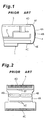
- Fig. 1 is a sectional view illustrating a structure for supporting a drive circuit board provided for driving a flat display panel of a conventional flat display apparatus for generation of an image.
- the flat display apparatus has a flat display panel 1 supported by a chassis 2, and a drive circuit board 3 mounted on the rear face of the chassis 2 and supported parallel to the flat display panel 1.
- the drive circuit board 3 is connected to the flat display panel 1 by a wiring board (e.g. TCP: Tape Carrier Package) 4 curving around a side of the chassis 2.
- a wiring board e.g. TCP: Tape Carrier Package
- the wiring board 4 has a driver integrated circuit 4B fixed in a substantially central portion of a plate-shaped board body 4A, an electrode terminal 4C formed in one edge (the lower edge in Fig. 2) of the board body 4A and connected to the flat display panel 1, and an electrode terminal 4D formed in the other edge (the upper edge in Fig. 2) and connected to the drive circuit board 3.
- the wiring board 4 further has a flection 4E extending in a portion parallel to the electrode terminal 4C between the driver integrated circuit 4B and the electrode terminal 4C on the board body 4A.
- the flection 4E enables the bending of the board body 4A.
- a flection 4F extends in parallel to the electrode terminal 4D in a portion between the driver integrated circuit 4B and the electrode terminal 4D.
- the wiring board 4 is placed in front of the lateral end of the chassis 2 in a position approximately right angles to the flat display panel.
- the wiring board 4 is then bent at the flections 4E so that the electrode terminal 4C becomes parallel to the flat display panel 1.
- the electrode terminal 4C is connected to an electrode terminal of the'flat display panel 1 by means of thermo-compression bonding.
- the wiring board 4 is also bent at the flections 4F so that the electrode terminal 4D becomes parallel to the drive circuit board 3.
- the electrode terminal 4D is connected to an electrode terminal of the drive circuit board 3 by means of thermo-compression bonding.
- the flat display panel 1 and the drive circuit board 3 are arranged in parallel to each other with the chassis 2 in between.
- the wiring board 4 is placed in front of the lateral end of the chassis 2 in a position approximately at right angles to the flat display panel 1 so as to straddle the chassis 2 for establishing a connection between the flat display panel 1 and the drive circuit board 3.
- the thickness of the chassis 2 causes an increase not only in the space between the flat display panel 1 and the drive circuit board 3, but also in the length of the wiring board 4, making unnecessary the use of an expensive wiring board 4.
- the use of an expensive wiring board is a factor in the increase of the production costs.
- the present invention has been made to solve the problem associatedwiththeconventionalflatdisplayapparatusasdescribed above.
- the present invention provides a flat display apparatus including: a flat display panel; a chassis member for supporting the flat display panel from the rear; a drive circuit board provided for the flat display panel; and a wiring member having a first electrode terminal connected to the flat display panel, and a second electrode terminal connected to the drive circuit board, to establish a connection between the flat display panel and the drive circuit board.
- the flat display apparatus has the advantages of: placing the drive circuit board in a side portion of the chassis member at an angle to the flat display panel, and forming bendable portions in a plurality of positions of the wiring member to enable free bending of the wiring member, in which the wiring member is mounted in a front corner of the flat display apparatus and between the flat display panel and the drive circuit board which are mounted at an angle to each other on the chassis member, in such a way that the first electrode terminal and the second electrode terminal are respectively connected to the flat display panel and the drive circuit board, and a portion of the wiring member between the first electrode terminal and the second electrode terminal is bent in a direction of projecting toward the front of the flat display panel by use of the bendable portions formed in the plurality of positions.
- the flat display apparatus includes a chassis member for supporting a flat display panel such as a PDP, FED, liquid crystal panel or the like.
- a drive circuit board for driving the flat display panel and controlling the driving is mounted on the chassis in a direction of forming an angle with respect to the flat display panel, namely, in a direction at right angles or an oblique angle to the flat display panel.
- a wiring board having a driver integrated circuit or a wiring member such as a flexible cable is mounted so as to connect the first electrode terminal to the flat display panel and the second electrode terminal to the drive circuit board for forming the connection between the flat display panel and the drive circuit board.
- the wiring member is bent by use of bendable portions formed in a plurality of positions of the wiring member such that part of the member body between the first electrode terminal and the second electrode terminal projects in the direction of the front of the flat display panel.
- the drive wiring board is supported by the chassis member in a position forming an angle with the flat display panel, and the wiring member establishes the connection between the drive wiring board and the flat display panel in the front side corner of the flat display apparatus.
- This structure enables the connection of the flat display panel and the drive circuit board over the shortest possible distance, thereby decreasing the length of the wiring member as compared with a conventional wiring member. As a result it is possible to reduce the parts cost of an expensive wiring member to lower production costs.
- the connection of the flat display panel and the drive circuit board is established in the form of making an allowance. Due to this allowance, even when, for example, the positional relationship between the flat display panel and the drive circuit board is changed by deformation, displacement or the like of the chassis, the wiring board is prevented from being damaged and the electrode terminals maintain their connection. Accordingly, it is possible to improve the reliability of production quality.
- Fig. 3 is a plane cross' sectional view illustrating the structure of one lateral end of a flat display apparatus according to a first embodiment of the present invention.
- a chassis 10 supports a flat display panel 1 and has an outer face 10A of a lateral end formed in a plane shape extending in a direction at right angles to the flat display panel 1.
- a drive circuit board 11 is mounted on the outer face 10A of the chassis 10 by the interposition of a mounting fixture 12, and positioned parallel to the outer face 10A, namely, at right angles to the flat display panel 1.
- the drive circuit board 11 mounted on the outer face 10A of the chassis 10 is connected through a wiring board 13 to the flat display panel 1 supported on the front surface of the chassis 10.
- the wiring board 13, as illustrated in Fig. 4, has an electrode terminal 13B formed in one edge (the lower edge in Fig. 4) of a plate-shaped board body 13A and connected to the flat display panel 1, and an electrode terminal 13C formed in the other edge (the upper edge in Fig. 4) and connected to the drive circuit board 11.
- a flection 13DA enabling the bending of the board body 13A is formed in an approximately central portion of the board body 13A and extends in the width direction of the board body 13A (in the right-left direction in Fig. 4).
- a flection 13DB is also formed parallel to the flection 13DA in the portion of the board body 13A on the electrode terminal 13B side with respect to the flection 13DA.
- a driver integrated circuit 13E is seated in the portion of the board body 13A between the flection 13DA and the electrode terminal 13C.
- Fig. 5 is a sectional view taken along the line V-V line on the wiring board 13 in Fig. 4.
- the board body 13A of the wiring board 13 is constituted of an insulation resin plate (polyimide tape in the first embodiment) 13Aa, a wiring pattern 13Ab of a copper wire formed on the insulation resin plate 13Aa, and an insulating layer 13Ac covering the wiring pattern 13Ab.
- each of the flections 13DA and 13DB of the wiring board 13 the part of the insulation resin plate 13Aa corresponding to the flection is removed in a strip shape, and then a thin coat of another insulation resin 13Da is applied to the exposed part.
- one electrode terminal 13B of the wiring board 13 is connected to the electrode terminal of the flat display panel 1 by means of thermo-compression bonding, and the other electrode terminal 13C is connected to the electrode terminal of the drive circuit board 11 by means of thermo-compression bonding, whereby the wiring board 13 establishes a connection between the flat display panel 1 and the drive circuit board 11.
- the board body 13A of the wiring board 13 is bent toward the front of the flat display panel 1 in the flection 13DB situated close to the electrode terminal 13B. Further, the board body 13A is again bent, in the flection 13DA situated approximately in the central portion of the board body 13A, in the direction of the rear of the flat display panel 1 to become parallel to the drive circuit board 11.
- the wiring board 13 is mounted between the flat display panel 1 and the drive circuit board 11 which are positioned at right angles to each other, thus making the approximately central portion of the board body 13A project toward the front of the flat display panel 1.
- the wiring board 13 is mounted in such a way that the approximately central portion of the wiring board 13 projects toward the front side of the flat display panel 1 as illustrated in Fig. 3. Due to this way of mounting, even when the chassis 10 is inclined with respect to the flat display panel 1 during the manufacturing process or by deformation of the chassis 10 caused by warping, deflection and the like, thus opening up a space between the side end of the flat display panel 1 and the side end of the chassis 10 as in the case of the illustration in Fig. 7, damage to the portion of the board body 13 around the electrode terminal 13B is avoided because of the allowance created by bending the approximately central portion of the wiring board 13 to project in the direction of the front side of the flat display panel 1, as illustrated in Fig. 9.
- the flat display panel 1 and the drive circuit board 11 are able to be connected over the shortest possible distance, so that it is possible to decrease the length of the wiring board 13 as compared with a conventional wiring board to reduce the parts cost of the expensive wiring board 13 for lowering production costs.
- the wiring board 13 is prevented from being damaged and the electrode terminals maintain their connection. Accordingly, it is possible to improve the reliability of production quality
- Fig. 11 is a plane cross sectional view illustrating the structure of one lateral end portion of a flat display apparatus in a second embodiment according to the present invention.
- a drive circuit board 11 is mounted on an outer face 20A of a chassis 20 supporting a flat display panel 1.
- the outer face 20A is inclined steadily inward (the left-hand direction in Fig. 11) with respect to the flat display panel 1 as it extends in the direction of the rear of the flat display panel 1 (the upper direction in Fig. 11).
- the wiring board 23 is supported by the mounting fixtures 12 so as to be in parallel to the outer face 20A of a side end of the chassis 20, namely, so as to be inclined in the same direction as that of the outer face 20A with respect to the flat display panel 1.
- the drive circuit board 11 mounted on the outer face 20A of the chassis 20 and the flat display panel 1 supported on the front face of the chassis 20 are connected to each other by a wiring board 23.
- the wiring board 23 has an electrode terminal 23B formed at one edge (the lower edge in Fig. 12) of a plate-shaped board body 23A, and an electrode terminal 23C formed at the other edge (the upper edge in Fig. 12).
- the electrode terminal 23B is connected to the flat display panel 1, and the electrode terminal 23C to the drive circuit board 11.
- a f lection 23DA enabling the bending of the board body 23A is formed in an approximately central portion of the board body 23A and extends in the width direction of the board body 23A (in the right-left direction in Fig. 12).
- a flection 23DB is also formed parallel to the flection 23DA in a portion of the board body 23A on the electrode terminal 23B side with respect to the flection 23DA.
- a flection 23DC is formed in parallel to the flection 23DA in a portion of the board body 23A on the electrode terminal 23C side with respect to the flection 23DA.
- a driver integrated circuit 23E is seated in a portion of the board body 23A between the flection 23DA and the electrode terminal 23C.
- the method of forming the flections 23DA, 23DB and 23DC is similar to the method described in Fig. 5 in the first embodiment.
- one electrode terminal 23B of the wiring board 23 is connected to the electrode terminal of the flat display panel 1 by means of thermo-compression bonding, and the other electrode terminal 23C is connected to the electrode terminal of the drive circuit board 11 by means of thermo-compression bonding, whereby the wiring board 23 establishes a connection between the flat display panel 1 and the drive circuit board 11.
- the board body 23A of the wiring board 23 is bent toward the front of the flat display panel 1 in the flection 23DB situated close to the electrode terminal 23B, then bent approximately at right angles toward the rear of the flat display panel 1 in the flection 23DA situated approximately in the central portion of the board body 23A, and then bent toward the inside (toward the chassis 20) in the flection 23DC.
- the flat display apparatus in the second embodiment is capable of connecting the flat display panel 1 and the drive circuit board 11 over the shortest possible distance. Therefore, it is possible to decrease the length of the wiring board 23 as compared with a conventional wiring board to reduce the parts cost of the expensive wiring board 23 for achieving low cost.
- the wiring board 23 is prevented from being damaged and the electrode terminals maintain their connection. Accordingly, it is possible to improve the reliability of production quality.
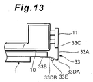
- Fig. 13 is a plane cross sectional view illustrating the structure of one lateral end portion of a flat display apparatus in a third embodiment according to the present invention.
- a drive circuit board 11 is placed in a position approximately at right angles to the flat display panel 1 as in the case of the first embodiment described in Fig. 3, and connected through a wiring board 33 to the flat display panel 1.
- a board body 33A of the wiring board 33 is bent toward the front of the flat display panel 1 in a flection 33DB situated close to an electrode terminal 33B, and then bent, in a flection 33DA situated approximately in the central portion of the board body 33A, toward the rear of the flat display panel 1 to become parallel to the drive circuit board 11, in order to establish a connection between the flat display panel 1 and the drive circuit board 11 as in the case of the first embodiment described in Fig. 3.
- a point of difference from the case of the first embodiment is that a drive integrated circuit 33E is installed in a portion between the flax portions 33DA and 33DB of the board body 33A.
- a generic concept of the flat display apparatus in the foregoing embodiments is a flat display apparatus including: a flat display panel; a chassis member for supporting the flat display panel from the rear; a drive circuit board provided for the flat display panel; and a wiring member having a first electrode terminal connected to the flat display panel, and a second electrode terminal connected to the drive circuit board, to establish a connection between the flat display panel and the drive circuit board.
- the drive circuit board is placed in a side portion of the chassis member at an angle to the flat display panel.
- the wiring member further has bendable portions formed in a plurality of positions of the wiring member to enable free bending of the wiring member.
- the wiring member is mounted in a front corner of the flat display apparatus and between the flat display panel and the drive circuit board which are mounted at an angle to each other on the chassis member, in such a way that the first electrode terminal and the second electrode terminal are respectively connected to the flat display panel and the drive circuit board, and a portion of the wiring member between the first electrode terminal and the second electrode terminal is bent in a direction of projecting toward the front of the flat display panel by use of the bendable portions formed in the plurality of positions.
- the flat display apparatus of an embodiment forming the generic concept includes a chassis member for supporting a flat display panel such as a PDP, FED, liquid crystal panel or the like.
- a drive circuit board for driving the flat display panel and controlling the driving is mounted on the chassis in a direction of forming an angle with respect to the flat displaypanel, namely, in a direction at right angles or an oblique angle to the flat display panel.
- a wiring board having a driver integrated circuit or a wiring member such as a flexible cable is mounted so as to connect the first electrode terminal to the flat display panel and the second electrode terminal to the drive circuit board for forming the connection between the flat display panel and the drive circuit board.
- the wiring member is bent by use of bendable portions formed in a plurality of positions of the wiring member such that part of the member body between the first electrode terminal and the second electrode terminal projects in the direction of the front of the flat display panel.
- the drive wiring board is supported by the chassis member in a position forming an angle with the flat display panel, and the wiring member establishes the connection between the drive wiring board and the flat display panel in the front side corner of the flat display apparatus.
- This structure enables the connection of the flat display panel and the drive circuit board over the shortest possible distance, thereby decreasing the length of the wiring member as compared with a conventional wiring member. As a result it is possible to reduce the parts cost of an expensive wiring member to lower production costs.
- the connection of the flat display panel and the drive circuit board is established in the form of making an allowance. Due to this allowance, even when, for example, the positional relationship between the flat display panel and the drive circuit board is changed by deformation, displacement or the like of the chassis, the wiring board is prevented from being damaged and the electrode terminals maintain their connection. Accordingly, it is possible to improve the reliability of production quality.
Landscapes
- Engineering & Computer Science (AREA)
- Microelectronics & Electronic Packaging (AREA)
- Devices For Indicating Variable Information By Combining Individual Elements (AREA)
- Liquid Crystal (AREA)
Abstract
Description
Claims (9)
- A flat display apparatus including:characterized in thata flat display panel (1);a chassis member (10) for supporting the flat display panel (1) from the rear of the flat display panel (1);a drive circuit board (11) provided for the flat display panel (1); anda wiring member (13) having a first electrode terminal (13B) connected to the flat display panel (1), and a second electrode terminal (13C) connected to the drive circuit board (11), to establish a connection between the flat display panel (1) and the drive circuit board (11)
the drive circuit board (11) is placed in a side portion of the chassis member (10) at an angle to the flat display panel (1);
the wiring member (13) has bendable portions (13DA, 13DB) formed in a plurality of positions of the wiring member (13) to enable free bending of the wiring member (13); and
the wiring member (13) is mounted in a front corner of the flat display apparatus and between the flat display panel (1) and the drive circuit board (11) which are mounted at an angle to each other on the chassis member (10), in such a way that the first electrode terminal (13B) and the second electrode terminal (13C) are respectively connected to the flat display panel (1) and the drive circuit board (11), and a portion of the wiring member (13) between the first electrode terminal (13B) and the second electrode terminal (13C) is bent in a direction of projecting toward the front of the flat display panel (1) by use of the bendable portions (13DA, 13DB) formed in the plurality of positions. - A flat display apparatus according to claim 1, wherein the wiring member (13) has an insulation resin layer (13Aa), a metal-made wiring pattern (13Ab) formed on the insulation resin layer (13Aa), and an insulating layer (13Ac) covering the wiring pattern (13Ab), and the bendable portion (13DA, 13DB) is formed by removing a part of the insulation resin layer (13Aa)
- A flat display apparatus according to claim 2, wherein the insulation resin layer (13Aa) is formed of a polyimide tape.
- A flat display apparatus according to any of claims 1 to 3, wherein the bendable portions (13DA, 13DB) are formed in at least two positions, namely a portion in the proximity of the first electrode terminal (13B) of the wiring member (13) and a portion between the first electrode terminal (13B) and the second electrode terminal (13C).
- A flat display apparatus according to any of claims 1 to 4, wherein the bendable portions (23DA, 23DB, 23DC) are formed in at least three positions, namely a portion in the proximity of the first electrode terminal (23B) of the wiring member (23), a portion in the proximity of the second electrode terminal (23C), and a portion situated between the portion in the proximity of the first electrode terminal (23B) and the portion in the proximity of the second electrode (23C).
- A flat display apparatus according to any of claims 1 to 4, wherein the wiring member (13) further includes a driver integrated circuit (13E) placed between the second electrode terminal (13C) and the bendable portion (13DA) formed between the first electrode terminal (13B) and the second electrode terminal (13C).
- A flat display apparatus according to any of claims 1 to 4, wherein the wiring member (23) further includes a driver integrated circuit (23E) placed between the first electrode terminal (23B) and the bendable portion (23DC) formed between the first electrode terminal (23B) and the second electrode terminal (23C).
- A flat display apparatus according to any of claims 1 to 7, wherein the flat display panel (1) is either of a plasma display panel or a field emission display panel, and the wiring member is a wiring board (13) having a driver integrated circuit (13E).
- A flat display apparatus according to any of claims 1 to 8, wherein the flat display panel (1) is a liquid crystal panel and the wiring member (13) is a flexible, cable.
Applications Claiming Priority (2)
| Application Number | Priority Date | Filing Date | Title |
|---|---|---|---|
| JP2002362787A JP2004191867A (en) | 2002-12-13 | 2002-12-13 | Flat display device |
| JP2002362787 | 2002-12-13 |
Publications (2)
| Publication Number | Publication Date |
|---|---|
| EP1457809A2 true EP1457809A2 (en) | 2004-09-15 |
| EP1457809A3 EP1457809A3 (en) | 2004-11-24 |
Family
ID=32501074
Family Applications (1)
| Application Number | Title | Priority Date | Filing Date |
|---|---|---|---|
| EP03027470A Withdrawn EP1457809A3 (en) | 2002-12-13 | 2003-12-01 | Flat display apparatus |
Country Status (3)
| Country | Link |
|---|---|
| US (1) | US6977709B2 (en) |
| EP (1) | EP1457809A3 (en) |
| JP (1) | JP2004191867A (en) |
Families Citing this family (11)
| Publication number | Priority date | Publication date | Assignee | Title |
|---|---|---|---|---|
| KR100637149B1 (en) * | 2004-02-20 | 2006-10-20 | 삼성에스디아이 주식회사 | Plasma display device |
| JP4280726B2 (en) * | 2004-06-29 | 2009-06-17 | キヤノン株式会社 | Image display device |
| JP4599117B2 (en) * | 2004-08-27 | 2010-12-15 | パナソニック株式会社 | Plasma display device |
| KR100784564B1 (en) * | 2005-05-19 | 2007-12-11 | 엘지전자 주식회사 | Plasma display |
| US8077448B2 (en) * | 2005-05-19 | 2011-12-13 | Lg Electronics Inc. | Plasma display apparatus |
| KR100696834B1 (en) | 2005-09-06 | 2007-03-19 | 삼성에스디아이 주식회사 | Plasma Display with Curved Chassis Base |
| KR101366535B1 (en) | 2007-03-23 | 2014-02-27 | 삼성디스플레이 주식회사 | Backlight assembly, display module having the backlight assembly and method of manufacturing receiving container receiving the backlight assembly |
| JP2009069610A (en) * | 2007-09-14 | 2009-04-02 | Bridgestone Corp | Information display panel |
| CN101472386B (en) * | 2007-12-26 | 2012-03-28 | 鸿富锦精密工业(深圳)有限公司 | Printed circuit board |
| JP2015005538A (en) * | 2013-06-19 | 2015-01-08 | 京セラ株式会社 | Flexible substrate and electronic device having the same |
| JP6331887B2 (en) * | 2014-08-29 | 2018-05-30 | 日本精機株式会社 | Display device |
Family Cites Families (12)
| Publication number | Priority date | Publication date | Assignee | Title |
|---|---|---|---|---|
| US4851613A (en) * | 1988-06-08 | 1989-07-25 | Flex Technology, Inc. | Flexible circuit laminate for surface mount devices |
| JP3610077B2 (en) * | 1992-03-26 | 2005-01-12 | セイコーエプソン株式会社 | Liquid crystal display device and electronic device |
| US5831828A (en) * | 1993-06-03 | 1998-11-03 | International Business Machines Corporation | Flexible circuit board and common heat spreader assembly |
| US5841414A (en) * | 1994-08-16 | 1998-11-24 | Citizen Watch Co., Ltd. | Liquid crystal display device |
| US5748269A (en) * | 1996-11-21 | 1998-05-05 | Westinghouse Air Brake Company | Environmentally-sealed, convectively-cooled active matrix liquid crystal display (LCD) |
| JP3659810B2 (en) | 1998-08-05 | 2005-06-15 | パイオニア株式会社 | Two-dimensional display unit drive module mounting structure |
| KR100304256B1 (en) * | 1998-08-26 | 2002-07-18 | 윤종용 | Display Module of LCD and Assembly Method |
| TW550428B (en) * | 1999-07-12 | 2003-09-01 | Nec Lcd Technologies Ltd | Flat panel display device and manufacturing method thereof |
| DE19941514A1 (en) * | 1999-08-31 | 2001-03-01 | Mannesmann Vdo Ag | Liquid crystal display |
| JP3662788B2 (en) * | 1999-10-06 | 2005-06-22 | Nec液晶テクノロジー株式会社 | Liquid crystal display device and portable information terminal device |
| US20020186551A1 (en) * | 2000-02-24 | 2002-12-12 | Toru Murowaki | Electronic control unit having flexible wires connecting connector to circuit board |
| JP2003243778A (en) | 2002-02-15 | 2003-08-29 | Matsushita Electric Ind Co Ltd | Flexible wiring board and liquid crystal display device having flexible wiring board |
-
2002
- 2002-12-13 JP JP2002362787A patent/JP2004191867A/en active Pending
-
2003
- 2003-12-01 US US10/724,120 patent/US6977709B2/en not_active Expired - Fee Related
- 2003-12-01 EP EP03027470A patent/EP1457809A3/en not_active Withdrawn
Also Published As
| Publication number | Publication date |
|---|---|
| US6977709B2 (en) | 2005-12-20 |
| US20040114063A1 (en) | 2004-06-17 |
| JP2004191867A (en) | 2004-07-08 |
| EP1457809A3 (en) | 2004-11-24 |
Similar Documents
| Publication | Publication Date | Title |
|---|---|---|
| CN207183276U (en) | Display device | |
| US7187427B2 (en) | Flat panel type display apparatus | |
| US6977709B2 (en) | Flat display apparatus | |
| US20180376596A1 (en) | Printed circuit board unit display apparatus and method of manufacturing the display apparatus | |
| US8779292B2 (en) | Substrate and substrate bonding device using the same | |
| JP5528906B2 (en) | Display device | |
| US7004761B2 (en) | Display apparatus and connecting cables used in the display apparatus | |
| US8053988B2 (en) | Plasma display device | |
| JP2002299773A (en) | Flexible wiring board and electro-optical device | |
| JP6762196B2 (en) | Electro-optic display | |
| JP2007103431A (en) | Wiring board and semiconductor device | |
| US20220225505A1 (en) | Display panel and display device having same | |
| US8011989B2 (en) | Method of making a plasma display panel with a novel connection structure | |
| CN116454605A (en) | Wall-mounted antenna and method for manufacturing wall-mounted antenna | |
| CN114300484A (en) | Display panel, display device and manufacturing method of display panel | |
| US10966320B2 (en) | Gap supporter for printed circuit board, and package including gap supporter for printed circuit board and insulation sheet coupled thereto | |
| US20090246477A1 (en) | Assembly structure | |
| CN111221182A (en) | Backlight source and preparation method thereof | |
| US7591671B2 (en) | Connector for display device | |
| US12100700B2 (en) | Light-emitting diode panel and spliced panel | |
| JP4660007B2 (en) | Display device | |
| CN219266729U (en) | Display panel and electronic terminal | |
| CN119233682A (en) | Display panel, preparation method thereof, display module and display device | |
| CN116978288A (en) | Display screen, display screen manufacturing method and spliced screen | |
| JP2006128167A (en) | Electronic apparatus and flexible printed circuit board |
Legal Events
| Date | Code | Title | Description |
|---|---|---|---|
| PUAI | Public reference made under article 153(3) epc to a published international application that has entered the european phase |
Free format text: ORIGINAL CODE: 0009012 |
|
| AK | Designated contracting states |
Kind code of ref document: A2 Designated state(s): AT BE BG CH CY CZ DE DK EE ES FI FR GB GR HU IE IT LI LU MC NL PT RO SE SI SK TR |
|
| AX | Request for extension of the european patent |
Extension state: AL LT LV MK |
|
| PUAL | Search report despatched |
Free format text: ORIGINAL CODE: 0009013 |
|
| AK | Designated contracting states |
Kind code of ref document: A3 Designated state(s): AT BE BG CH CY CZ DE DK EE ES FI FR GB GR HU IE IT LI LU MC NL PT RO SE SI SK TR |
|
| AX | Request for extension of the european patent |
Extension state: AL LT LV MK |
|
| RIC1 | Information provided on ipc code assigned before grant |
Ipc: 7H 01R 12/04 B Ipc: 7G 02F 1/13 A |
|
| 17P | Request for examination filed |
Effective date: 20050103 |
|
| 17Q | First examination report despatched |
Effective date: 20050420 |
|
| AKX | Designation fees paid |
Designated state(s): DE FR GB |
|
| STAA | Information on the status of an ep patent application or granted ep patent |
Free format text: STATUS: THE APPLICATION HAS BEEN WITHDRAWN |
|
| 18W | Application withdrawn |
Effective date: 20060216 |