EP1455397A2 - Vertical MOS device and method of making the same - Google Patents
Vertical MOS device and method of making the same Download PDFInfo
- Publication number
- EP1455397A2 EP1455397A2 EP03029916A EP03029916A EP1455397A2 EP 1455397 A2 EP1455397 A2 EP 1455397A2 EP 03029916 A EP03029916 A EP 03029916A EP 03029916 A EP03029916 A EP 03029916A EP 1455397 A2 EP1455397 A2 EP 1455397A2
- Authority
- EP
- European Patent Office
- Prior art keywords
- layer
- channel
- gate oxide
- thicker
- oxide
- Prior art date
- Legal status (The legal status is an assumption and is not a legal conclusion. Google has not performed a legal analysis and makes no representation as to the accuracy of the status listed.)
- Withdrawn
Links
Images



Classifications
-
- H—ELECTRICITY
- H10—SEMICONDUCTOR DEVICES; ELECTRIC SOLID-STATE DEVICES NOT OTHERWISE PROVIDED FOR
- H10D—INORGANIC ELECTRIC SEMICONDUCTOR DEVICES
- H10D30/00—Field-effect transistors [FET]
- H10D30/60—Insulated-gate field-effect transistors [IGFET]
- H10D30/64—Double-diffused metal-oxide semiconductor [DMOS] FETs
- H10D30/66—Vertical DMOS [VDMOS] FETs
-
- H—ELECTRICITY
- H10—SEMICONDUCTOR DEVICES; ELECTRIC SOLID-STATE DEVICES NOT OTHERWISE PROVIDED FOR
- H10D—INORGANIC ELECTRIC SEMICONDUCTOR DEVICES
- H10D30/00—Field-effect transistors [FET]
- H10D30/01—Manufacture or treatment
- H10D30/021—Manufacture or treatment of FETs having insulated gates [IGFET]
- H10D30/028—Manufacture or treatment of FETs having insulated gates [IGFET] of double-diffused metal oxide semiconductor [DMOS] FETs
- H10D30/0291—Manufacture or treatment of FETs having insulated gates [IGFET] of double-diffused metal oxide semiconductor [DMOS] FETs of vertical DMOS [VDMOS] FETs
-
- H—ELECTRICITY
- H10—SEMICONDUCTOR DEVICES; ELECTRIC SOLID-STATE DEVICES NOT OTHERWISE PROVIDED FOR
- H10D—INORGANIC ELECTRIC SEMICONDUCTOR DEVICES
- H10D30/00—Field-effect transistors [FET]
- H10D30/60—Insulated-gate field-effect transistors [IGFET]
- H10D30/64—Double-diffused metal-oxide semiconductor [DMOS] FETs
- H10D30/66—Vertical DMOS [VDMOS] FETs
- H10D30/662—Vertical DMOS [VDMOS] FETs having a drift region having a doping concentration that is higher between adjacent body regions relative to other parts of the drift region
-
- H—ELECTRICITY
- H10—SEMICONDUCTOR DEVICES; ELECTRIC SOLID-STATE DEVICES NOT OTHERWISE PROVIDED FOR
- H10D—INORGANIC ELECTRIC SEMICONDUCTOR DEVICES
- H10D62/00—Semiconductor bodies, or regions thereof, of devices having potential barriers
- H10D62/10—Shapes, relative sizes or dispositions of the regions of the semiconductor bodies; Shapes of the semiconductor bodies
- H10D62/13—Semiconductor regions connected to electrodes carrying current to be rectified, amplified or switched, e.g. source or drain regions
- H10D62/149—Source or drain regions of field-effect devices
- H10D62/151—Source or drain regions of field-effect devices of IGFETs
-
- H—ELECTRICITY
- H10—SEMICONDUCTOR DEVICES; ELECTRIC SOLID-STATE DEVICES NOT OTHERWISE PROVIDED FOR
- H10D—INORGANIC ELECTRIC SEMICONDUCTOR DEVICES
- H10D64/00—Electrodes of devices having potential barriers
- H10D64/20—Electrodes characterised by their shapes, relative sizes or dispositions
- H10D64/27—Electrodes not carrying the current to be rectified, amplified, oscillated or switched, e.g. gates
- H10D64/311—Gate electrodes for field-effect devices
- H10D64/411—Gate electrodes for field-effect devices for FETs
- H10D64/511—Gate electrodes for field-effect devices for FETs for IGFETs
- H10D64/514—Gate electrodes for field-effect devices for FETs for IGFETs characterised by the insulating layers
- H10D64/516—Gate electrodes for field-effect devices for FETs for IGFETs characterised by the insulating layers the thicknesses being non-uniform
Definitions
- the present invention relates, in its more general aspect, to vertical-conduction MOS power devices and to a method for realising them on an industrial scale with high integration density.
- the invention relates to a vertical-conduction and planar-structure MOS device with a double thickness of gate oxide.
- the invention also relates to a process for realising vertical-conduction MOS power devices starting from corresponding planar MOS structures.
- the present invention relates to a method for reducing the capacity of MOS devices of the type concerned, operating simultaneously and in a self-aligned way on corresponding planar MOS structures.
- the JFET resistance depends not only on the epitaxial layer resistivity but also on the distance between two adjacent body wells.
- the capacities associated to the gate oxide and thus the charge storage capacity of the gate region depend, in an opposite sense , on this distance.
- the following table 1 shows a comparison between the relative weight of the output resistance components of a 30-volt P-channel device.
- Output resistance components for a 30-volt P-channel PMOS device Relative weight Die-package connection 25%
- the methods a) and b) applied to low voltage PMOS devices involve known technical drawbacks linked to the influence of the enriched layer on the channel.
- the gate area is proportional to the distance L (1.5-4 ⁇ m) while in the case of a trench technology device it is proportional to the sum of the double depth and of the trench width (2h+1 ⁇ 2.5-4 ⁇ m).
- the technical problem underlying the present invention is to provide a method for realising vertical-conduction MOS power devices having improved static and dynamic performances with respect to prior art devices, as well as capable of reducing the capacities of these devices for the same static performances.
- the solution idea underlying the present invention is to use a double thickness of gate oxide, a thin layer in the channel region and a thicker layer on inactive areas. In the meantime, it provides an enrichment of the JFET region in order to reduce the distance between the body regions and to increase the integration area reducing the extension of the gate oxide surface.
- MOS transistor electronic device particularly of the PMOS type, according to the method of the present invention is globally and schematically indicated.
- the transistor device 1 is obtained from a semiconductor substrate 2 covered by an oxide protective layer.
- the method of the present invention is characterised in that it comprises the following operative steps:
- the method of the present invention is characterised in that it comprises the following operative steps:
- a metal layer for example of Ti, W or Co
- conductive layer 12 it is also possible to use a metal layer (for example of Ti, W or Co) as conductive layer 12 to realise the gate electrode.
- the transistor obtained with the method according to the invention is a planar MOS with a double thickness of gate oxide, i.e. with a thinner oxide layer in the channel area and a thicker oxide layer in the central channel inactive area.
- the final MOS device comprises a gate oxide layer having thin oxide side portions 5a and a thick oxide central portion 5b, this thick oxide central portion 5b being in correspondence with the channel central inactive area.
- the final MOS device comprises a polysilicon layer 13 on the side portions 5a of the gate oxide layer.
- the enrichment region 9 in the JFET area underlying and self-aligned with the thicker oxide central portion 5a allows the distance between two adjacent body wells and thus the gate oxide surface to be reduced, obtaining an increased integration or packing density of the so-obtained transistors.
- Figures 8 shows the vertical section of a transistor realised according to the invention. This section has been obtained by means of process simulations wherein it is possible to see the gate oxide thickening and the enrichment layer position. Figure 8 also shows the concentration profile along the central line between two body wells.
Landscapes
- Metal-Oxide And Bipolar Metal-Oxide Semiconductor Integrated Circuits (AREA)
Abstract
- a first portion (5a) of gate oxide having a lower thickness in a channel area close to the active areas (4), and a second portion (5b) of thicker gate oxide in a central area (11) on a JFET area and
- an enrichment region (9) in the JFET area under the second . portion (5b) of thicker gate oxide (11).
- realising the MOS transistor starting from a planar structure with a double thickness of gate oxide comprising a thin layer in the channel area close to the active areas (4) and a thicker layer in the central area (11) on the channel; and
- realising an enrichment region (9) in the JFET area below the thicker layer.
Description
| Output resistance components for a 30-volt P-channel PMOS device | Relative weight |
| Die-package connection | 25% |
| | 12% |
| | 12% |
| Contribution of the JFET between body wells | 33% |
| Component due to the | 18% |
| Ron | 100% |
- the drain is characterised by an epitaxial layer whose concentration ranges between 1 and 5*1016 at/cm3.
- gate oxides, because of the low threshold voltage (driving with Vg<4.5V) and of the low capacities required by the applications, have a thickness not lower than 200 Å and peak concentrations in the channel do not exceed 1017 at/cm3.
- realising on a planar MOS structure a double thickness for the gate oxide comprising a thin layer in the channel region of said structure, and a thicker layer in the inactive areas thereof and
- enriching, simultaneously and in a self-aligned way, the JFET area in order to reduce the distance between two adjacent body wells, reduce the gate oxide surface, obtaining an increased packing density.
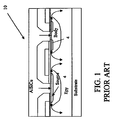
- Figure 1 is a vertical-section and enlarged-scale schematic view of a prior art traditional PMOS electronic device underlining the current flow direction during the operation condition;
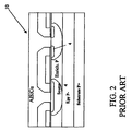
- Figure 2 is a vertical-section and enlarged-scale schematic view of a prior art surface-enriched PMOS electronic device;
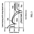
- Figure 3 shows on a doping concentration vs. channel width diagram a comparison between the PMOS devices of figures 1 and 2. In particular, it shows the surface enrichment influence on the concentration profile along the channel;
- Figure 4 compares the planar structure with the trench structure in an intermediate working step, both realised according to the prior art. It underlines, for both structures, the typical magnitudes on which the surface covered by the gate oxide depends;
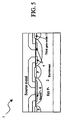
- Figure 5 is a vertical-section and enlarged-scale schematic view of a vertical MOS electronic device according to the present invention underlining the specific features introduced by the present invention (oxide thickening and corresponding enrichment of the epitaxial layer between body wells);
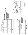
- Figures 6 are respective vertical-section and enlarged-scale schematic views of the PMOS device according to a first method of the invention undergoing different steps of the manufacturing method;
- Figures 7 are respective vertical-section and enlarged-scale schematic views of the PMOS device according to a second method of the invention undergoing different steps of the manufacturing method;
- Figure 8 shows on a diagram the vertical section of a transistor at an intermediate working step according to the invention and obtained by means of simulations of the method according to the invention.
Claims (14)
- A vertical-conduction and planar-structure MOS device having a double thickness of gate oxide characterised in that it comprises:a first portion (5a) of gate oxide having a lower thickness in a channel area close to the active areas (4), and a second portion (5b) of thicker gate oxide in a central area (11) on a JFET area andan enrichment region (9) in said JFET area under said second portion (5b) of thicker gate oxide (11).
- A MOS device according to claim 1, characterised in that said enrichment region (9) is self-aligned with said second portion (5b) of thicker gate oxide.
- A MOS device according to claim 1, characterised in that said double thickness of gate oxide globally has a reduced surface reducing the distance between adjacent body wells enveloping said active areas (4).
- A MOS device according to claim 1, characterised in that it comprises a polysilicon layer (13) on said first portion (5a) of thin gate oxide.
- A MOS device according any of the previous claims, characterised in that it comprises respective first portions (5a) of thin gate oxide at the periphery of said second portion (5b) of thicker gate oxide.
- A method for realising on a semiconductor substrate (2) MOS transistor (1) electronic devices with improved static and dynamic performances and high scaling down density, said transistors having traditional active areas (4) defined in the substrate (2) at the periphery of a channel region whereon a gate region is realised, characterised in that it comprises at least the steps of:realising the MOS transistor starting from a planar structure with a double thickness of gate oxide comprising a thin layer in the channel area close to the active areas (4) and a thicker layer in the central area (11) on the channel; andrealising an enrichment region (9) in the JFET area below said thicker layer.
- A method according to claim 6, characterised in that said enrichment region (9) is realised in parallel and in a self-aligned way with said thicker oxide layer.
- A method according to claim 6, characterised in that said double thickness of gate oxide globally has a reduced surface reducing the distance between adjacent body wells enveloping said active areas (4).
- A method according to claim 6, characterised in that, after defining the active areas (4) at the periphery of the channel region, it comprises the following operating steps:growing a pad oxide (5) on the active areas (4) and on the channel for a thickness of about 100-500 A;depositing a nitride layer (6) of 300-900 A on the oxide layer (5);photomasking to define the inactive areas (11) which must have a thicker oxide layer;etching the nitride layer (6) removing the same on the channel up to expose the oxide layer (5);further implanting to realise said enrichment region (9) in the channel central area using the photoresist as implant window;removing the photoresist and growing said first thicker gate oxide layer (8);etching the nitride layer (6);selectively etching to remove also the oxide layer (5) on the active areas (4);growing a sacrificial oxide layer;wet etching this sacrificial oxide layer to expose the gate region of the transistor (1) on the channel;growing a second gate oxide layer at the periphery of the thicker oxide area (11).
- A method according to claim 9, characterised in that said implant step is performed with P, As or Sb ions for a N-channel transistor and B or Al ions for a P-channel transistor, the implant energy is regulated between 60-900 KeV while ion doses can range from 1E12 and 1E13 ions/cm2.
- A method according to claim 6, characterised in that, after defining the active areas (4) at the periphery of the channel region, comprises the following operating steps:growing the gate oxide on the active areas (4) and on the channel for the thickness required for the device correct operation (100-1500 A);depositing a polysilicon layer (13) having a thickness being lower or equal to half the thickness of the thicker gate oxide part;depositing a nitride layer (6) of 300-900 A on the polysilicon layer (13);photomasking to define the inactive areas (11) which must have a thicker oxide layer;etching the nitride layer (6) removing the same on the channel up to expose the polysilicon layer (13);further implanting to realise said enrichment region (9) in the channel central area using the photoresist as implant window;removing the photoresist and completely oxidising the polysilicon (13) not covered by the nitride layer (6);etching the nitride layer (6);depositing a conductive layer (12) to realise the gate electrode.
- A method according to claim 11, characterised in that said implant step is performed with P, As or Sb ions for a N-channel transistor and B or Al ions for a P-channel transistor, the implant energy is regulated between 60-900 KeV while ion doses can range from 1E12 and 1E13 ions/cm2.
- A method according to claim 11, characterised in that said conductive layer (12) to realise the gate electrode is composed of conveniently doped polysilicon.
- A method according to claim 11, characterised in that said conductive layer (12) to realise the gate electrode is composed of a metal layer.
Priority Applications (1)
| Application Number | Priority Date | Filing Date | Title |
|---|---|---|---|
| EP03029916A EP1455397A3 (en) | 2002-12-30 | 2003-12-29 | Vertical MOS device and method of making the same |
Applications Claiming Priority (3)
| Application Number | Priority Date | Filing Date | Title |
|---|---|---|---|
| EP02425803 | 2002-12-30 | ||
| EP02425803 | 2002-12-30 | ||
| EP03029916A EP1455397A3 (en) | 2002-12-30 | 2003-12-29 | Vertical MOS device and method of making the same |
Publications (2)
| Publication Number | Publication Date |
|---|---|
| EP1455397A2 true EP1455397A2 (en) | 2004-09-08 |
| EP1455397A3 EP1455397A3 (en) | 2005-08-17 |
Family
ID=32826763
Family Applications (1)
| Application Number | Title | Priority Date | Filing Date |
|---|---|---|---|
| EP03029916A Withdrawn EP1455397A3 (en) | 2002-12-30 | 2003-12-29 | Vertical MOS device and method of making the same |
Country Status (1)
| Country | Link |
|---|---|
| EP (1) | EP1455397A3 (en) |
Cited By (6)
| Publication number | Priority date | Publication date | Assignee | Title |
|---|---|---|---|---|
| US7800173B2 (en) | 2007-03-02 | 2010-09-21 | Stmicroelectronics, S.R.L. | Manufacturing process of a vertical-conduction MISFET device with gate dielectric structure having differentiated thickness and vertical-conduction MISFET device thus manufacture |
| US8158463B2 (en) | 2005-04-27 | 2012-04-17 | Stmicroelectronics S.R.L. | Process and method for manufacturing a MOS device with intercell ion implant using one or more parallel enrichment windows |
| WO2013128480A1 (en) * | 2012-02-28 | 2013-09-06 | Stmicroelectronics S.R.L. | Vertical semiconductor device and manufacturing process of the same |
| CN111200025A (en) * | 2018-11-20 | 2020-05-26 | 深圳尚阳通科技有限公司 | Superjunction device and method of making the same |
| CN112510080A (en) * | 2020-11-30 | 2021-03-16 | 西安微电子技术研究所 | Radiation reinforcing structure of anti-single-particle high-voltage MOS field effect transistor and preparation method |
| CN117954498A (en) * | 2023-12-29 | 2024-04-30 | 宜兴杰芯半导体有限公司 | A VDMOS structure with low on-resistance |
Family Cites Families (3)
| Publication number | Priority date | Publication date | Assignee | Title |
|---|---|---|---|---|
| DE3465225D1 (en) * | 1983-02-17 | 1987-09-10 | Nissan Motor | A vertical-type mosfet and method of fabricating the same |
| US5273922A (en) * | 1992-09-11 | 1993-12-28 | Motorola, Inc. | High speed, low gate/drain capacitance DMOS device |
| US5869371A (en) * | 1995-06-07 | 1999-02-09 | Stmicroelectronics, Inc. | Structure and process for reducing the on-resistance of mos-gated power devices |
-
2003
- 2003-12-29 EP EP03029916A patent/EP1455397A3/en not_active Withdrawn
Cited By (8)
| Publication number | Priority date | Publication date | Assignee | Title |
|---|---|---|---|---|
| US8158463B2 (en) | 2005-04-27 | 2012-04-17 | Stmicroelectronics S.R.L. | Process and method for manufacturing a MOS device with intercell ion implant using one or more parallel enrichment windows |
| US8324669B2 (en) | 2005-04-27 | 2012-12-04 | Stmicroelectronics S.R.L. | Process for manufacturing a MOS device with intercell ion implant confined to the gate electrode region |
| US7800173B2 (en) | 2007-03-02 | 2010-09-21 | Stmicroelectronics, S.R.L. | Manufacturing process of a vertical-conduction MISFET device with gate dielectric structure having differentiated thickness and vertical-conduction MISFET device thus manufacture |
| US7968412B2 (en) | 2007-03-02 | 2011-06-28 | Stmicroelectronics, S.R.L. | Manufacturing process of a vertical-conduction MISFET device with gate dielectric structure having differentiated thickness and vertical-conduction MISFET device thus manufacture |
| WO2013128480A1 (en) * | 2012-02-28 | 2013-09-06 | Stmicroelectronics S.R.L. | Vertical semiconductor device and manufacturing process of the same |
| CN111200025A (en) * | 2018-11-20 | 2020-05-26 | 深圳尚阳通科技有限公司 | Superjunction device and method of making the same |
| CN112510080A (en) * | 2020-11-30 | 2021-03-16 | 西安微电子技术研究所 | Radiation reinforcing structure of anti-single-particle high-voltage MOS field effect transistor and preparation method |
| CN117954498A (en) * | 2023-12-29 | 2024-04-30 | 宜兴杰芯半导体有限公司 | A VDMOS structure with low on-resistance |
Also Published As
| Publication number | Publication date |
|---|---|
| EP1455397A3 (en) | 2005-08-17 |
Similar Documents
| Publication | Publication Date | Title |
|---|---|---|
| CN100411191C (en) | Transistors and methods of forming them | |
| US7608512B2 (en) | Integrated circuit structure with improved LDMOS design | |
| US6518138B2 (en) | Method of forming Self-aligned lateral DMOS with spacer drift region | |
| US6277695B1 (en) | Method of forming vertical planar DMOSFET with self-aligned contact | |
| US7821063B2 (en) | Semiconductor device having enhanced performance and method | |
| US8089124B2 (en) | Lateral DMOS device and method for fabricating the same | |
| TWI420675B (en) | Semiconductor device with mask electrode and method thereof | |
| US20080224237A1 (en) | Semiconductor devices | |
| JP4970185B2 (en) | Semiconductor device and manufacturing method thereof | |
| US6465836B2 (en) | Vertical split gate field effect transistor (FET) device | |
| JPH09260651A (en) | Lateral field effect transistor and manufacturing method thereof | |
| CA2065242A1 (en) | Hot-carrier suppressed sub-micron misfet device | |
| US7067363B2 (en) | Vertical-conduction and planar-structure MOS device with a double thickness of gate oxide and method for realizing power vertical MOS transistors with improved static and dynamic performances and high scaling down density | |
| US6268626B1 (en) | DMOS field effect transistor with improved electrical characteristics and method for manufacturing the same | |
| US7517759B2 (en) | Method of fabricating metal oxide semiconductor device | |
| US6919605B2 (en) | Integrated circuit MOS transistor with reduced drain and source resistance | |
| US6506651B2 (en) | Semiconductor device and manufacturing method thereof | |
| US20050048707A1 (en) | Processing method for improving structure of a high voltage device | |
| US7122862B2 (en) | Reduction of channel hot carrier effects in transistor devices | |
| US20090114957A1 (en) | Semiconductor device and method of manufacturing the same | |
| JPH10144922A (en) | Field effect transistor (FET) and method for forming semiconductor field effect transistor | |
| KR100546496B1 (en) | Nonvolatile semiconductor memory device and manufacturing method thereof | |
| JP2004140059A (en) | Method of manufacturing insulated gate field effect transistor | |
| US20090096037A1 (en) | Semiconductor device having recessed field region and fabrication method thereof | |
| KR100573274B1 (en) | Field effect transistor and its manufacturing method |
Legal Events
| Date | Code | Title | Description |
|---|---|---|---|
| PUAI | Public reference made under article 153(3) epc to a published international application that has entered the european phase |
Free format text: ORIGINAL CODE: 0009012 |
|
| AK | Designated contracting states |
Kind code of ref document: A2 Designated state(s): AT BE BG CH CY CZ DE DK EE ES FI FR GB GR HU IE IT LI LU MC NL PT RO SE SI SK TR |
|
| AX | Request for extension of the european patent |
Extension state: AL LT LV MK |
|
| PUAL | Search report despatched |
Free format text: ORIGINAL CODE: 0009013 |
|
| AK | Designated contracting states |
Kind code of ref document: A3 Designated state(s): AT BE BG CH CY CZ DE DK EE ES FI FR GB GR HU IE IT LI LU MC NL PT RO SE SI SK TR |
|
| AX | Request for extension of the european patent |
Extension state: AL LT LV MK |
|
| 17P | Request for examination filed |
Effective date: 20060216 |
|
| AKX | Designation fees paid |
Designated state(s): DE FR GB IT |
|
| 17Q | First examination report despatched |
Effective date: 20080508 |
|
| STAA | Information on the status of an ep patent application or granted ep patent |
Free format text: STATUS: THE APPLICATION IS DEEMED TO BE WITHDRAWN |
|
| 18D | Application deemed to be withdrawn |
Effective date: 20081119 |