EP1453197A1 - Surface acoustic wave filter - Google Patents
Surface acoustic wave filter Download PDFInfo
- Publication number
- EP1453197A1 EP1453197A1 EP02767902A EP02767902A EP1453197A1 EP 1453197 A1 EP1453197 A1 EP 1453197A1 EP 02767902 A EP02767902 A EP 02767902A EP 02767902 A EP02767902 A EP 02767902A EP 1453197 A1 EP1453197 A1 EP 1453197A1
- Authority
- EP
- European Patent Office
- Prior art keywords
- surface acoustic
- comb
- electrode
- electrodes
- acoustic wave
- Prior art date
- Legal status (The legal status is an assumption and is not a legal conclusion. Google has not performed a legal analysis and makes no representation as to the accuracy of the status listed.)
- Granted
Links
Images





Classifications
-
- H—ELECTRICITY
- H03—ELECTRONIC CIRCUITRY
- H03H—IMPEDANCE NETWORKS, e.g. RESONANT CIRCUITS; RESONATORS
- H03H9/00—Networks comprising electromechanical or electro-acoustic elements; Electromechanical resonators
- H03H9/46—Filters
- H03H9/64—Filters using surface acoustic waves
-
- H—ELECTRICITY
- H03—ELECTRONIC CIRCUITRY
- H03H—IMPEDANCE NETWORKS, e.g. RESONANT CIRCUITS; RESONATORS
- H03H9/00—Networks comprising electromechanical or electro-acoustic elements; Electromechanical resonators
- H03H9/46—Filters
- H03H9/64—Filters using surface acoustic waves
- H03H9/6423—Means for obtaining a particular transfer characteristic
- H03H9/6433—Coupled resonator filters
- H03H9/644—Coupled resonator filters having two acoustic tracks
- H03H9/6456—Coupled resonator filters having two acoustic tracks being electrically coupled
- H03H9/6469—Coupled resonator filters having two acoustic tracks being electrically coupled via two connecting electrodes
-
- H—ELECTRICITY
- H03—ELECTRONIC CIRCUITRY
- H03H—IMPEDANCE NETWORKS, e.g. RESONANT CIRCUITS; RESONATORS
- H03H9/00—Networks comprising electromechanical or electro-acoustic elements; Electromechanical resonators
- H03H9/0023—Networks for transforming balanced signals into unbalanced signals and vice versa, e.g. baluns, or networks having balanced input and output
- H03H9/0028—Networks for transforming balanced signals into unbalanced signals and vice versa, e.g. baluns, or networks having balanced input and output using surface acoustic wave devices
- H03H9/0047—Networks for transforming balanced signals into unbalanced signals and vice versa, e.g. baluns, or networks having balanced input and output using surface acoustic wave devices having two acoustic tracks
- H03H9/0066—Networks for transforming balanced signals into unbalanced signals and vice versa, e.g. baluns, or networks having balanced input and output using surface acoustic wave devices having two acoustic tracks being electrically parallel
- H03H9/0071—Networks for transforming balanced signals into unbalanced signals and vice versa, e.g. baluns, or networks having balanced input and output using surface acoustic wave devices having two acoustic tracks being electrically parallel the balanced terminals being on the same side of the tracks
-
- H—ELECTRICITY
- H03—ELECTRONIC CIRCUITRY
- H03H—IMPEDANCE NETWORKS, e.g. RESONANT CIRCUITS; RESONATORS
- H03H9/00—Networks comprising electromechanical or electro-acoustic elements; Electromechanical resonators
- H03H9/02—Details
- H03H9/125—Driving means, e.g. electrodes, coils
- H03H9/145—Driving means, e.g. electrodes, coils for networks using surface acoustic waves
- H03H9/14517—Means for weighting
- H03H9/14529—Distributed tap
- H03H9/14535—Position weighting
-
- H—ELECTRICITY
- H03—ELECTRONIC CIRCUITRY
- H03H—IMPEDANCE NETWORKS, e.g. RESONANT CIRCUITS; RESONATORS
- H03H9/00—Networks comprising electromechanical or electro-acoustic elements; Electromechanical resonators
- H03H9/46—Filters
- H03H9/64—Filters using surface acoustic waves
- H03H9/6423—Means for obtaining a particular transfer characteristic
- H03H9/6433—Coupled resonator filters
- H03H9/6436—Coupled resonator filters having one acoustic track only
-
- H—ELECTRICITY
- H03—ELECTRONIC CIRCUITRY
- H03H—IMPEDANCE NETWORKS, e.g. RESONANT CIRCUITS; RESONATORS
- H03H9/00—Networks comprising electromechanical or electro-acoustic elements; Electromechanical resonators
- H03H9/46—Filters
- H03H9/64—Filters using surface acoustic waves
- H03H9/6423—Means for obtaining a particular transfer characteristic
- H03H9/6433—Coupled resonator filters
- H03H9/644—Coupled resonator filters having two acoustic tracks
- H03H9/6456—Coupled resonator filters having two acoustic tracks being electrically coupled
- H03H9/6469—Coupled resonator filters having two acoustic tracks being electrically coupled via two connecting electrodes
- H03H9/6476—Coupled resonator filters having two acoustic tracks being electrically coupled via two connecting electrodes the tracks being electrically parallel
-
- H—ELECTRICITY
- H03—ELECTRONIC CIRCUITRY
- H03H—IMPEDANCE NETWORKS, e.g. RESONANT CIRCUITS; RESONATORS
- H03H9/00—Networks comprising electromechanical or electro-acoustic elements; Electromechanical resonators
- H03H9/46—Filters
- H03H9/64—Filters using surface acoustic waves
- H03H9/6423—Means for obtaining a particular transfer characteristic
- H03H9/6433—Coupled resonator filters
- H03H9/6483—Ladder SAW filters
Definitions
- the present invention relates to a low insertion loss surface acoustic wave (SAW) filter having a wide bandwidth characteristics.
- SAW surface acoustic wave
- the surface acoustic wave filter is employed in a radio-frequency (RF) circuit section of the cellular phone.
- RF radio-frequency
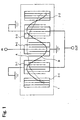
- FIG. 1 shows a plan view of an exemplary structure of a conventional surface acoustic wave filter.
- the surface acoustic wave filter has a pair of reflective electrodes 2-1, 2-2 on a piezoelectric substrate 1 formed of LiTaO 3 , LiNbO 3 , etc.
- a plurality of comb electrodes (three electrodes in the example shown in FIG. 1) 3-1, 3-2, 3-3 are structured between the pair of reflective electrodes 2-1, 2-2 on piezoelectric substrate 1.
- Each comb electrode 3-1, 3-2, 3-3 is constituted of a plurality of finger electrodes.
- finger electrodes are alternately grounded in common, and further, rest of the finger electrodes inserted between the above-mentioned grounded finger electrodes are connected in common to either an input end or an output end.
- alternate finger electrodes provided in the center comb electrode 3-2 are connected in common to an input end IN, while alternate finger electrodes provided in comb electrodes 3-1, 3-3 are connected in common to an output end.
- each gap between the finger electrodes in comb electrodes 3-1, 3-2, 3-3 (hereafter referred to as electrode pitch) is the same in length.
- a signal input to the input end IN is characterized, and then output to the output end OUT.
- a surface acoustic wave there are produced a first standing wave A having a resonant wavelength against the entire filter, and a second standing wave B having a resonant wavelength against each comb electrode 3-1, 3-2, 3-3, with an inverse polarity on comb electrode 3-2.
- a multimode filter having two resonant modes is structured.
- the passband characteristic is determined by the resonant characteristic obtained from the first standing wave A and the resonant characteristic obtained 'from the second standing wave B.
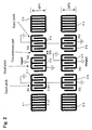
- FIG. 2 shows a surface acousticwave filter constituted of a plurality of sets of the filter structured of a unit shown in FIG. 1 connected in cascade.
- piezoelectric substrate 1 although piezoelectric substrate 1 is not shown, two pairs of reflective electrodes (2-1, 2-2), (2-3, 2-4) are structured on one piezoelectric substrate 1, and three comb electrodes (3-1, 3-2, 3-3), (3-4, 3-5, 3-6) are structured between each pair of the reflective electrodes.
- This structure shown in FIG. 2 also constitutes a multimode filter having a plurality of resonant modes produced by the standing waves.
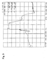
- FIG. 3 shows an example of passband characteristic in such a multimode filter.
- magnitude of attenuation is on the vertical axis, while frequency is on the horizontal axis.
- a range between the frequency in the lower zone and the frequency in the higher zone respectively having the magnitude of attenuation of 3 DB below the minimum attenuation value is referred to as a passband width.
- electrode pitches between the finger electrodes are entirely the same in length, and this is also applicable in comb electrodes 3-4, 3-5, 3-6 in the example shown in FIG. 2.
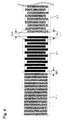
- FIG. 4 there is shown an enlarged diagram of the left portion, halved from the center of the center comb electrode 3-2 in the structure shown in FIG. 1.
- the right portion thereof is obtained by folding the structure shown in FIG. 4 to the right, which is omitted from the figure.
- the lengths of the electrode pitches between the finger electrodes in both comb electrode 3-1 and comb electrode 3-2 are uniform. Further, in FIG. 4, a gap shown as GAP is produced between the outermost finger electrode of comb electrode 3-1 and the outermost finger electrode of comb electrode 3-2.
- GAP gap size
- discontinuity in phase is produced between the phase of a surface acoustic wave SAW1 on comb electrode 3-1 and the phase of a surface acoustic wave SAW2 on comb electrode 3-2.
- FIG. 5 This discontinuity in the phases of the surface acoustic waves is illustrated in FIG. 5, which is observed from the cross sectional direction of piezoelectric substrate 1. As shown in FIG. 5, in the gap shown as GAP, discontinuity is produced between the surface acoustic waves SAW1 and SAW2. This brings about producing a bulk wave radiation 4 passing through piezoelectric substrate 1.
- This bulk wave radiation 4 becomes a major cause of the insertion loss in the surface acoustic wave filter. Therefore, it is necessary to maintain continuity in the phases of the surface acoustic waves.
- the surface acoustic wave filter includes a piezoelectric substrate, a pair of reflective electrodes formed on the piezoelectric substrate; and a plurality of comb electrodes formed between the pair of reflective electrodes on the piezoelectric substrate.
- an electrode pitch of one comb electrode is set so that continuously varying phases of surface acoustic waves respectively generated by the two comb electrodes are obtained in a gap opposite to an outermost finger electrode of the other neighboring comb electrode.
- the surface acoustic wave filter includes a piezoelectric substrate, and a plurality of unit sets of filters formed on the piezoelectric substrate, in which each set is connected to the other in cascade.
- Each plurality pair of filters includes a pair of reflective electrodes, and a plurality of comb electrodes formed between the pair of reflective electrodes on the piezoelectric substrate.
- an electrode pitch of one comb electrode is set so that continuously varying phases of surface acoustic waves respectively generated by the two comb electrodes are obtained in a gap opposite to an outermost finger electrode of the other neighboring comb electrode.
- the surface acoustic wave filter includes a piezoelectric substrate, a pair of reflective electrodes formed on the piezoelectric substrate, and a plurality of comb electrodes formed between the pair of reflective electrodes on the piezoelectric substrate.
- electrode pitches of the respective comb electrodes are set so that continuously varying phases of surface acoustic waves respectively generated by the two comb electrodes are obtained in a gap between outermost finger electrodes of the neighboring two comb electrodes.
- the surface acoustic wave filter includes a piezoelectric substrate, and a plurality of unit sets of filters formed on the piezoelectric substrate, in which each set is connected to the other in cascade.
- Each plurality pair of filters includes a pair of reflective electrodes, and a plurality of comb electrodes formed between the pair of reflective electrodes on the piezoelectric substrate.
- electrode pitches of the respective comb electrodes are set so that continuously varying phases of surface acoustic waves respectively generated by the two comb electrodes are obtained in a gap between outermost finger electrodes of the neighboring two comb electrodes.
- one of the two neighboring comb electrodes is divided into a plurality of blocks, and the electrode pitch is set differently for each divided plurality of blocks.
- each of the two neighboring comb electrodes is divided into a plurality of blocks, and the electrode pitch is set differently for each divided plurality of blocks.
- different electrode pitches are set successively in one of the neighboring two comb electrodes.
- different electrode pitches are set successively in each of the neighboring two comb electrodes.
- the neighboring two comb electrodes are a comb electrode for input and a comb electrode for output, respectively.
- one of the neighboring two comb electrodes disposed in the first stage of the filter set is a comb electrode for input
- one of the neighboring two comb electrodes disposed in the final stage of the filter set is a comb electrode for output.
- the surface acoustic wave filter includes a piezoelectric substrate, a surface acoustic wave resonator formed on the piezoelectric substrate, and a multimode filter which is formed on the piezoelectric substrate and connected in series with the surface acoustic wave resonator.
- the multimode filter includes a pair of reflective electrodes, and a plurality of comb electrodes formed between the pair of reflective electrodes on the piezoelectric substrate.
- an electrode pitch of one comb electrode is set so that continuously varying phases of surface acoustic waves respectively generated by the two comb electrodes are obtained in a gap opposite to an outermost finger electrode of the other neighboring comb electrode.
- the surface acoustic wave filter includes a piezoelectric substrate, a surface acoustic wave resonator formed on the piezoelectric substrate, and a first multimode filter and a second multimode filter each formed on the piezoelectric substrate and connected in series with the surface acoustic wave resonator.
- Each multimode filter includes a pair of reflective electrodes, and a plurality of comb electrodes formed between the pair of reflective electrodes on the piezoelectric substrate.
- an electrode pitch of one comb electrode is set so that continuously varying phases of surface acoustic waves respectively generated by the two comb electrodes are obtained in a gap opposite to an outermost finger electrode of the other neighboring comb electrode.
- a second surface acoustic wave resonator is additionally connected in parallel with the surface acoustic wave resonator.
- the surface acoustic wave resonator is connected to an unbalanced input end or an unbalanced output end, and terminals in the first multimode filter and the second multimode filter are connected to corresponding balanced output ends or balanced input ends.
- FIG. 6 shows a first embodiment of the present invention illustrating a plan view of an electrode structure only, omitting piezoelectric substrate 1 in the same way as FIG. 4.
- the way of above illustration is applied in the following description of other embodiments.
- FIG. 6 there is shown an enlarged view of the left portion halved at the center of the center comb electrode 3-2, in the same way as shown in FIG. 4.
- a leaky surface acoustic wave is used in the surface acoustic wave filter shown in FIG. 6.
- a feature of the embodiment shown in FIG. 6 is that comb electrode 3-1 neighboring comb electrode 3-2 (as for the structure of the right half portion, the above comb electrode 3-1 is to be replaced by comb electrode 3-3) is divided into a plurality of blocks.
- comb electrode 3-1 is divided into three blocks 31, 32 and 33.
- the three blocks 31, 32, 33 are structured with electrode pitches P1, P2, P3, respectively, which are different step-by-step. With this structure, it becomes possible to obtain a continuous phase of the surface acoustic wave in the gap between the outermost finger electrode 321 of comb electrode 3-2 and the outermost finger electrode 322 of comb electrode 3-1.
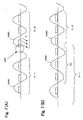
- FIG. 7 (A) is a diagram in which FIG. 5 is repeatedly shown. Discontinuity in phase is being produced between the surface acoustic wave SAW1 on comb electrode 3-1 and the surface acoustic wave SAW2 on comb electrode 3-2.
- FIG. 7 (B) is a diagram according to the embodiment of the present invention, in which the gap opposite to an outermost finger electrode of comb electrode 3-2 is adjusted by the electrode pitch of block 33, that is, one of the plurality of divided blocks in the comb electrode 3-1.
- FIG. 8 shows a second embodiment of the present invention.
- comb electrode 3-1 is so structured as to have different pitches step-by-step, enabling to obtain a continuous wave phase between the finger electrodes in the ends of comb electrodes 3-1, 3-2.
- FIG. 9 shows still another embodiment of the present invention.
- the electrode pitches have been adjusted in comb electrode 3-1, as well as in comb electrode 3-3 in the non-illustrated right portion, to obtain a continuous surface acoustic wave phase between comb electrode 3-1 (3-3) and the neighboring center comb electrode 3-2.
- the electrode pitches in comb electrode 3-2 are also adjusted. This enables easy adjustment of the electrode pitch, as compared to the method of adjusting the pitch in comb electrode 3-1 (3-3) only.
- comb electrode 3-1 is divided into three blocks 31, 32, and 33, having electrode pitches P1, P2 and P3, respectively.
- comb electrode 3-2 is divided into three blocks 21, 22 and 23 (here, block 23 is a block in the non-illustrated right portion of comb electrode 3-2, correspondingly to block 21) .
- the electrode pitches of the three blocks 21, 22, 23 in comb electrode 3-2 are P4, P5, P6, respectively.
- block 23 and the right half of block 22 in comb electrode 3-2 are not shown in FIG. 9.
- the ratios of these electrode pitches P1, P2, P3, P4, P5 are set to satisfy the following relations, assuming the electrode pitch P5 of the center block 22 in comb electrode 3-2 has a reference value '1'.
- P1 0.9976
- P2 0.9669
- P3 0.8986
- P4 0.9375
- P5 1
- FIG. 10 shows a diagram illustrating a passband characteristic of the embodiment shown in FIG. 9 measured against a surface acoustic wave filter which has the electrode pitches P1, P2, P3, P4, P5 set under the relations described above, using the electrode pitch P5 as a reference, and is structured of two stages of cascade connection, as shown in FIG. 2.
- a characteristic A is a passband characteristic of the surface acoustic wave filter according to the present invention
- a characteristic B is a passband characteristic of the conventional surface acoustic wave filter without adjustment of the electrode pitches.
- the passband width I of the surface acoustic wave filter according to the present invention has a wider bandwidth than the passband width II of the conventional surface acoustic wave filter.
- the present invention may be applicable to a surface acoustic wave filter structured of one comb electrode for input and one comb electrode for output, or a surface acoustic wave filter having more than three comb electrodes.
- the filter having the structure shown in FIG. 1 as a filter unit has been shown.
- the present invention may also be applicable to a surface acoustic wave filter structured of two stages, as shown in FIG. 2, or multi-stages more than two stages of a plurality of sets of the filter unit connected in cascade, in which the electrode pitches of the comb filters are adjusted on a filter unit basis.
- the electrode pitches of the center comb electrode 3-2 are fixed, while the electrode pitches of the neighboring comb electrode 3-1 (3-3) are adjusted.
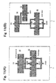
- FIG. 11 shows an exemplary structure of the surface acoustic wave filter, in which the SAW resonator is connected in series to the' multimode filter to obtain a wider bandwidth characteristic with reduced insertion loss in the overall filter.
- the structure shown in FIG. 11 (A) includes a SAW resonator and electrodes constituting a multimode filter 20 on piezoelectric substrate 1, which are connected in series.
- the SAW resonator 10 side constitutes an unbalanced input IN, and an unbalanced output is obtained from multimode filter 20.
- a structure shown in FIG. 11 (B) additionally includes another SAW resonator 11 connected in parallel with SAW resonator 10. With this structure, it is possible to obtain a more preferable filter characteristic.
- FIG. 12 in contrast to the filter structures shown in FIGS. 11 (A) and (B), there is shown a still another structure additionally having a multimode filter 21 connected in parallel with multimode filter 20, though piezoelectric substrate 1 is not shown.
- this structure shown in FIG. 12 it is possible to obtain balanced input or balanced output, which is advantageous in applying to a circuit requiring unbalance-to-balance conversion.
- the present invention is applicable to these multimode filters 20, 21 each having the plurality of comb electrodes (three comb electrodes in FIGS. 11, 12).
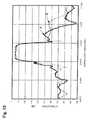
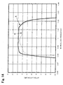
- FIGS. 13, 14 shows diagrams illustrating the characteristic (solid line A) of the surface acoustic wave filter having the structure shown in FIG. 12 (B), in which the present invention is applied to the comb electrodes in each multimode filter 20, 21 to obtain a continuous surface acoustic wave phase between the comb electrode and the reflective electrode, together with diagrams illustrating, for comparison purpose, the characteristic (broken line B) of the conventional surface acoustic wave filter also having the structure shown in FIG. 12 (B), whereas the present invention is not applied in the conventionalsurfaceacoustic wavefilter, and accordingly discontinuity is produced in the surface acoustic wave phases between the comb electrodes and the reflective electrodes.
- FIG. 14 is an enlarged diagram illustrating the passband region in the characteristic diagram shown in FIG. 13.
- the surface acoustic wave filter in accordance with the present invention having the characteristic shown by the solid line A has the dimensions described below.
- multimode filters 20, 21 is structured of
- the numbers of comb electrode pairs of the left reflective electrode and the right reflective electrode are (52), respectively, and further, the numbers of the comb electrode pairs of the three comb electrodes are [(13 - 2 - 1.5) - (2 - 13.5 - 2) - (1.5 - 2 - 13)].
- the electrode pitch of the left reflective electrode is 2.07 ⁇ m
- the electrode pitch of the right reflective electrode is 2. 06 pm
- the electrode pitches of the three comb electrodes are (2.065 - 1.995 - 1.855) - (1.920 - 2.040 - 1.92) -(1.855 - 1.995 - 2.065) ⁇ m.
- the aperture length is 61 ⁇ m.
- SAW resonator 10 connected in series is (reflective electrode - IDT - reflective electrode), and the numbers of the electrode pairs are 50 - 105 - 50 pairs.
- the electrode pitches are 2.007 - 2.007 - 2.007 ⁇ m, and the aperture length is 43 ⁇ m.
- SAW resonator 11 The structure of SAW resonator 11 connected in parallel is (reflective electrode - IDT - reflective electrode), and the numbers of the electrode pairs are 50 - 67 - 50 pairs.
- the electrode pitches are 2.067 - 2.087 - 2.067 ⁇ m, and the aperture length is 55 ⁇ m.
- the conventional surface acoustic wave filter having the characteristic shown by the broken line B has the following dimensions:
- the number of electrode pairs and the electrode pitches of multimode filters 20, 21 are different from the those of the surface acoustic wave filter, in which the present invention is applied, having the characteristic shown by the solid line A.
- the number of electrode pairs of the left reflective electrodes and the number of electrode pairs of the right reflective electrodes are (60) , (40), respectively, and the numbers of the electrode pairs of the three comb electrodes are [(10.5) - (14.5) - (10.5)].
- the electrode pitch of the left reflective electrode is 2.05 ⁇ m
- the electrode pitch of the right reflective electrode is 2.05 ⁇ m
- the electrode pitches of the three comb electrodes are 2.05 - 2.01 - 2.05 ⁇ m
- the aperture length is 60 ⁇ m.
- the design values of the conventional surface acoustic wave filter having the characteristic shown by the broken line B is determined based on a premise of having a predetermined bandwidth. Further, the design values of the surface acoustic wave filter in which the present invention is applied, having the characteristic shown by the solid line A, is also determined based on a premise of having the same bandwidth as the above-mentioned predetermined bandwidth.
- the numbers of the comb electrode pairs in multimode filters 20, 21 in the surface acoustic wave filter in which the present invention is applied having the characteristic shown by the solid line A, are different from corresponding numbers in the conventional surface acoustic wave filter. It is to be understood that the present invention is applicable to a surface acoustic wave filter constituted of the series connection of a SAW resonator and multimode filters, and that the insertion loss can be reduced without damaging the sharp passband characteristic in this surface acoustic wave filter according to the present invention.
Landscapes
- Physics & Mathematics (AREA)
- Acoustics & Sound (AREA)
- Surface Acoustic Wave Elements And Circuit Networks Thereof (AREA)
Abstract
Description
Claims (14)
- A surface acoustic wave filter comprising:wherein, in regard to the neighboring two comb electrodes among the plurality of comb electrodes, an electrode pitch of one comb electrode is set so that continuously varying phases of surface acoustic waves respectively generated by the two comb electrodes are obtained in a gap opposite to an outermost finger electrode of the other neighboring comb electrode.a piezoelectric substrate;a pair of reflective electrodes formed on the piezoelectric substrate; anda plurality of comb electrodes formed between the pair of reflective electrodes on the piezoelectric substrate,
- A surface acoustic wave filter comprising:wherein each plurality of sets of filters includes:a piezoelectric substrate; anda plurality of unit sets of filters formed on the piezoelectric substrate, each set being connected in cascade,a pair of reflective electrodes; anda plurality of comb electrodes formed between the pair of reflective electrodes on the piezoelectric substrate, and,in regard to the neighboring two comb electrodes among the plurality of comb electrodes, an electrode pitch of one comb electrode is set so that continuously varying phases of surface acoustic waves respectively generated by the two comb electrodes are obtained in a gap opposite to an outermost finger electrode of the other neighboring comb electrode.
- A surface acoustic wave filter comprising:wherein, in regard to the neighboring two comb electrodes among the plurality of comb electrodes, electrode pitches of the respective comb electrodes are set so that continuously varying phases of surface acoustic waves respectively generated by the two comb electrodes are obtained in a gap between outermost finger electrodes of the neighboring two comb electrodes.a piezoelectric substrate;a pair of reflective electrodes formed on the piezoelectric substrate; anda plurality of comb electrodes formed between the pair of reflective electrodes on the piezoelectric substrate,
- A surface acoustic wave filter comprising:wherein each plurality of sets of filters includes:a piezoelectric substrate; anda plurality of unit sets of filters formed on the piezoelectric substrate, each set being connected in cascade,a pair of reflective electrodes; anda plurality of comb electrodes formed between the pair of reflective electrodes on the piezoelectric substrate, and,in regard to the neighboring two comb electrodes among the plurality of comb electrodes, electrode pitches of the respective comb electrodes are set so that continuously varying phases of surface acoustic waves respectively generated by the two comb electrodes are obtained in a gap between outermost finger electrodes of the neighboring two comb electrodes.
- The surface acoustic wave filter according to claim 1 or 2,
wherein one of the two neighboring comb electrodes is divided into a plurality of blocks, and the electrode pitch is set differently for each divided plurality of blocks. - The surface acoustic wave filter according to' claim 3 or 4,
wherein each of the two neighboring comb electrodes is divided into a plurality of blocks, and the electrode pitch is set differently for each divided plurality of blocks. - The surface acoustic wave filter according to claim 1 or 2,
wherein different electrode pitches are set successively in one of the neighboring two comb electrodes. - The surface acoustic wave filter according to claim 3 or 4,
wherein different electrode pitches are set successively in each of the neighboring two comb electrodes. - The surface acoustic wave filter according to claim 1 or 3,
wherein the neighboring two comb electrodes are a comb electrode for input and a comb electrode for output, respectively. - The surface acoustic wave filter according to claim 2 or 4,
wherein, among the plurality of sets of filters connected in cascade, one of the neighboring two comb electrodes disposed in the first stage of the filter set is a comb electrode for input, and one of the neighboring two comb electrodes disposed in the final stage of the filter set is a comb electrode for output. - A surface acoustic wave filter comprising:wherein the multimode filter includes:a piezoelectric substrate;a surface acoustic wave resonator formed on the piezoelectric substrate; anda multimode filter which is formed on the piezoelectric substrate and connected in series with the surface acoustic wave resonator,a pair of reflective electrodes; anda plurality of comb electrodes formed between the pair of reflective electrodes on the piezoelectric substrate, and,in regard to the neighboring two comb electrodes among the plurality of comb electrodes, an electrode pitch of one comb electrode is set so that continuously varying phases of surface acoustic waves respectively generated by the two comb electrodes are obtained in a gap opposite to an outermost finger electrode of the other neighboring comb electrode.
- A surface acoustic wave filter comprising:wherein each multimode filter includes:a piezoelectric substrate;a surface acoustic wave resonator formed on the piezoelectric substrate; anda first multimode filter and a second multimode filter each formed on the piezoelectric substrate and connected in series with the surface acoustic wave resonator,a pair of reflective electrodes; anda plurality of comb electrodes formed between the pair of reflective electrodes on the piezoelectric substrate, and,in regard to the neighboring two comb electrodes among the plurality of comb electrodes, an electrode pitch of one comb electrode is set so that continuously varying phases of surface acoustic waves respectively generated by the two comb electrodes are obtained in a gap opposite to an outermost finger electrode of the other neighboring comb electrode.
- The surface acoustic wave filter according to claim 11 or 12,
wherein 'a second surface acoustic wave resonator is additionally connected in parallel with the surface acoustic wave resonator. - The surface acoustic wave filter according to claim 12,
wherein the surface acoustic wave resonator is connected to an unbalanced input end or an unbalanced output end, and terminals in both the first multimode filter and the second multimode filter are connected to corresponding balanced output ends or balanced input ends.
Applications Claiming Priority (5)
| Application Number | Priority Date | Filing Date | Title |
|---|---|---|---|
| JP2001376422 | 2001-12-10 | ||
| JP2001376422 | 2001-12-10 | ||
| JP2002054593 | 2002-02-28 | ||
| JP2002054593A JP4090250B2 (en) | 2001-12-10 | 2002-02-28 | Surface acoustic wave filter |
| PCT/JP2002/009039 WO2003050949A1 (en) | 2001-12-10 | 2002-09-05 | Surface acoustic wave filter |
Publications (3)
| Publication Number | Publication Date |
|---|---|
| EP1453197A1 true EP1453197A1 (en) | 2004-09-01 |
| EP1453197A4 EP1453197A4 (en) | 2007-08-15 |
| EP1453197B1 EP1453197B1 (en) | 2012-08-29 |
Family
ID=26624976
Family Applications (1)
| Application Number | Title | Priority Date | Filing Date |
|---|---|---|---|
| EP02767902A Expired - Lifetime EP1453197B1 (en) | 2001-12-10 | 2002-09-05 | Surface acoustic wave filter |
Country Status (7)
| Country | Link |
|---|---|
| US (2) | US7071796B2 (en) |
| EP (1) | EP1453197B1 (en) |
| JP (1) | JP4090250B2 (en) |
| KR (1) | KR100883247B1 (en) |
| CN (1) | CN100492900C (en) |
| TW (1) | TWI282661B (en) |
| WO (1) | WO2003050949A1 (en) |
Cited By (2)
| Publication number | Priority date | Publication date | Assignee | Title |
|---|---|---|---|---|
| WO2005048457A3 (en) * | 2003-11-12 | 2005-07-14 | Northrop Grumman Corp | Delta-sigma digital-to-analog converter assembly |
| US7102468B2 (en) | 2003-07-02 | 2006-09-05 | Kyocera Corporation | Surface acoustic wave device and communication apparatus using the same |
Families Citing this family (28)
| Publication number | Priority date | Publication date | Assignee | Title |
|---|---|---|---|---|
| DE10345239B4 (en) * | 2003-09-29 | 2013-09-05 | Epcos Ag | With surface waves working transducer |
| JP4622860B2 (en) * | 2004-01-09 | 2011-02-02 | パナソニック株式会社 | Surface acoustic wave filter |
| WO2006004199A1 (en) * | 2004-07-06 | 2006-01-12 | Seiko Epson Corporation | Resonator saw filer |
| WO2006022143A1 (en) | 2004-08-23 | 2006-03-02 | Murata Manufacturing Co., Ltd. | Balanced surface acoustic wave filter |
| US7619347B1 (en) | 2005-05-24 | 2009-11-17 | Rf Micro Devices, Inc. | Layer acoustic wave device and method of making the same |
| JP4688572B2 (en) * | 2005-05-27 | 2011-05-25 | 京セラ株式会社 | Surface acoustic wave resonator, surface acoustic wave device, and communication device |
| JP4583243B2 (en) * | 2005-05-27 | 2010-11-17 | 京セラ株式会社 | Surface acoustic wave resonator, surface acoustic wave device, and communication device |
| JP4646700B2 (en) * | 2005-05-27 | 2011-03-09 | 京セラ株式会社 | Surface acoustic wave resonator, surface acoustic wave device, and communication device |
| JP4698362B2 (en) * | 2005-09-27 | 2011-06-08 | 京セラ株式会社 | Surface acoustic wave resonator, surface acoustic wave device, and communication device |
| TWM299985U (en) * | 2006-02-09 | 2006-10-21 | Yuan High Tech Dev Co Ltd | Audiovisual signal processor with dual antenna |
| JP4741387B2 (en) * | 2006-03-02 | 2011-08-03 | 京セラ株式会社 | Surface acoustic wave resonator, surface acoustic wave device, and communication device |
| JP5094074B2 (en) * | 2006-07-27 | 2012-12-12 | 京セラ株式会社 | Surface acoustic wave device and surface acoustic wave device |
| US8490260B1 (en) | 2007-01-17 | 2013-07-23 | Rf Micro Devices, Inc. | Method of manufacturing SAW device substrates |
| US7408286B1 (en) * | 2007-01-17 | 2008-08-05 | Rf Micro Devices, Inc. | Piezoelectric substrate for a saw device |
| JP2008252678A (en) * | 2007-03-30 | 2008-10-16 | Tdk Corp | Longitudinal coupling resonator type surface acoustic wave filter |
| US8339221B2 (en) | 2008-09-22 | 2012-12-25 | Murata Manufacturing Co., Ltd. | Elastic wave filter device having narrow-pitch electrode finger portions |
| CN102160286B (en) | 2008-09-22 | 2014-03-12 | 株式会社村田制作所 | Elastic wave filter device |
| WO2010035372A1 (en) | 2008-09-24 | 2010-04-01 | 株式会社村田製作所 | Acoustic wave filter device |
| DE102010021164B4 (en) * | 2010-05-21 | 2019-02-21 | Snaptrack, Inc. | Balanced / Unbalanced working SAW filter |
| JP5111586B2 (en) * | 2010-10-04 | 2013-01-09 | 京セラ株式会社 | Surface acoustic wave resonator, surface acoustic wave device, and communication device |
| JP5111585B2 (en) * | 2010-10-04 | 2013-01-09 | 京セラ株式会社 | Surface acoustic wave resonator, surface acoustic wave device, and communication device |
| US8552819B2 (en) * | 2011-10-26 | 2013-10-08 | Triquint Semiconductor, Inc. | High coupling, low loss saw filter and associated method |
| US10389391B2 (en) * | 2016-01-29 | 2019-08-20 | Kyocera Corporation | Acoustic wave resonator, acoustic wave filter, multiplexer, and communication apparatus |
| JP6632481B2 (en) * | 2016-06-22 | 2020-01-22 | 太陽誘電株式会社 | Acoustic wave resonators, filters and multiplexers |
| FR3079101B1 (en) * | 2018-03-16 | 2020-11-06 | Frecnsys | TRANSDUCER STRUCTURE FOR SOURCE SUPPRESSION IN SURFACE ACOUSTIC WAVE FILTER DEVICES |
| US12506462B2 (en) * | 2020-02-28 | 2025-12-23 | Murata Manufacturing Co., Ltd. | Transversely-excited film bulk acoustic resonator with multi-pitch interdigital transducer |
| CN114584104B (en) * | 2022-05-05 | 2022-07-22 | 深圳新声半导体有限公司 | Bulk acoustic wave filter and manufacturing method thereof |
| CN116827296B (en) * | 2023-06-05 | 2024-06-07 | 无锡市好达电子股份有限公司 | Elastic wave filter and preparation method thereof |
Family Cites Families (16)
| Publication number | Priority date | Publication date | Assignee | Title |
|---|---|---|---|---|
| US17969A (en) * | 1857-08-11 | photo-lith o | ||
| EP0115252A3 (en) * | 1982-12-29 | 1985-12-27 | Ciba-Geigy Ag | Mixtures of quaternary polymer ammonium salts, surfactants and fatty acids, their preparation and use in cosmetic compositions |
| JP2620085B2 (en) * | 1987-07-15 | 1997-06-11 | 東洋通信機株式会社 | 2-port SAW resonator |
| JPS6419815U (en) | 1987-07-24 | 1989-01-31 | ||
| JPH09321567A (en) * | 1996-05-28 | 1997-12-12 | Showa Electric Wire & Cable Co Ltd | Resonator saw filter |
| US5986523A (en) * | 1997-08-29 | 1999-11-16 | Murata Manufacturing Co., Ltd. | Edge reflection type longitudinally coupled surface acoustic wave filter |
| US6034586A (en) * | 1998-10-21 | 2000-03-07 | Airpax Corporation, Llc | Parallel contact circuit breaker |
| DE19849782B4 (en) * | 1998-10-28 | 2004-09-30 | Epcos Ag | Surface wave arrangement with at least two surface wave structures |
| US6720842B2 (en) * | 2000-02-14 | 2004-04-13 | Murata Manufacturing Co., Ltd. | Surface acoustic wave filter device having first through third surface acoustic wave filter elements |
| JP2001267885A (en) * | 2000-03-17 | 2001-09-28 | Fujitsu Media Device Kk | Surface acoustic wave device |
| JP3391346B2 (en) | 2000-04-18 | 2003-03-31 | 株式会社村田製作所 | Vertically coupled resonator type surface acoustic wave filter |
| JP3435640B2 (en) * | 2000-05-22 | 2003-08-11 | 株式会社村田製作所 | Vertically coupled resonator type surface acoustic wave filter |
| JP3358615B2 (en) * | 2000-06-26 | 2002-12-24 | 株式会社村田製作所 | Vertically coupled resonator type surface acoustic wave filter |
| US6798318B1 (en) * | 2001-04-27 | 2004-09-28 | Sawtek, Inc. | Hybrid leaky surface acoustic wave resonator filter |
| DE60231043D1 (en) * | 2001-06-29 | 2009-03-19 | Panasonic Corp | SURFACE WAVE FILTER |
| EP1276235A1 (en) * | 2001-07-13 | 2003-01-15 | Matsushita Electric Industrial Co., Ltd. | Surface acoustic wave filter and communication device using the filter |
-
2002
- 2002-02-28 JP JP2002054593A patent/JP4090250B2/en not_active Expired - Lifetime
- 2002-09-05 KR KR1020047008860A patent/KR100883247B1/en not_active Expired - Lifetime
- 2002-09-05 CN CNB028245059A patent/CN100492900C/en not_active Expired - Lifetime
- 2002-09-05 EP EP02767902A patent/EP1453197B1/en not_active Expired - Lifetime
- 2002-09-05 WO PCT/JP2002/009039 patent/WO2003050949A1/en not_active Ceased
- 2002-09-10 TW TW091120598A patent/TWI282661B/en not_active IP Right Cessation
-
2004
- 2004-06-09 US US10/863,484 patent/US7071796B2/en not_active Expired - Lifetime
-
2006
- 2006-04-25 US US11/410,059 patent/US7236067B2/en not_active Expired - Lifetime
Cited By (3)
| Publication number | Priority date | Publication date | Assignee | Title |
|---|---|---|---|---|
| US7102468B2 (en) | 2003-07-02 | 2006-09-05 | Kyocera Corporation | Surface acoustic wave device and communication apparatus using the same |
| WO2005048457A3 (en) * | 2003-11-12 | 2005-07-14 | Northrop Grumman Corp | Delta-sigma digital-to-analog converter assembly |
| US6963297B2 (en) | 2003-11-12 | 2005-11-08 | Northrop Grumman Corporation | Delta-sigma digital-to-analog converter assembly |
Also Published As
| Publication number | Publication date |
|---|---|
| KR100883247B1 (en) | 2009-02-10 |
| JP2003243965A (en) | 2003-08-29 |
| CN1602585A (en) | 2005-03-30 |
| US20040222870A1 (en) | 2004-11-11 |
| US7071796B2 (en) | 2006-07-04 |
| JP4090250B2 (en) | 2008-05-28 |
| WO2003050949A1 (en) | 2003-06-19 |
| CN100492900C (en) | 2009-05-27 |
| KR20040062984A (en) | 2004-07-09 |
| US7236067B2 (en) | 2007-06-26 |
| EP1453197B1 (en) | 2012-08-29 |
| EP1453197A4 (en) | 2007-08-15 |
| US20060192636A1 (en) | 2006-08-31 |
| TWI282661B (en) | 2007-06-11 |
Similar Documents
| Publication | Publication Date | Title |
|---|---|---|
| US7071796B2 (en) | Surface acoustic wave filter | |
| KR100434413B1 (en) | Longitudinally coupled resonator type surface acoustic wave filter | |
| KR100434412B1 (en) | Longitudinally coupled resonator-type surface acoustic wave filter | |
| US6583691B2 (en) | Longitudinally coupled resonator type surface acoustic wave filter with an IDT having a narrow pitch portion | |
| EP0664610B1 (en) | Surface acoustic wave filter | |
| US7646266B2 (en) | Surface acoustic wave resonator and surface acoustic wave filter using the same | |
| US7378923B2 (en) | Balanced SAW filter | |
| US7330089B2 (en) | Balanced acoustic wave filter device | |
| US20020021195A1 (en) | Longitudinally connected resonator type surface acoustic wave filter | |
| KR20010021965A (en) | Surface acoustic wave filter with enhanced edge steepness | |
| US5767603A (en) | Piezoelectric resonators for trap circuits having a plurality of trap frequencies | |
| EP1037385A2 (en) | Surface acoustic wave filter, duplexer, and communications device | |
| KR100874828B1 (en) | Surface acoustic wave filter device | |
| US6965282B2 (en) | Surface acoustic wave device with two split interdigital transducers connected by specified electrode structures | |
| EP1267490A2 (en) | Longitudinally-coupled resonator surface-acoustic wave filter and communications apparatus using the same | |
| EP1251637B1 (en) | Surface acoustic wave apparatus and communication apparatus | |
| EP0980138A1 (en) | Wideband surface wave filter | |
| JP2005203996A (en) | Transversal SAW filter | |
| JP3068035B2 (en) | Surface acoustic wave device | |
| JPH0758581A (en) | Surface acoustic wave resonator filter | |
| JP2000183689A (en) | Vertically coupled dual mode SAW filter |
Legal Events
| Date | Code | Title | Description |
|---|---|---|---|
| PUAI | Public reference made under article 153(3) epc to a published international application that has entered the european phase |
Free format text: ORIGINAL CODE: 0009012 |
|
| 17P | Request for examination filed |
Effective date: 20040603 |
|
| AK | Designated contracting states |
Kind code of ref document: A1 Designated state(s): AT BE BG CH CY CZ DE DK EE ES FI FR GB GR IE IT LI LU MC NL PT SE SK TR |
|
| A4 | Supplementary search report drawn up and despatched |
Effective date: 20070718 |
|
| 17Q | First examination report despatched |
Effective date: 20080528 |
|
| RAP1 | Party data changed (applicant data changed or rights of an application transferred) |
Owner name: TAIYO YUDEN CO., LTD. |
|
| REG | Reference to a national code |
Ref country code: DE Ref legal event code: R079 Ref document number: 60243609 Country of ref document: DE Free format text: PREVIOUS MAIN CLASS: H03H0009145000 Ipc: H03H0009640000 |
|
| GRAP | Despatch of communication of intention to grant a patent |
Free format text: ORIGINAL CODE: EPIDOSNIGR1 |
|
| RIC1 | Information provided on ipc code assigned before grant |
Ipc: H03H 9/64 20060101AFI20120207BHEP Ipc: H03H 9/00 20060101ALI20120207BHEP Ipc: H03H 9/145 20060101ALI20120207BHEP |
|
| GRAS | Grant fee paid |
Free format text: ORIGINAL CODE: EPIDOSNIGR3 |
|
| GRAA | (expected) grant |
Free format text: ORIGINAL CODE: 0009210 |
|
| AK | Designated contracting states |
Kind code of ref document: B1 Designated state(s): DE FI FR GB SE |
|
| REG | Reference to a national code |
Ref country code: GB Ref legal event code: FG4D |
|
| REG | Reference to a national code |
Ref country code: DE Ref legal event code: R096 Ref document number: 60243609 Country of ref document: DE Effective date: 20121025 |
|
| PG25 | Lapsed in a contracting state [announced via postgrant information from national office to epo] |
Ref country code: FI Free format text: LAPSE BECAUSE OF FAILURE TO SUBMIT A TRANSLATION OF THE DESCRIPTION OR TO PAY THE FEE WITHIN THE PRESCRIBED TIME-LIMIT Effective date: 20120829 |
|
| PG25 | Lapsed in a contracting state [announced via postgrant information from national office to epo] |
Ref country code: SE Free format text: LAPSE BECAUSE OF FAILURE TO SUBMIT A TRANSLATION OF THE DESCRIPTION OR TO PAY THE FEE WITHIN THE PRESCRIBED TIME-LIMIT Effective date: 20120829 |
|
| PLBE | No opposition filed within time limit |
Free format text: ORIGINAL CODE: 0009261 |
|
| STAA | Information on the status of an ep patent application or granted ep patent |
Free format text: STATUS: NO OPPOSITION FILED WITHIN TIME LIMIT |
|
| REG | Reference to a national code |
Ref country code: FR Ref legal event code: ST Effective date: 20130628 |
|
| 26N | No opposition filed |
Effective date: 20130530 |
|
| PG25 | Lapsed in a contracting state [announced via postgrant information from national office to epo] |
Ref country code: FR Free format text: LAPSE BECAUSE OF NON-PAYMENT OF DUE FEES Effective date: 20121029 |
|
| REG | Reference to a national code |
Ref country code: DE Ref legal event code: R097 Ref document number: 60243609 Country of ref document: DE Effective date: 20130530 |
|
| REG | Reference to a national code |
Ref country code: DE Ref legal event code: R082 Ref document number: 60243609 Country of ref document: DE Representative=s name: HL KEMPNER PATENTANWALT, RECHTSANWALT, SOLICIT, DE |
|
| PGFP | Annual fee paid to national office [announced via postgrant information from national office to epo] |
Ref country code: DE Payment date: 20210727 Year of fee payment: 20 Ref country code: GB Payment date: 20210728 Year of fee payment: 20 |
|
| REG | Reference to a national code |
Ref country code: DE Ref legal event code: R071 Ref document number: 60243609 Country of ref document: DE |
|
| REG | Reference to a national code |
Ref country code: GB Ref legal event code: PE20 Expiry date: 20220904 |
|
| PG25 | Lapsed in a contracting state [announced via postgrant information from national office to epo] |
Ref country code: GB Free format text: LAPSE BECAUSE OF EXPIRATION OF PROTECTION Effective date: 20220904 |