EP1453113A1 - Piezoelectric element, liquid ejection head and process for manufacturing them - Google Patents
Piezoelectric element, liquid ejection head and process for manufacturing them Download PDFInfo
- Publication number
- EP1453113A1 EP1453113A1 EP03797635A EP03797635A EP1453113A1 EP 1453113 A1 EP1453113 A1 EP 1453113A1 EP 03797635 A EP03797635 A EP 03797635A EP 03797635 A EP03797635 A EP 03797635A EP 1453113 A1 EP1453113 A1 EP 1453113A1
- Authority
- EP
- European Patent Office
- Prior art keywords
- lower electrode
- piezoelectric
- film
- metallic layer
- piezoelectric film
- Prior art date
- Legal status (The legal status is an assumption and is not a legal conclusion. Google has not performed a legal analysis and makes no representation as to the accuracy of the status listed.)
- Withdrawn
Links
Images


Classifications
-
- B—PERFORMING OPERATIONS; TRANSPORTING
- B41—PRINTING; LINING MACHINES; TYPEWRITERS; STAMPS
- B41J—TYPEWRITERS; SELECTIVE PRINTING MECHANISMS, i.e. MECHANISMS PRINTING OTHERWISE THAN FROM A FORME; CORRECTION OF TYPOGRAPHICAL ERRORS
- B41J2/00—Typewriters or selective printing mechanisms characterised by the printing or marking process for which they are designed
- B41J2/005—Typewriters or selective printing mechanisms characterised by the printing or marking process for which they are designed characterised by bringing liquid or particles selectively into contact with a printing material
- B41J2/01—Ink jet
- B41J2/135—Nozzles
- B41J2/14—Structure thereof only for on-demand ink jet heads
- B41J2/14201—Structure of print heads with piezoelectric elements
- B41J2/14233—Structure of print heads with piezoelectric elements of film type, deformed by bending and disposed on a diaphragm
-
- B—PERFORMING OPERATIONS; TRANSPORTING
- B41—PRINTING; LINING MACHINES; TYPEWRITERS; STAMPS
- B41J—TYPEWRITERS; SELECTIVE PRINTING MECHANISMS, i.e. MECHANISMS PRINTING OTHERWISE THAN FROM A FORME; CORRECTION OF TYPOGRAPHICAL ERRORS
- B41J2/00—Typewriters or selective printing mechanisms characterised by the printing or marking process for which they are designed
- B41J2/005—Typewriters or selective printing mechanisms characterised by the printing or marking process for which they are designed characterised by bringing liquid or particles selectively into contact with a printing material
- B41J2/01—Ink jet
- B41J2/135—Nozzles
- B41J2/16—Production of nozzles
- B41J2/1607—Production of print heads with piezoelectric elements
- B41J2/161—Production of print heads with piezoelectric elements of film type, deformed by bending and disposed on a diaphragm
-
- B—PERFORMING OPERATIONS; TRANSPORTING
- B41—PRINTING; LINING MACHINES; TYPEWRITERS; STAMPS
- B41J—TYPEWRITERS; SELECTIVE PRINTING MECHANISMS, i.e. MECHANISMS PRINTING OTHERWISE THAN FROM A FORME; CORRECTION OF TYPOGRAPHICAL ERRORS
- B41J2/00—Typewriters or selective printing mechanisms characterised by the printing or marking process for which they are designed
- B41J2/005—Typewriters or selective printing mechanisms characterised by the printing or marking process for which they are designed characterised by bringing liquid or particles selectively into contact with a printing material
- B41J2/01—Ink jet
- B41J2/135—Nozzles
- B41J2/16—Production of nozzles
- B41J2/1621—Manufacturing processes
- B41J2/1623—Manufacturing processes bonding and adhesion
-
- B—PERFORMING OPERATIONS; TRANSPORTING
- B41—PRINTING; LINING MACHINES; TYPEWRITERS; STAMPS
- B41J—TYPEWRITERS; SELECTIVE PRINTING MECHANISMS, i.e. MECHANISMS PRINTING OTHERWISE THAN FROM A FORME; CORRECTION OF TYPOGRAPHICAL ERRORS
- B41J2/00—Typewriters or selective printing mechanisms characterised by the printing or marking process for which they are designed
- B41J2/005—Typewriters or selective printing mechanisms characterised by the printing or marking process for which they are designed characterised by bringing liquid or particles selectively into contact with a printing material
- B41J2/01—Ink jet
- B41J2/135—Nozzles
- B41J2/16—Production of nozzles
- B41J2/1621—Manufacturing processes
- B41J2/1626—Manufacturing processes etching
- B41J2/1628—Manufacturing processes etching dry etching
-
- B—PERFORMING OPERATIONS; TRANSPORTING
- B41—PRINTING; LINING MACHINES; TYPEWRITERS; STAMPS
- B41J—TYPEWRITERS; SELECTIVE PRINTING MECHANISMS, i.e. MECHANISMS PRINTING OTHERWISE THAN FROM A FORME; CORRECTION OF TYPOGRAPHICAL ERRORS
- B41J2/00—Typewriters or selective printing mechanisms characterised by the printing or marking process for which they are designed
- B41J2/005—Typewriters or selective printing mechanisms characterised by the printing or marking process for which they are designed characterised by bringing liquid or particles selectively into contact with a printing material
- B41J2/01—Ink jet
- B41J2/135—Nozzles
- B41J2/16—Production of nozzles
- B41J2/1621—Manufacturing processes
- B41J2/1631—Manufacturing processes photolithography
-
- B—PERFORMING OPERATIONS; TRANSPORTING
- B41—PRINTING; LINING MACHINES; TYPEWRITERS; STAMPS
- B41J—TYPEWRITERS; SELECTIVE PRINTING MECHANISMS, i.e. MECHANISMS PRINTING OTHERWISE THAN FROM A FORME; CORRECTION OF TYPOGRAPHICAL ERRORS
- B41J2/00—Typewriters or selective printing mechanisms characterised by the printing or marking process for which they are designed
- B41J2/005—Typewriters or selective printing mechanisms characterised by the printing or marking process for which they are designed characterised by bringing liquid or particles selectively into contact with a printing material
- B41J2/01—Ink jet
- B41J2/135—Nozzles
- B41J2/16—Production of nozzles
- B41J2/1621—Manufacturing processes
- B41J2/164—Manufacturing processes thin film formation
- B41J2/1642—Manufacturing processes thin film formation thin film formation by CVD [chemical vapor deposition]
-
- B—PERFORMING OPERATIONS; TRANSPORTING
- B41—PRINTING; LINING MACHINES; TYPEWRITERS; STAMPS
- B41J—TYPEWRITERS; SELECTIVE PRINTING MECHANISMS, i.e. MECHANISMS PRINTING OTHERWISE THAN FROM A FORME; CORRECTION OF TYPOGRAPHICAL ERRORS
- B41J2/00—Typewriters or selective printing mechanisms characterised by the printing or marking process for which they are designed
- B41J2/005—Typewriters or selective printing mechanisms characterised by the printing or marking process for which they are designed characterised by bringing liquid or particles selectively into contact with a printing material
- B41J2/01—Ink jet
- B41J2/135—Nozzles
- B41J2/16—Production of nozzles
- B41J2/1621—Manufacturing processes
- B41J2/164—Manufacturing processes thin film formation
- B41J2/1646—Manufacturing processes thin film formation thin film formation by sputtering
-
- H—ELECTRICITY
- H10—SEMICONDUCTOR DEVICES; ELECTRIC SOLID-STATE DEVICES NOT OTHERWISE PROVIDED FOR
- H10N—ELECTRIC SOLID-STATE DEVICES NOT OTHERWISE PROVIDED FOR
- H10N30/00—Piezoelectric or electrostrictive devices
- H10N30/01—Manufacture or treatment
- H10N30/07—Forming of piezoelectric or electrostrictive parts or bodies on an electrical element or another base
- H10N30/074—Forming of piezoelectric or electrostrictive parts or bodies on an electrical element or another base by depositing piezoelectric or electrostrictive layers, e.g. aerosol or screen printing
- H10N30/077—Forming of piezoelectric or electrostrictive parts or bodies on an electrical element or another base by depositing piezoelectric or electrostrictive layers, e.g. aerosol or screen printing by liquid phase deposition
- H10N30/078—Forming of piezoelectric or electrostrictive parts or bodies on an electrical element or another base by depositing piezoelectric or electrostrictive layers, e.g. aerosol or screen printing by liquid phase deposition by sol-gel deposition
-
- H—ELECTRICITY
- H10—SEMICONDUCTOR DEVICES; ELECTRIC SOLID-STATE DEVICES NOT OTHERWISE PROVIDED FOR
- H10N—ELECTRIC SOLID-STATE DEVICES NOT OTHERWISE PROVIDED FOR
- H10N30/00—Piezoelectric or electrostrictive devices
- H10N30/20—Piezoelectric or electrostrictive devices with electrical input and mechanical output, e.g. functioning as actuators or vibrators
- H10N30/204—Piezoelectric or electrostrictive devices with electrical input and mechanical output, e.g. functioning as actuators or vibrators using bending displacement, e.g. unimorph, bimorph or multimorph cantilever or membrane benders
- H10N30/2047—Membrane type
-
- B—PERFORMING OPERATIONS; TRANSPORTING
- B41—PRINTING; LINING MACHINES; TYPEWRITERS; STAMPS
- B41J—TYPEWRITERS; SELECTIVE PRINTING MECHANISMS, i.e. MECHANISMS PRINTING OTHERWISE THAN FROM A FORME; CORRECTION OF TYPOGRAPHICAL ERRORS
- B41J2/00—Typewriters or selective printing mechanisms characterised by the printing or marking process for which they are designed
- B41J2/005—Typewriters or selective printing mechanisms characterised by the printing or marking process for which they are designed characterised by bringing liquid or particles selectively into contact with a printing material
- B41J2/01—Ink jet
- B41J2/135—Nozzles
- B41J2/14—Structure thereof only for on-demand ink jet heads
- B41J2/14201—Structure of print heads with piezoelectric elements
- B41J2/14233—Structure of print heads with piezoelectric elements of film type, deformed by bending and disposed on a diaphragm
- B41J2002/14258—Multi layer thin film type piezoelectric element
-
- B—PERFORMING OPERATIONS; TRANSPORTING
- B41—PRINTING; LINING MACHINES; TYPEWRITERS; STAMPS
- B41J—TYPEWRITERS; SELECTIVE PRINTING MECHANISMS, i.e. MECHANISMS PRINTING OTHERWISE THAN FROM A FORME; CORRECTION OF TYPOGRAPHICAL ERRORS
- B41J2/00—Typewriters or selective printing mechanisms characterised by the printing or marking process for which they are designed
- B41J2/005—Typewriters or selective printing mechanisms characterised by the printing or marking process for which they are designed characterised by bringing liquid or particles selectively into contact with a printing material
- B41J2/01—Ink jet
- B41J2/135—Nozzles
- B41J2/14—Structure thereof only for on-demand ink jet heads
- B41J2002/14491—Electrical connection
-
- H—ELECTRICITY
- H10—SEMICONDUCTOR DEVICES; ELECTRIC SOLID-STATE DEVICES NOT OTHERWISE PROVIDED FOR
- H10N—ELECTRIC SOLID-STATE DEVICES NOT OTHERWISE PROVIDED FOR
- H10N30/00—Piezoelectric or electrostrictive devices
- H10N30/80—Constructional details
- H10N30/85—Piezoelectric or electrostrictive active materials
- H10N30/853—Ceramic compositions
- H10N30/8548—Lead-based oxides
- H10N30/8554—Lead-zirconium titanate [PZT] based
Definitions
- the present invention relates to a piezoelectric element having an electromechanical conversion function, a liquid discharge head using this piezoelectric element and a method of manufacturing these.
- a piezoelectric element whereby excellent voltage withstanding ability and durability are obtained, a liquid discharge head using this and a method of manufacturing these.
- a liquid discharge head such as an inkjet recording head employs a piezoelectric element as a drive source for discharge of a liquid droplet such as an ink droplet.
- a piezoelectric element comprises a piezoelectric thin film and an upper electrode and a lower electrode arranged sandwiching this piezoelectric thin film.
- Laid-open Japanese Patent Application No. 2000-198197 discloses forming the piezoelectric thin film after patterning of the lower electrode in a prescribed shape.
- An object of the present invention is to provide a piezoelectric element and liquid discharge head of higher reliability and capable of withstanding high voltage, by securing excellent crystallinity of the piezoelectric film in the vicinity of the edges of the lower electrode.
- a piezoelectric element comprises a diaphragm, a lower electrode formed with a prescribed pattern on the diaphragm, a piezoelectric film formed on the lower electrode and an upper electrode formed on the piezoelectric film. Also, in the vicinity of the piezoelectric film, there is provided a metallic layer formed on the diaphragm and constituting a metallic layer which is electrically disconnected from the lower electrode. By providing a metallic layer in the vicinity of the region where the piezoelectric film is formed, baking conditions of the piezoelectric film can be made uniform and excellent crystallinity of the piezoelectric film can be achieved, even in the vicinity of the edges of the lower electrode.
- the metallic layer is formed of the same material as the lower electrode. Also, preferably the gap between the lower electrode and the metallic layer which is electrically disconnected there from is no more than 200 ⁇ m.
- the piezoelectric film is formed so as to at least partially cover the aforesaid metallic layer and an electrode that extends from the upper electrode and is provided for wiring purposes is formed on a portion of the aforesaid metallic layer which is covered by the piezoelectric film, being insulated from the metallic layer by this piezoelectric film.
- a second metallic layer constituting a metallic layer formed on the diaphragm and electrically connected with the electrode for wiring purposes that extends from the upper electrode but electrically disconnected from the lower electrode.
- the piezoelectric film is formed on the lower electrode, which is formed in the prescribed pattern, and on the diaphragm where the lower electrode is not present, and in the portion of the piezoelectric film that is formed on the lower electrode the number of layers of the aforesaid piezoelectric film is larger than in the portion formed on the diaphragm.
- a liquid discharge head comprises a piezoelectric element as above, a pressure chamber whose internal volume is changed by mechanical displacement of this piezoelectric element, and a discharge port whereby a liquid droplet is discharged, communicating with this pressure chamber.
- a liquid discharge device comprises a liquid discharge head as described above and a drive device that drives this liquid discharge head.
- a method of manufacturing a piezoelectric element according to the present invention comprises the step of forming a lower electrode and a metallic layer in the vicinity of the lower electrode on a diaphragm in a prescribed pattern; the step of forming a piezoelectric film on the lower electrode; and the step of forming an upper electrode on the piezoelectric film; the metallic layer being formed so as to be electrically disconnected from the lower electrode.
- Another method of manufacturing a piezoelectric element comprises the step of depositing a conductive film on a diaphragm; a first step of depositing a piezoelectric film in which a piezoelectric film is deposited on the conductive film; the step of dividing the conductive film into a lower electrode and a metallic layer that is positioned in the vicinity of the lower electrode and electrically disconnected from this lower electrode, by patterning of the conductive film and the piezoelectric film deposited in the first piezoelectric film deposition step; a second piezoelectric film deposition step of depositing a further piezoelectric film on the piezoelectric film left by the patterning and on the diaphragm where the piezoelectric film was removed; and the step of forming an upper electrode on the piezoelectric film.
- a method of manufacturing a liquid discharge head comprises the step of forming a piezoelectric element by the above method; the step of forming a pressure chamber whose internal volume is changed by mechanical displacement of the piezoelectric element; and the step of forming a discharge port whereby a liquid droplet is discharged, communicating with this pressure chamber.
- reference symbol 20 indicates a pressure chamber substrate
- 30 indicates a diaphragm
- 31 indicates an oxide film
- 32 indicates a ZrO 2 film
- 40 indicates a piezoelectric element
- 42 indicates a conductive layer
- 42a indicates an inside metallic layer
- 42b indicates an outside metallic layer
- 42d indicates a lower electrode
- 43 indicates a piezoelectric thin film
- 44 indicates an upper electrode.
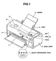
- FIG. 1 is a perspective view showing the construction of a printer constituting a liquid discharge device wherein a piezoelectric element according to an embodiment of the present invention is employed.
- the main body 2 is provided with a tray 3, a discharge port 4 and control buttons 9.
- an inkjet recording head 1 constituting a liquid discharge head, a paper feed mechanism 6 and a control circuit 8.
- the inkjet recording head 1 comprises a plurality of piezoelectric elements formed on a substrate and is constituted so as to be capable of discharging ink constituting the liquid from a nozzle in response to a discharge signal supplied from the control circuit 8.
- the main body 2 constitutes a printer casing, with a paper feed mechanism 6 arranged in a position capable of being supplied with paper 5 from a tray 3 and an inkjet recording head 1 capable of printing onto the paper 5.
- the tray 3 is constituted so as to be capable of supplying blank paper 5 to the paper feed mechanism 6 and the discharge port 4 constitutes a discharge port whereby paper 5 is discharged after printing.
- the paper feed mechanism 6 comprises a motor 600, rollers 601, 602 and other mechanical structures, not shown.
- the motor 600 is rotatable in response to a drive signal supplied from the control circuit 8.
- the mechanical structures are constituted so as to be capable of transmitting the rotational force of the motor 600 to the rollers 601 and 602.
- the rollers 601 and 602 are arranged to be rotated when rotational force of the motor 600 is transmitted thereto, so as to entrain paper 5 placed in the tray 3 by their rotation and to feed this paper so that it can be printed by the head 1.
- the control circuit 8 comprises a CPU, ROM and RAM, and an interface circuit, not shown, and is arranged to supply drive signals to the paper feed mechanism 6 in response to printing information supplied from the computer through a connector, not shown, or to supply a discharge signal to the inkjet recording head 1. Also, the control circuit 8 is arranged to be capable of performing processing such as setting or resetting of the operating mode in response to control signals from the control panel 9.
- the printer of this embodiment is a high-performance printer, being provided with an inkjet recording head having excellent voltage withstanding ability and durability and excellent printing performance as will be described.
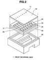
- Figure 2 is an exploded perspective view showing the construction of major parts of an inkjet recording head constituting a liquid discharge head according to an embodiment of the present invention.
- the inkjet recording head comprises a nozzle plate 10, pressure chamber substrate 20 and diaphragm 30.
- the pressure chamber substrate 20 comprises pressure chambers (cavities) 21, side walls 22, a reservoir 23 and supply ports 24.
- the pressure chambers 21 constitutes spaces for accumulating for example ink for discharge and are formed by etching a substrate made for example of silicon.
- the side walls 22 are formed so as to partition the pressure chambers 21.
- the reservoir 23 constitutes a common flow path for supply of ink through the supply port 24 to the respective pressure chambers 21.
- the nozzle plate 10 is stuck onto one face of the pressure chamber substrate 20 such that nozzles 11 thereof are arranged in positions respectively corresponding to the pressure chambers 21 provided in the pressure chamber substrate 20.
- the diaphragm 30 is formed by laminating an oxide film 31 and ZrO 2 film 32, as will be described, and is stuck onto the other face of the pressure chamber substrate 20.
- the diaphragm 30 is provided with an inkjet connection port, not shown, so as to be capable of supplying ink accumulated in an ink tank, not shown, to the reservoir 23 of the pressure chamber substrate 20.
- the inkjet recording head 1 is constituted by a head unit comprising the nozzle plate 10, diaphragm 30 and pressure chamber substrate 20 and is accommodated in the casing 25.
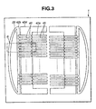
- Figure 3 is a plan view showing details of the arrangement of piezoelectric elements in the inkjet recording head of the first embodiment.
- a large number of piezoelectric elements 40 are arranged alternately in two rows.
- 360 piezoelectric elements 40 are arranged in one inch in the first row and in the second row 360 piezoelectric elements 40 are arranged in positions offset by 1/720 inch with respect to the first row.
- the lower electrodes 42d of the piezoelectric elements 40 are electrodes that are common to each row.
- an outside metallic layer 42b that is electrically disconnected from the lower electrode 42d and from the upper electrodes 44, to be described.
- the inside metallic layer 42a and outside metallic layer 42b that are here referred to surround the portions of the lower electrode 42d where piezoelectric elements 40 are not formed and also the piezoelectric elements 40.
- Narrow strip electrodes 45 for respective wiring extend from the upper electrodes of the piezoelectric elements 40 to the inside of each row, passing above the inside metallic layer 42a without contacting the inside metallic layer 42a.
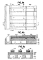
- Figure 4 shows a plan view (a) to a larger scale of the portion enclosed by the line iii in Figure 3, a cross-sectional view (b) along the line i-i thereof and a cross-sectional view (c) along the line ii-ii.
- the respective individual discharge sections of the inkjet head 1 are constituted by successively laminating ZrO 2 film 32, lower electrode 42d, piezoelectric thin film 43 and upper electrodes 44 on an oxide film 31.
- the oxide film 31 is formed as an insulating film on the pressure chamber substrate 20 made of monocrystalline silicon of for example thickness 100 ⁇ m.
- a film made of silicon oxide (SiO 2 ) may be formed in a thickness of 1.0 ⁇ m.
- the ZrO 2 film 32 is a layer providing resilience and is used, integrated with the oxide film 31, to constitute the diaphragm 30. Since this ZrO 2 film 32 provides the function of conferring resilience, it preferably has a thickness of at least 200 nm and less than 800 nm.
- An adhesion layer (not shown) made of metal, preferably titanium or chromium, may be provided between the ZrO 2 film 32 and the lower electrode 42d so as to stick these two layers together.
- the adhesion layer is a layer formed to improve adhesion to the surface where the piezoelectric elements are arranged and need not be formed if such adhesion can be guaranteed. Also, if such an adhesion layer is provided, it is preferably of a thickness of at least 10 nm.
- the lower electrode 42d is in this case of a layered construction of layers containing at least Ir, for example, from the lowest layer, a layer containing Ir, a layer containing Pt, and a layer containing Ir.
- the overall thickness of the lower electrode 42d may be for example 200 nm.
- the layered construction of the lower electrode 42d is not restricted to this and could be a double-layered construction of a layer containing Ir and a layer containing Pt or a layer containing Pt and a layer containing Ir. It could also be constituted solely by a layer containing Ir.
- the piezoelectric thin film 43 consists of a ferroelectric body constituted by crystals of piezoelectric ceramics and is preferably a ferroelectric piezoelectric material such as lead zirconate titanate (PZT) or a material obtained by adding a metallic oxide such as niobium oxide, nickel oxide or magnesium oxide thereto.
- the composition of the piezoelectric thin film 43 is suitably selected taking into account for example the performance and application of the piezoelectric element.
- films of excellent piezoelectric characteristics may be obtained by suitable addition of niobium (Nb) to lead titanate and/or lead zirconate.
- the thickness of the piezoelectric thin film 43 is kept sufficiently low that cracks are not produced in the manufacturing step but, on the other hand, must be thick enough to achieve sufficient displacement performance: for example at least 1000 nm but not more than 1500 nm is suitable.
- the upper electrodes 44 are electrodes paired with the lower electrode 42d and are preferably constructed of Pt or Ir.
- the thickness of the upper electrodes 44 is preferably about 50 nm.
- the lower electrode 42d is an electrode that is common to the respective piezoelectric elements.
- the inside metallic layer 42a and outside metallic layer 42b are positioned on a layer that is of the same height as the lower electrode 42d, but are isolated from the lower electrode 42d.
- the separation between these is 200 ⁇ m or less, preferably 100 ⁇ m or less and even more preferably 50 ⁇ m or less.
- the lower limit of the separation may be a separation such as to produce an electrically non-conductive condition: for example a separation of at least 5 ⁇ m is desirable.
- the piezoelectric thin films 43 of the individual piezoelectric elements 40 extend above the inside metallic layer 42a and conductive narrow strip electrodes 45 for wiring purposes are formed thereon on the upper electrodes 44.
- the narrow strip electrodes 45 are insulated from the inside metallic layer 42a by the piezoelectric thin films 43.
- the inside metallic layer 42a is formed of the same material as the lower electrode 42d. Even if the inside metallic layer 42a is not formed of the same material, it should preferably have an infra-red absorptivity approximating to the material of the lower electrode 42d.
- the outside metallic layer 42b is also positioned on a layer of the same height as the lower electrode 42d, but is isolated from the lower electrode 42d and the inside metallic layer 42a.
- the separation thereof is 200 ⁇ m or less, preferably 100 ⁇ m or less and even more preferably 50 ⁇ m or less.
- the lower limit of the separation may be a separation such as to produce an electrically non-conductive condition: for example a separation of at least 5 ⁇ m is desirable.
- the outside metallic layer 42b is isolated from the narrow strip electrodes 45 and the upper electrodes 44. Also, although the piezoelectric thin film 43 is formed partially on the outside metallic layer 42b, the upper electrodes 44 and the outside metallic layer 42b are in non-contacting condition.
- the outside metallic layer 42b is formed of the same material as the lower electrode 42d. Even if the outside metallic layer 42b is not formed of the same material, it should preferably have an infra-red absorptivity approximating to the material of the lower electrode 42d.
- a reservoir 23 for supplying liquid to the pressure chambers 21 is provided in a position closer to the outside metallic layer 42b than the piezoelectric elements 40.
- Figure 5 is a plan view showing details of the arrangement of piezoelectric elements in an inkjet recording head according to a second embodiment. Parts having the same function as in the first embodiment are given the same reference symbols.
- the second metallic layer constituted by an inside metallic layer 42c is divided into segments corresponding to the piezoelectric elements 40. Narrow strip electrodes 45 are formed directly above the respective segments of the inside metallic layer 42c, so the inside metallic layer 42c cannot be seen in plan view in Figure 5.
- Figure 6 shows a plan view (a) to a larger scale of the portion enclosed by the line iii in Figure 5, a cross-sectional view (b) along the line i-i thereof and a cross-sectional view (c) along the line ii-ii.
- the piezoelectric film 43 does not completely cover the inside metallic layer 42c.
- the narrow strip electrodes 45 for wiring that are electrically connected with the upper electrodes 44 are capable of connection with the inside metallic layer 42c.
- the inside metallic layer 42c is not connected with the lower electrode 42d, and adjacent segments of the inside electrode layer 42c are not connected, so even if connection occurs with the narrow strip electrodes 45, this causes no electrical problems.
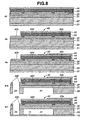
- Figure 7 and Figure 8 are cross-sectional diagrams showing this piezoelectric element and a method of manufacturing an inkjet recording head.
- the description with reference to Figure 7 and Figure 8 follows the construction of the inkjet recording head of the first embodiment described with reference to Figure 3 and Figure 4 above; however, an inkjet recording head according to the second embodiment described in Figure 5 and Figure 6 can also be manufactured by the same procedure as this.
- This step is a step in which an oxide film 31 made of silicon oxide (SiO 2 ) is formed by high-temperature treatment of the silicon substrate constituting the pressure chamber substrate 20 in an oxidizing atmosphere containing oxygen or water vapor.
- a CVD method could also be employed.
- This step is a step of forming a ZrO 2 film 32 on the oxide film 31 formed on one face of the pressure chamber substrate 20.
- This ZrO 2 film 32 is obtained by high-temperature processing in an oxidizing atmosphere after forming a Zr layer by for example a sputtering method or vacuum evaporation method.
- a conductive film 42 containing Ir and constituting the lower electrode is formed on the ZrO 2 film 32. For example, first of all, a layer containing Ir is formed, then a layer containing Pt is formed and, in addition, a further layer containing Ir is formed.
- the layers constituting the conductive film 42 are formed by depositing using for example the sputtering method, respectively Ir or Pt on the ZrO 2 film 32.
- an adhesion layer (not shown) made of titanium or chromium may be formed by the sputtering method or vacuum evaporation method.
- patterning is performed by first of all masking the conductive film 42 to the desired shape and then etching the periphery thereof, in order to divide this conductive film into an inside metallic layer 42a and outside metallic layer 42b and lower electrode 42d.
- resist material of uniform thickness is applied (not shown) onto the conductive layer 42 by a method such as the spinner method or spray method; next, a mask is formed to the shape of the piezoelectric elements and exposure and development are performed to form a resist pattern on the conductive film (not shown).
- Part of the conductive film is removed by etching using for example the ion milling or dry etching method which are normally employed and the ZrO 2 film 32 is exposed, to form an inside metallic layer 42a, outside metallic layer 42b and lower electrode 42d.
- This step is a step in which Ti nuclei (layer) (not shown) are formed on the lower electrode 42d by for example the sputtering method.
- the reason for forming the Ti nuclei (layer) is that crystal growth then takes place from the side of the lower electrode, enabling fine pillar-shaped crystals to be obtained by growing PZT using the Ti crystals as nuclei.
- the mean thickness of the Ti nuclei (layer) is 3 to 7 nm, preferably 4 to 6 nm.
- This step is a step of forming a piezoelectric precursor film 43' by the sol gel method.
- a sol made of a solution of organic metallic alkoxide is applied onto the Ti nuclei by a method of application such as for example spin coating.
- drying is performed for a fixed period at a fixed temperature to evaporate the solvent.
- degreasing is performed for a fixed time at a prescribed high temperature under ordinary atmosphere, to pyrolyse organic ligands that are coordinated with the metal and create metallic oxide.
- a piezoelectric precursor film consisting of two layers is laminated by repeating a prescribed number of times, for example twice, these steps of application, drying and degreasing.
- this step is not restricted to the sol gel method but could also be performed by the MOD (metal organic deposition) method.
- the piezoelectric thin film 43' is made to change from an amorphous condition to a rhombohedral crystalline structure, changing to a thin film showing an electromechanical conversion effect, thereby becoming a piezoelectric thin film 43.
- the ZrO 2 film 32 has a lower absorptivity for near infra-red rays than the lower electrode 42d, the rise in temperature during baking is slowed in regions where the lower electrode 42d is not formed.
- the regions where the piezoelectric film is formed are surrounded by the lower electrode 42d, inside metallic layer 42a and outside metallic layer 42b, so a sufficient temperature rise can still be ensured even in the regions where the lower electrode 42d is not formed.
- uniform baking conditions of the piezoelectric thin film are achieved.
- crystallinity of the piezoelectric thin film in particular in the vicinity of the edges of the lower electrode 42d is improved, improving voltage withstanding ability and durability.
- the baking conditions can be made uniform in the entire wafer, uniform voltage characteristics among the piezoelectric elements can be achieved.
- a piezoelectric thin film 43 of the desired thickness can be produced by repeating the above formation of a precursor film (S5) and baking thereof (S6) a plurality of times. If for example the film thickness of the precursor film applied for a single baking is taken as 200 nm, this would be repeated six times.
- Upper electrodes 44 are formed on the piezoelectric thin film 43 by an electron beam evaporation method or sputtering method.
- narrow strip electrodes 45 are formed connected with the upper electrodes 44.
- the narrow strip electrodes 45 are preferably made of gold, which is a material of low rigidity and low electrical resistance. Apart from this, for example aluminum or copper are suitable.
- the narrow strip electrodes 45 are produced by depositing a film of thickness about 0.5 ⁇ m, followed by patterning to produce wiring effecting connection with the upper electrodes.
- the pressure chambers 21, reservoir 23 and supply port 24 are formed by performing anisotropic etching on the other face of the pressure chamber substrate 20 that is formed with the piezoelectric elements 40, or anisotropic etching using a reactive gas such as in parallel plate type reactive ion etching.
- the portions that are left behind without being etched constitute the side walls 22.
- the reservoir 23 is formed in a shape rather smaller than the outside metallic layer 42b in a position facing the outside metallic layer 42b and is formed with through-holes using for example a laser.
- a nozzle plate 10 is stuck on using adhesive.
- positional alignment is effected such that the nozzles 11 are arranged at the spaces of the respective pressure chambers 21.
- the pressure chamber substrate 20 is mounted in a casing, not shown, thereby completing the inkjet recording head 1.
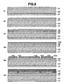
- FIG. 9 is a cross-sectional diagram showing a modified example of the above method of manufacture and shows a step corresponding to Figure 7.
- Steps S1 to S3 are the same as in the case of Figure 7 and the steps after S6c are the same as in the case of Figure 8, so further description thereof will be dispensed with.
- a conductive film 42 has been formed in S3
- a first layer 43a of piezoelectric thin film is formed (S6a) prior to patterning and thereafter patterning is performed (S6b) combining the first layer 43a of piezoelectric thin film and the conductive layer 42.
- a first layer 43a of piezoelectric thin film is formed on the conductive film 42.
- the method of forming consists in for example forming Ti nuclei (layer) in a thickness of 3 to 7 nm, preferably 4 to 6 nm, and then, as described in S5 and S6 of Figure 7 above, repeating the steps of sol application, drying and degreasing twice, followed by baking, to form a first layer 43a of piezoelectric thin film of about 200 nm.
- the first layer 43a of the piezoelectric thin film and the conductive film 42 are patterned to the same shape as in S4 of Figure 7.
- the conductive film 42a is separated into the lower electrode 42d, inside metallic layer 42a and outside metallic layer 42b.
- the ZrO 2 film 32 is exposed in the portions where the first layer 43a of piezoelectric thin film and the conductive film 42 are removed.
- a piezoelectric thin film 43 of more layers than on the above exposed ZrO 2 film 32 is formed on the lower electrode 42d.
- a piezoelectric thin film 43 of six layers may be formed on the lower electrode 42d and a piezoelectric thin film of 43 of five layers may be formed on the exposed ZrO 2 film 32.
- the inkjet recording head according to the above embodiment had a voltage withstanding ability of 90 to 110 V (the locations where cracking occurred were random, not being concentrated in a specific portion).
- Durability was investigated using a drive voltage of 35 V. Whereas the conventional inkjet recording head showed a deterioration of performance after about 1 billion pulses, in the case of the present embodiment, the inkjet recording head was able to withstand drive with at least 40 billion pulses. It was therefore concluded that an inkjet recording head according to this embodiment showed an outstanding improvement in performance.
- piezoelectric elements manufactured in accordance with the present invention can be applied not merely to the piezoelectric elements of an inkjet recording head as described above but also to the manufacture of non-volatile semiconductor memory devices, thin film capacitors, pyroelectric detectors, sensors, SAW optical waveguides, optical memory devices, spatial light modulators, ferroelectric devices such as frequency doublers for diode lasers, dielectric devices, pyroelectric devices, piezoelectric devices and electro optical devices.
- a liquid discharge head according to the present invention can be applied to various types of head that spray liquid such as for example heads that discharge liquid containing a pigment employed in the manufacture of color filters for for example liquid-crystal displays, heads that discharge liquid containing electrode material employed in the formation of electrodes such as organic EL displays or FED (face emission displays), or heads that discharge liquid containing bio-organic substances employed in biochip manufacture.
- head that spray liquid such as for example heads that discharge liquid containing a pigment employed in the manufacture of color filters for for example liquid-crystal displays, heads that discharge liquid containing electrode material employed in the formation of electrodes such as organic EL displays or FED (face emission displays), or heads that discharge liquid containing bio-organic substances employed in biochip manufacture.
Landscapes
- Engineering & Computer Science (AREA)
- Manufacturing & Machinery (AREA)
- Chemical & Material Sciences (AREA)
- Dispersion Chemistry (AREA)
- Particle Formation And Scattering Control In Inkjet Printers (AREA)
- General Electrical Machinery Utilizing Piezoelectricity, Electrostriction Or Magnetostriction (AREA)
Abstract
Description
Claims (11)
- A piezoelectric element comprising a diaphragm, a lower electrode formed with a prescribed pattern on said diaphragm, a piezoelectric film formed on said lower electrode and an upper electrode formed on said piezoelectric film,
wherein, in the vicinity of said piezoelectric film, there is provided a metallic layer formed on said diaphragm and electrically disconnected from said lower electrode. - The piezoelectric element according to claim 1 wherein said metallic layer is formed of the same material as said lower electrode.
- The piezoelectric element according to claim 1 or claim 2 wherein the gap between said lower electrode and said metallic layer which is electrically disconnected there from is no more than 200 µm.
- The piezoelectric element according to any of claims 1 to 3 wherein said piezoelectric film is formed so as to at least partially cover said metallic layer and an electrode that extends from said upper electrode and is provided for wiring purposes is formed on a portion of the said metallic layer which is covered by said piezoelectric film, being insulated from said metallic layer by this piezoelectric film.
- The piezoelectric element according to any of claims 1 to 3 wherein in the vicinity of said piezoelectric film, there is further provided a second metallic layer formed on said diaphragm and electrically connected with the electrode for wiring purposes that extends from said upper electrode but electrically disconnected from said lower electrode.
- The piezoelectric element according to any of claims 1 to 5,
wherein said piezoelectric film is formed on the lower electrode, which is formed in said prescribed pattern, and on said diaphragm where the lower electrode is not present,
wherein, in the portion of said piezoelectric film that is formed on said lower electrode, the number of layers of said piezoelectric film is larger than in the portion formed on said diaphragm. - A liquid discharge head comprising a piezoelectric element according to any of claims 1 to 6, a pressure chamber whose internal volume is changed by mechanical displacement of this piezoelectric element, and a discharge port communicating with this pressure chamber for discharging a liquid droplet.
- A liquid discharge device comprising a liquid discharge head according to claim 7 and a drive device that drives this liquid discharge head.
- A method of manufacturing a piezoelectric element comprising the steps of:forming a lower electrode and a metallic layer on a diaphragm in a prescribed pattern, the metallic layer being formed in the vicinity of said lower electrode;forming a piezoelectric film on said lower electrode; and forming an upper electrode on said piezoelectric film;said metallic layer being formed so as to be electrically disconnected from said lower electrode.
- A method of manufacturing a piezoelectric element comprising:a step of depositing a conductive film on a diaphragm;a first piezoelectric film deposition step of depositing a piezoelectric film on said conductive film;a step of dividing said conductive film into a lower electrode and a metallic layer that is positioned in the vicinity of said lower electrode and electrically disconnected from this lower electrode, by patterning of said conductive film and said piezoelectric film deposited in said first piezoelectric film deposition step;a second piezoelectric film deposition step of depositing a further piezoelectric film on the piezoelectric film left by said patterning and on said diaphragm where the piezoelectric film has been removed; anda step of forming an upper electrode on said piezoelectric film.
- A method of manufacturing a liquid discharge head comprising the steps of:forming a piezoelectric element by the method according to claim 9 or claim 10;forming a pressure chamber whose internal volume is changed by mechanical displacement of said piezoelectric element; andforming a discharge port communicating with the pressure chamber for discharging a liquid droplet.
Applications Claiming Priority (5)
| Application Number | Priority Date | Filing Date | Title |
|---|---|---|---|
| JP2002270664 | 2002-09-17 | ||
| JP2002270664 | 2002-09-17 | ||
| JP2003308459 | 2003-09-01 | ||
| JP2003308459A JP4058691B2 (en) | 2002-09-17 | 2003-09-01 | Liquid discharge head and liquid discharge apparatus |
| PCT/JP2003/011844 WO2004027886A1 (en) | 2002-09-17 | 2003-09-17 | Piezoelectric element, liquid ejection head and process for manufacturing them |
Publications (2)
| Publication Number | Publication Date |
|---|---|
| EP1453113A1 true EP1453113A1 (en) | 2004-09-01 |
| EP1453113A4 EP1453113A4 (en) | 2009-06-03 |
Family
ID=32032865
Family Applications (1)
| Application Number | Title | Priority Date | Filing Date |
|---|---|---|---|
| EP20030797635 Withdrawn EP1453113A4 (en) | 2002-09-17 | 2003-09-17 | PIEZOELECTRIC ELEMENT, LIQUID EJECTION HEAD, AND METHOD FOR MANUFACTURING THE SAME |
Country Status (5)
| Country | Link |
|---|---|
| US (1) | US7226151B2 (en) |
| EP (1) | EP1453113A4 (en) |
| JP (1) | JP4058691B2 (en) |
| CN (1) | CN100433393C (en) |
| WO (1) | WO2004027886A1 (en) |
Families Citing this family (19)
| Publication number | Priority date | Publication date | Assignee | Title |
|---|---|---|---|---|
| KR100528350B1 (en) * | 2004-02-27 | 2005-11-15 | 삼성전자주식회사 | Piezoelectric actuator of ink-jet printhead and method for forming threrof |
| US7591542B2 (en) * | 2004-06-03 | 2009-09-22 | Brother Kogyo Kabushiki Kaisha | Piezoelectric actuator, method for producing the same and ink-jet head |
| JP4640649B2 (en) * | 2006-03-17 | 2011-03-02 | セイコーエプソン株式会社 | Droplet discharge head, image forming apparatus, and film forming apparatus |
| JP2007281031A (en) * | 2006-04-03 | 2007-10-25 | Seiko Epson Corp | Actuator device, liquid jet head, and liquid jet device |
| JP4492821B2 (en) * | 2007-03-13 | 2010-06-30 | セイコーエプソン株式会社 | Piezoelectric element |
| JP5052455B2 (en) * | 2008-08-13 | 2012-10-17 | 富士フイルム株式会社 | Film forming apparatus, film forming method, piezoelectric film, and liquid discharge apparatus |
| JP5526559B2 (en) * | 2009-02-25 | 2014-06-18 | セイコーエプソン株式会社 | Liquid ejecting head manufacturing method, piezoelectric element manufacturing method, and piezoelectric element |
| JP2011049413A (en) * | 2009-08-28 | 2011-03-10 | Fujifilm Corp | Piezoelectric device |
| US8118410B2 (en) * | 2009-08-31 | 2012-02-21 | Hewlett-Packard Development Company, L.P. | Piezoelectric printhead and related methods |
| US20110228730A1 (en) * | 2009-10-30 | 2011-09-22 | Qualcomm Incorporated | Scheduling simultaneous transmissions in wireless network |
| US8388116B2 (en) * | 2009-10-30 | 2013-03-05 | Hewlett-Packard Development Company, L.P. | Printhead unit |
| WO2012036103A1 (en) * | 2010-09-15 | 2012-03-22 | Ricoh Company, Ltd. | Electromechanical transducing device and manufacturing method thereof, and liquid droplet discharging head and liquid droplet discharging apparatus |
| CN103072378B (en) * | 2011-10-25 | 2015-07-01 | 珠海赛纳打印科技股份有限公司 | Liquid nozzle and manufacturing method thereof |
| US8727508B2 (en) * | 2011-11-10 | 2014-05-20 | Xerox Corporation | Bonded silicon structure for high density print head |
| DE102014117510A1 (en) * | 2014-11-28 | 2016-06-02 | Osram Opto Semiconductors Gmbh | Optoelectronic component |
| JP6593590B2 (en) * | 2015-10-01 | 2019-10-23 | セイコーエプソン株式会社 | Piezoelectric element, liquid jet head, and piezoelectric device |
| US10611152B2 (en) * | 2017-09-19 | 2020-04-07 | Seiko Epson Corporation | Liquid ejecting head, liquid ejecting apparatus, and piezoelectric device |
| CN111703205B (en) * | 2019-03-18 | 2022-06-14 | 大连瑞林数字印刷技术有限公司 | Driving element structure of piezoelectric ink-jet printing nozzle |
| CN117553252B (en) * | 2024-01-12 | 2024-05-10 | 深圳市美思先端电子有限公司 | MEMS infrared light source component and detection device based on piezoelectric film modulation |
Family Cites Families (7)
| Publication number | Priority date | Publication date | Assignee | Title |
|---|---|---|---|---|
| JP3346994B2 (en) * | 1996-09-13 | 2002-11-18 | 株式会社東芝 | Capacitor and method of manufacturing the same |
| JP3102481B1 (en) | 1998-06-08 | 2000-10-23 | セイコーエプソン株式会社 | Ink jet recording head and ink jet recording apparatus |
| ATE303250T1 (en) * | 1998-06-08 | 2005-09-15 | Seiko Epson Corp | INKJET RECORDING HEAD AND INKJET RECORDING APPARATUS |
| JP3543933B2 (en) | 1999-01-26 | 2004-07-21 | セイコーエプソン株式会社 | Ink jet recording head and ink jet recording apparatus |
| JP3114808B2 (en) | 1998-07-29 | 2000-12-04 | セイコーエプソン株式会社 | Ink jet recording head and ink jet recording apparatus |
| US6502928B1 (en) | 1998-07-29 | 2003-01-07 | Seiko Epson Corporation | Ink jet recording head and ink jet recording apparatus comprising the same |
| US6705708B2 (en) * | 2001-02-09 | 2004-03-16 | Seiko Espon Corporation | Piezoelectric thin-film element, ink-jet head using the same, and method for manufacture thereof |
-
2003
- 2003-09-01 JP JP2003308459A patent/JP4058691B2/en not_active Expired - Lifetime
- 2003-09-17 CN CNB038036843A patent/CN100433393C/en not_active Expired - Lifetime
- 2003-09-17 WO PCT/JP2003/011844 patent/WO2004027886A1/en not_active Ceased
- 2003-09-17 EP EP20030797635 patent/EP1453113A4/en not_active Withdrawn
- 2003-09-17 US US10/497,456 patent/US7226151B2/en not_active Expired - Lifetime
Also Published As
| Publication number | Publication date |
|---|---|
| CN1630949A (en) | 2005-06-22 |
| JP2004134764A (en) | 2004-04-30 |
| US20050052504A1 (en) | 2005-03-10 |
| WO2004027886A1 (en) | 2004-04-01 |
| EP1453113A4 (en) | 2009-06-03 |
| CN100433393C (en) | 2008-11-12 |
| JP4058691B2 (en) | 2008-03-12 |
| US7226151B2 (en) | 2007-06-05 |
Similar Documents
| Publication | Publication Date | Title |
|---|---|---|
| US7226151B2 (en) | Piezoelectric element, liquid ejection head and process for manufacturing them | |
| JP4182329B2 (en) | Piezoelectric thin film element, manufacturing method thereof, and liquid discharge head and liquid discharge apparatus using the same | |
| EP1329964B1 (en) | Method for manufacturing a piezoelectric element and a liquid jetting head | |
| US7254877B2 (en) | Method for the manufacture of a piezoelectric element | |
| JP3555682B2 (en) | Liquid ejection head | |
| JP2000079689A (en) | Functional thin film, piezoelectric element, ink jet recording head, printer, method of manufacturing piezoelectric element and method of manufacturing ink jet recording head, | |
| JP3956134B2 (en) | Piezoelectric element manufacturing method and liquid discharge head manufacturing method | |
| US6943485B2 (en) | Piezoelectric actuator, liquid jetting head and liquid jetting device using the same | |
| JP5115910B2 (en) | Printer | |
| JP4088817B2 (en) | Method for manufacturing piezoelectric thin film element and ink jet head using the same | |
| JP2005168172A (en) | Piezoelectric actuator, liquid ejecting head using the same, and liquid ejecting apparatus | |
| JP5168717B2 (en) | Piezoelectric element, ink jet recording head, and ink jet printer | |
| JP3841279B2 (en) | Method for manufacturing piezoelectric element and method for manufacturing ink jet recording head | |
| JP4207167B2 (en) | Method for manufacturing piezoelectric element | |
| JP2005209898A (en) | Piezoelectric element, manufacturing method thereof, and liquid jet head |
Legal Events
| Date | Code | Title | Description |
|---|---|---|---|
| PUAI | Public reference made under article 153(3) epc to a published international application that has entered the european phase |
Free format text: ORIGINAL CODE: 0009012 |
|
| 17P | Request for examination filed |
Effective date: 20040603 |
|
| AK | Designated contracting states |
Kind code of ref document: A1 Designated state(s): AT BE BG CH CY CZ DE DK EE ES FI FR GB GR HU IE IT LI LU MC NL PT RO SE SI SK TR |
|
| RBV | Designated contracting states (corrected) |
Designated state(s): DE FR GB |
|
| A4 | Supplementary search report drawn up and despatched |
Effective date: 20090504 |
|
| 17Q | First examination report despatched |
Effective date: 20180216 |
|
| STAA | Information on the status of an ep patent application or granted ep patent |
Free format text: STATUS: THE APPLICATION HAS BEEN WITHDRAWN |
|
| 18W | Application withdrawn |
Effective date: 20180522 |
|
| RIC1 | Information provided on ipc code assigned before grant |
Ipc: B41J 2/045 20060101ALI20040406BHEP Ipc: B41J 2/055 20060101ALI20040406BHEP Ipc: H01L 41/24 20060101ALI20040406BHEP Ipc: H01L 41/08 20060101AFI20040406BHEP Ipc: B41J 2/16 20060101ALI20040406BHEP |