EP1453057A1 - Voltage regulation system for a multibit programming of a reduced integration area non volatile memory - Google Patents
Voltage regulation system for a multibit programming of a reduced integration area non volatile memory Download PDFInfo
- Publication number
- EP1453057A1 EP1453057A1 EP03425133A EP03425133A EP1453057A1 EP 1453057 A1 EP1453057 A1 EP 1453057A1 EP 03425133 A EP03425133 A EP 03425133A EP 03425133 A EP03425133 A EP 03425133A EP 1453057 A1 EP1453057 A1 EP 1453057A1
- Authority
- EP
- European Patent Office
- Prior art keywords
- programming
- matrix
- program load
- memory cell
- non volatile
- Prior art date
- Legal status (The legal status is an assumption and is not a legal conclusion. Google has not performed a legal analysis and makes no representation as to the accuracy of the status listed.)
- Granted
Links
- 230000015654 memory Effects 0.000 title claims abstract description 36
- 230000010354 integration Effects 0.000 title description 2
- 239000011159 matrix material Substances 0.000 claims abstract description 18
- 230000000295 complement effect Effects 0.000 claims description 4
- 238000009826 distribution Methods 0.000 description 6
- 238000000034 method Methods 0.000 description 4
- 230000001105 regulatory effect Effects 0.000 description 4
- 238000010586 diagram Methods 0.000 description 2
- 239000004065 semiconductor Substances 0.000 description 2
- 230000015572 biosynthetic process Effects 0.000 description 1
- 238000010276 construction Methods 0.000 description 1
- 238000003780 insertion Methods 0.000 description 1
- 230000037431 insertion Effects 0.000 description 1
- 238000004519 manufacturing process Methods 0.000 description 1
- 238000003786 synthesis reaction Methods 0.000 description 1
Images


Classifications
-
- G—PHYSICS
- G11—INFORMATION STORAGE
- G11C—STATIC STORES
- G11C11/00—Digital stores characterised by the use of particular electric or magnetic storage elements; Storage elements therefor
- G11C11/56—Digital stores characterised by the use of particular electric or magnetic storage elements; Storage elements therefor using storage elements with more than two stable states represented by steps, e.g. of voltage, current, phase, frequency
- G11C11/5621—Digital stores characterised by the use of particular electric or magnetic storage elements; Storage elements therefor using storage elements with more than two stable states represented by steps, e.g. of voltage, current, phase, frequency using charge storage in a floating gate
- G11C11/5628—Programming or writing circuits; Data input circuits
Definitions
- the present invention relates to a voltage regulation system for multiword programming in non volatile memories, for example of the Flash type, with low circuit area occupation.
- the invention relates to a system as above and wherein memories comprise at least a memory cell matrix organised in cell rows and columns and with corresponding circuits responsible for addressing, decoding, reading, writing and erasing the memory cell content, said cells having drain terminals connected to the matrix columns and biased in the programming step with a predetermined voltage value by means of program load circuits associated to each matrix column.
- the requirements of the voltage difference Vdrain - Vbulk can be compared to the requirements of the voltage difference Vdrain-Vsource.
- the flash cell during the writing operation, operates within an optimum operation window, i.e. within a well defined region of the plane Vdrain vs L, where L is the cell channel length.
- Such conditions ensure for example a threshold jump required to pass from an erased cell to a programmed cell in the required programming time.
- the parameter L is clearly statistically variable within an array or a matrix; the more this parameter is centred around a nominal value, the more the process, through which the cell matrix is formed, is reliable.
- Vdrain Vnom ⁇ d%
- the drain voltage regulator When the number of cells to be programmed changes, and thus the total load current Iprogram, the drain voltage regulator must supply a regulated voltage allowing each cell to operate within the operation window.
- Vdrain values being as stable as possible or little changed when the number of cells to be programmed changes. Ideally, it should be:
- Vgate constant or identical ramp for each cell and for each programming operation. There are no great problems in complying with this requirement since the regulator operates on the Flash cell gate terminals and thus on a high impedance load;
- Vbusl constant identical for each cell and for each programming operation. Also for this requirement there are no great problems in complying with it since the regulator operates on the Flash cell bulk and thus on a high impedance load (if the programming bulk current is disregarded being generally far lower than the drain current);
- Vt threshold distributions of the cells corresponding to the different levels are well spaced from each other in order to make a subsequent sensing easy by using as discriminating voltage (Vr) the voltage in correspondence with the broken lines.
- the level distribution in a precise way is a delicate operation which requires a considerable effort as for the memory circuit design.
- One-to-all regulation it is a kind of regulation shown in figure 3A.
- the regulator must thus regulate the output of a charge pump, in fact in Flash memories writing voltages are usually obtained internally by means of charge pump positive boosters and with a load varying from:
- Vdrain Vnom ⁇ d% having always to be kept.
- One-to-one regulation it is a kind of regulation shown in figure 3B.
- the regulator must thus regulate the charge pump output with a load being this time constant. Bit no. Current Iprogram
- this second method has a serious drawback due to the circuit area occupation required by the regulator, being one of the factors to which most attention must be instead drawn in modem memories having an increasingly high integration scale.
- the technical problem underlying the present invention is to provide a voltage regulation system for multiword programming in Flash memories, having such structural and functional characteristics as to require a low circuit area occupation.
- the solution idea underlying the present invention is to form dummy current paths being parallel-associated with program load circuits and enabled by means of pass transistors, for example with enable signals being complementary to the program enabling signal.
- a voltage regulation system for multiword programming in low circuit area occupation non volatile memories for example of the Flash type, is globally and schematically indicated with 1.
- Non volatile memories are electronic devices integrated on semiconductor and equipped with memory cell matrices, particularly multilevel cells.
- memory device means any monolithic electronic system incorporating a matrix of memory cells 5, organised in rows, referred to as word lines 6, and columns, referred to as bit lines 4, as well as circuit portions associated to the cell matrix and responsible for addressing, decoding, reading, writing and erasing the memory cell content.
- Such a device can be for example a memory chip integrated on semiconductor and of the non volatile EEPROM Flash type split in sectors and electrically erasable.
- Each memory cell comprises a floating gate transistor with source S, drain D and control gate G terminals.
- each circuit being associated to a corresponding matrix column 4 and supplied with a specific supply voltage, generated in the integrated memory device and regulated by means of a drain voltage Vd regulator, in order to apply convenient bias voltages to the cell matrix columns.
- a column decoder 3 is provided to which the cell matrix columns or bit lines 4 belong.
- the column decoder 3 located downstream of program load circuits 2, is supplied with specific voltages generated in the integrated memory circuit by means of positive boosters or charge pumps 12 and regulated by means of corresponding voltage regulators.
- the charge pump 12 is regulated by the output of a stable voltage regulator 7 through the series of a voltage-controlled oscillator VCO and a phase generator 8.
- the voltage applied to the drain terminal D of cells 5 is in fact a parameter which must be controlled with great precision during programming.
- a conduction-to-ground path 9 enabled by a controlled active element is provided.
- the path 9 comprises a pass transistor 10 receiving on the control terminal thereof an enabling signal /PGM.
- said enabling signal is complementary to the enabling signal PGM applied to the corresponding program load circuit 2.
- the path 9 is essentially a redundant or dummy path.
- the invention provides dummy current paths 9 being parallel-associated with program load circuits 2 and enabled by means of pass transistors 10, for example with enabling signals being complementary to the program enablinge signal.
- the current value for the parallel path 9 can thus be easily set, even if its exact value is not important for our application.
- the invention shares the advantages of known solutions but without being affected by the drawbacks thereof.
- the system according to the invention has advantageously a minimum circuit area occupation as in the one-to-all solutions, in fact it requires only the insertion of two transistors for each memory cell branch.
- the system according to the invention has however also the advantage of the one-to-one solution, i.e. it allows a regulation to be performed with almost constant load.
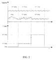
- a comparison between the programming voltage ripples of the prior art solution and of the solution according to the invention shows that the ripple is kept low and constant independently from the number of bits to be programmed as shown in figure 5.
Landscapes
- Engineering & Computer Science (AREA)
- Computer Hardware Design (AREA)
- Read Only Memory (AREA)
Abstract
Description
- The present invention relates to a voltage regulation system for multiword programming in non volatile memories, for example of the Flash type, with low circuit area occupation.
- More particularly, but not exclusively, the invention relates to a system as above and wherein memories comprise at least a memory cell matrix organised in cell rows and columns and with corresponding circuits responsible for addressing, decoding, reading, writing and erasing the memory cell content, said cells having drain terminals connected to the matrix columns and biased in the programming step with a predetermined voltage value by means of program load circuits associated to each matrix column.
- It is known that in modem non volatile memories, for example of the Flash EEPROM type, the need to apply very "precise" voltages to memory cells in the writing step is increasingly felt.
- This is generally valid both for writing cells having a grounded bulk terminal, essentially with Vbulk=0, and for negative Vbulk writing.
- In practise, the requirements of the voltage difference Vdrain - Vbulk can be compared to the requirements of the voltage difference Vdrain-Vsource.
- The term "precise" actually means the observance of two subsequently ordered requirements:
- First of all it must be ensured that the flash cell, during the writing operation, operates within an optimum operation window, i.e. within a well defined region of the plane Vdrain vs L, where L is the cell channel length.
- Such conditions ensure for example a threshold jump required to pass from an erased cell to a programmed cell in the required programming time.
- The parameter L is clearly statistically variable within an array or a matrix; the more this parameter is centred around a nominal value, the more the process, through which the cell matrix is formed, is reliable.
- The second parameter Vdrain will now be analysed. The need to fall anyway within the optimum operation window involves a reduced tolerance on Vdrain (Vdrain = Vnom ± d%) affecting directly the tolerance allowed for the voltage regulator which must generate the drain voltage.
- Actually, in present flash memories only one cell is never written, but a number of cells comprised between 1 and 64.
- When the number of cells to be programmed changes, and thus the total load current Iprogram, the drain voltage regulator must supply a regulated voltage allowing each cell to operate within the operation window.
- Therefore the aim is to succeed in obtaining Vdrain values being as stable as possible or little changed when the number of cells to be programmed changes. Ideally, it should be:
- Vgate=constant or identical ramp for each cell and for each programming operation. There are no great problems in complying with this requirement since the regulator operates on the Flash cell gate terminals and thus on a high impedance load;
- Vbusl=constant identical for each cell and for each programming operation. Also for this requirement there are no great problems in complying with it since the regulator operates on the Flash cell bulk and thus on a high impedance load (if the programming bulk current is disregarded being generally far lower than the drain current);
- Vsource=0 for each cell and for each programming operation. At first sight this is not a very relevant requirement, but it requires a good layout routing and a good bias the source lines.
- The precision requirement for the voltages involved while programming is even stronger in improved flash devices, as in the case of multilevel flash memories wherein the information to be stored in a cell is no more the one of a single bit (for which it is sufficient to verify if the charge is present/ absent on the floating gate) but of a plurality of bits (for which it is necessary to determine indirectly how much charge is present on the floating gate).
- Inaccuracies on programming voltages contribute to increase the distribution widths of the bits represented by each cell which thus make it difficult or even impossible to determine these levels.
- As shown in figures 1 and 2 it is important that the threshold distributions (Vt) of the cells corresponding to the different levels are well spaced from each other in order to make a subsequent sensing easy by using as discriminating voltage (Vr) the voltage in correspondence with the broken lines.
- Inaccuracies at the programming level would lead the various distributions to get closer to each other and even to cross, thus making a subsequent discriminating operation impossible.
- The level distribution in a precise way is a delicate operation which requires a considerable effort as for the memory circuit design.
- From the physical point of view it is clear that a far lower tolerance on cell parameters is required.
- Before facing the regulation problem, it must be immediately said that a design is generally effective if it complies with at least three requirements:
- Quality;
- Area occupation;
- Production or synthesis time
-
- Actually these parameters are different in importance, the failure of one of them can endanger the whole work. An excellent circuit, synthesised in too long times can become obsolete before it is produced and so on.
- One-to-all regulation: it is a kind of regulation shown in figure 3A.
- In this case the regulator directly supplies all the cells requiring it (from 1 to Nmax, with Nmax=8 - 64 or more).
- The regulator must thus regulate the output of a charge pump, in fact in Flash memories writing voltages are usually obtained internally by means of charge pump positive boosters and with a load varying from:
- Bit no. Current
- Iprogram
- Nmax Nmax * Iprogram
-
- With a current in the range of 100uA a load change from 100uA to 6.4mA can occur, Vdrain=Vnom±d% having always to be kept.
- One-to-one regulation: it is a kind of regulation shown in figure 3B.
- In this case there is a regulator for each cell to be programmed.
- The regulator must thus regulate the charge pump output with a load being this time constant.
Bit no. Current
Iprogram - In this case the voltage regulation at the value Vdrain=Vnom±d% is far simpler and more precise.
- Although advantageous under many aspects, this second method has a serious drawback due to the circuit area occupation required by the regulator, being one of the factors to which most attention must be instead drawn in modem memories having an increasingly high integration scale.
- The technical problem underlying the present invention is to provide a voltage regulation system for multiword programming in Flash memories, having such structural and functional characteristics as to require a low circuit area occupation.
- The solution idea underlying the present invention is to form dummy current paths being parallel-associated with program load circuits and enabled by means of pass transistors, for example with enable signals being complementary to the program enabling signal.
- Load current rushes still affecting prior art solutions can therefore be avoided.
- On the basis of this solution idea the technical problem is solved by a system as previously indicated and defined in
claim 1 and the followings. - The features and advantages of the system according to the invention will be apparent from the description of an embodiment thereof given by way of non-limiting example with reference to the attached drawings.
-
- Figure 1 schematically shows a diagram illustrating the threshold voltage distribution in a conventional one-bit-per-cell memory cell;
- Figure 2 schematically shows a diagram illustrating the threshold voltage distribution in a two-bit-per-cell multilevel memory cell;
- Figures 3A and 3B schematically show a portion of a memory cell matrix in a non volatile memory electronic device with an associated column decoder according to the prior art, in the one-to-all and one-to-one regulation cases respectively;
- Figure 4 schematically shows a portion of a memory cell matrix in a non volatile memory electronic device with an associated voltage regulation system according to the invention for the programming step;
- Figure 5 shows by way of comparison some trends of signals inside regulation systems according to the prior art and to the invention.
-
- With reference to the figures, a voltage regulation system for multiword programming in low circuit area occupation non volatile memories, for example of the Flash type, is globally and schematically indicated with 1.
- Non volatile memories are electronic devices integrated on semiconductor and equipped with memory cell matrices, particularly multilevel cells.
- More particularly, memory device means any monolithic electronic system incorporating a matrix of
memory cells 5, organised in rows, referred to asword lines 6, and columns, referred to asbit lines 4, as well as circuit portions associated to the cell matrix and responsible for addressing, decoding, reading, writing and erasing the memory cell content. - Such a device can be for example a memory chip integrated on semiconductor and of the non volatile EEPROM Flash type split in sectors and electrically erasable.
- Each memory cell comprises a floating gate transistor with source S, drain D and control gate G terminals.
- Among the circuit portions associated to the cell matrix
program load circuits 2 are provided, each circuit being associated to acorresponding matrix column 4 and supplied with a specific supply voltage, generated in the integrated memory device and regulated by means of a drain voltage Vd regulator, in order to apply convenient bias voltages to the cell matrix columns. - Moreover, a
column decoder 3 is provided to which the cell matrix columns orbit lines 4 belong. - Also the
column decoder 3, located downstream ofprogram load circuits 2, is supplied with specific voltages generated in the integrated memory circuit by means of positive boosters or charge pumps 12 and regulated by means of corresponding voltage regulators. In the example of figure 3 thecharge pump 12 is regulated by the output of astable voltage regulator 7 through the series of a voltage-controlled oscillator VCO and aphase generator 8. - The principles of the present invention are specifically exploited to perform a local sector regulation of the drain voltage Vd in the programming step.
- The voltage applied to the drain terminal D of
cells 5 is in fact a parameter which must be controlled with great precision during programming. - The principles of the present invention are applied to an integrated memory device wherein the circuit techniques and technological processes used allow an almost constant drain current to be obtained during the whole programming operation.
- Advantageously according to the invention, in parallel with each
program load circuit 2, a conduction-to-ground path 9 enabled by a controlled active element is provided. - The
path 9 comprises apass transistor 10 receiving on the control terminal thereof an enabling signal /PGM. - Moreover, advantageously, said enabling signal is complementary to the enabling signal PGM applied to the corresponding
program load circuit 2. - The
path 9 is essentially a redundant or dummy path. - Therefore, the invention provides dummy
current paths 9 being parallel-associated withprogram load circuits 2 and enabled by means ofpass transistors 10, for example with enabling signals being complementary to the program enablinge signal. - The current value for the
parallel path 9 can thus be easily set, even if its exact value is not important for our application. - In this case this is the regulation of simplest construction since the regulator always operates in a known situation, i.e. as if it were always programming the highest number of cells allowed by the device.
- The invention shares the advantages of known solutions but without being affected by the drawbacks thereof.
- Particularly, the system according to the invention has advantageously a minimum circuit area occupation as in the one-to-all solutions, in fact it requires only the insertion of two transistors for each memory cell branch.
- The system according to the invention has however also the advantage of the one-to-one solution, i.e. it allows a regulation to be performed with almost constant load.
- Essentially, this system avoids load current rushes affecting prior art solutions.
- A comparison between the programming voltage ripples of the prior art solution and of the solution according to the invention shows that the ripple is kept low and constant independently from the number of bits to be programmed as shown in figure 5.
Claims (4)
- A voltage regulation system for multiword programming in non volatile memories, for example of the Flash type, with low circuit area occupation, wherein memories comprise at least a memory cell matrix (5) organised in cell rows and columns and with corresponding circuits responsible for addressing, decoding, reading, writing and erasing the memory cell content, said cells having drain terminals (D) connected to matrix columns and biased in the programming step with a predetermined voltage value by means of program load circuits (2) associated to each matrix column, characterised in that it provides, in parallel with each program load circuit (2), a conduction-to-ground path (9) enabled by a controlled active element (10).
- A system according to claim 1, characterised in that said controlled active element is a pass transistor (10) receiving on the control terminal thereof an enabling signal (/PGM).
- A system according to claim 1, characterised in that said enabling signal is complementary to the enabling signal (PGM) applied to the corresponding program load circuit (2).
- A system according to claim 1, characterised in that said path (9) is essentially a redundant or dummy current path.
Priority Applications (3)
| Application Number | Priority Date | Filing Date | Title |
|---|---|---|---|
| DE60325453T DE60325453D1 (en) | 2003-02-28 | 2003-02-28 | Voltage control system for multibit Programming a compact non-volatile memory with reduced integration area |
| EP03425133A EP1453057B1 (en) | 2003-02-28 | 2003-02-28 | Voltage regulation system for a multibit programming of a reduced integration area non volatile memory |
| US10/789,351 US7139197B2 (en) | 2003-02-28 | 2004-02-26 | Voltage regulation system for a multiword programming of a low integration area non volatile memory |
Applications Claiming Priority (1)
| Application Number | Priority Date | Filing Date | Title |
|---|---|---|---|
| EP03425133A EP1453057B1 (en) | 2003-02-28 | 2003-02-28 | Voltage regulation system for a multibit programming of a reduced integration area non volatile memory |
Publications (2)
| Publication Number | Publication Date |
|---|---|
| EP1453057A1 true EP1453057A1 (en) | 2004-09-01 |
| EP1453057B1 EP1453057B1 (en) | 2008-12-24 |
Family
ID=32749059
Family Applications (1)
| Application Number | Title | Priority Date | Filing Date |
|---|---|---|---|
| EP03425133A Expired - Lifetime EP1453057B1 (en) | 2003-02-28 | 2003-02-28 | Voltage regulation system for a multibit programming of a reduced integration area non volatile memory |
Country Status (3)
| Country | Link |
|---|---|
| US (1) | US7139197B2 (en) |
| EP (1) | EP1453057B1 (en) |
| DE (1) | DE60325453D1 (en) |
Cited By (2)
| Publication number | Priority date | Publication date | Assignee | Title |
|---|---|---|---|---|
| EP1815480A4 (en) * | 2004-11-26 | 2009-03-04 | Atmel Corp | Method and system for regulating a program voltage value during multilevel memory device programming |
| CN112151093A (en) * | 2019-06-26 | 2020-12-29 | 意法半导体股份有限公司 | Non-volatile memory having read circuit operating at low voltage |
Families Citing this family (1)
| Publication number | Priority date | Publication date | Assignee | Title |
|---|---|---|---|---|
| US7936617B2 (en) * | 2007-12-26 | 2011-05-03 | Samsung Electronics Co., Ltd. | Nonvolatile semiconductor memory device |
Citations (2)
| Publication number | Priority date | Publication date | Assignee | Title |
|---|---|---|---|---|
| US6292398B1 (en) * | 1999-05-11 | 2001-09-18 | Stmicroelectronics S.R.L. | Method for the in-writing verification of the threshold value in non-volatile memories |
| US6434051B1 (en) * | 1999-06-24 | 2002-08-13 | Fujitsu Limited | Non-volatile memory circuit |
Family Cites Families (4)
| Publication number | Priority date | Publication date | Assignee | Title |
|---|---|---|---|---|
| US5852578A (en) * | 1997-06-17 | 1998-12-22 | Hoang; Loc B. | Flash cell having self-timed programming |
| IT1319075B1 (en) * | 2000-10-31 | 2003-09-23 | St Microelectronics Srl | IMPULSE PROGRAMMING METHOD IN PARTICULAR FOR HIGH PARALLELISM DIMEMORY DEVICES AND RELATED MEMORY DEVICE |
| ITMI20022570A1 (en) * | 2002-12-05 | 2004-06-06 | Simicroelectronics S R L | PROGRAMMING METHOD OF AN ELECTRICALLY PROGRAMMABLE NON-VOLATILE SEMICONDUCTOR MEMORY |
| ITMI20022569A1 (en) * | 2002-12-05 | 2004-06-06 | Simicroelectronics S R L | PROGRAMMING METHOD OF AN ELECTRONICALLY PROGRAMMABLE NON-VOLATILE SEMICONDUCTOR MEMORY |
-
2003
- 2003-02-28 DE DE60325453T patent/DE60325453D1/en not_active Expired - Lifetime
- 2003-02-28 EP EP03425133A patent/EP1453057B1/en not_active Expired - Lifetime
-
2004
- 2004-02-26 US US10/789,351 patent/US7139197B2/en not_active Expired - Lifetime
Patent Citations (2)
| Publication number | Priority date | Publication date | Assignee | Title |
|---|---|---|---|---|
| US6292398B1 (en) * | 1999-05-11 | 2001-09-18 | Stmicroelectronics S.R.L. | Method for the in-writing verification of the threshold value in non-volatile memories |
| US6434051B1 (en) * | 1999-06-24 | 2002-08-13 | Fujitsu Limited | Non-volatile memory circuit |
Cited By (2)
| Publication number | Priority date | Publication date | Assignee | Title |
|---|---|---|---|---|
| EP1815480A4 (en) * | 2004-11-26 | 2009-03-04 | Atmel Corp | Method and system for regulating a program voltage value during multilevel memory device programming |
| CN112151093A (en) * | 2019-06-26 | 2020-12-29 | 意法半导体股份有限公司 | Non-volatile memory having read circuit operating at low voltage |
Also Published As
| Publication number | Publication date |
|---|---|
| US7139197B2 (en) | 2006-11-21 |
| EP1453057B1 (en) | 2008-12-24 |
| DE60325453D1 (en) | 2009-02-05 |
| US20040233723A1 (en) | 2004-11-25 |
Similar Documents
| Publication | Publication Date | Title |
|---|---|---|
| EP1620860B1 (en) | Memory with uniform read and verification threshold | |
| US7679964B2 (en) | Semiconductor memory device controlling program voltage according to the number of cells to be programmed and method of programming the same | |
| US8233328B2 (en) | Nonvolatile semiconductor memory | |
| KR100769866B1 (en) | Semiconductor memory which has reduced fluctuation of writing speed | |
| US7715230B2 (en) | Method of operating a flash memory device | |
| US6768682B2 (en) | Nonvolatile semiconductor memory and method for controlling programming voltage of nonvolatile semiconductor memory | |
| EP1258007B1 (en) | Wordline driver for flash memory read mode | |
| US20050157556A1 (en) | Nonvolatile memory | |
| EP1123547B1 (en) | Bit line biasing method to eliminate program disturbance in a non-volatile memory device and memory device employing the same | |
| US7184311B2 (en) | Method and system for regulating a program voltage value during multilevel memory device programming | |
| US10930322B2 (en) | Regulator and memory device having the same | |
| KR100648295B1 (en) | Flash memory device and voltage generator circuit for it | |
| US6868012B2 (en) | System and methods for manufacturing non-volatile semiconductor memory apparatus | |
| US5559736A (en) | Non-volatile semiconductor memory device capable of preventing excessive-writing | |
| US7428169B2 (en) | Nonvolatile semiconductor memory device and voltage generating circuit for the same | |
| KR20030014360A (en) | Trimming method and system for wordline booster to minimize process variation of boosted wordline voltage | |
| US7885118B2 (en) | Flash memory device and voltage generating circuit for the same | |
| EP1453057B1 (en) | Voltage regulation system for a multibit programming of a reduced integration area non volatile memory | |
| US7633815B2 (en) | Flexible word line boosting across VCC supply | |
| US7085163B2 (en) | Gate voltage regulation system for a non-volatile memory cells programming and/or soft programming phase | |
| KR100708915B1 (en) | How to reduce capacitive loading in flash memory X-decoders for accurate voltage control on word and select lines | |
| US20070291549A1 (en) | Nonvolatile semiconductor storage apparatus and readout method | |
| CN113450840B (en) | Signal generator and memory device having the same | |
| US7379338B2 (en) | Method and system for regulating a program voltage value during multilevel memory device programming | |
| WO1998008226A1 (en) | A flash memory device having a page mode of operation |
Legal Events
| Date | Code | Title | Description |
|---|---|---|---|
| PUAI | Public reference made under article 153(3) epc to a published international application that has entered the european phase |
Free format text: ORIGINAL CODE: 0009012 |
|
| AK | Designated contracting states |
Kind code of ref document: A1 Designated state(s): AT BE BG CH CY CZ DE DK EE ES FI FR GB GR HU IE IT LI LU MC NL PT SE SI SK TR |
|
| AX | Request for extension of the european patent |
Extension state: AL LT LV MK RO |
|
| 17P | Request for examination filed |
Effective date: 20050228 |
|
| 17Q | First examination report despatched |
Effective date: 20050404 |
|
| AKX | Designation fees paid |
Designated state(s): DE FR GB IT |
|
| RIN1 | Information on inventor provided before grant (corrected) |
Inventor name: SCARDACI, MASSIMO Inventor name: MARTINES, IGNAZIO |
|
| RBV | Designated contracting states (corrected) |
Designated state(s): DE FR GB IT |
|
| GRAC | Information related to communication of intention to grant a patent modified |
Free format text: ORIGINAL CODE: EPIDOSCIGR1 |
|
| GRAP | Despatch of communication of intention to grant a patent |
Free format text: ORIGINAL CODE: EPIDOSNIGR1 |
|
| GRAS | Grant fee paid |
Free format text: ORIGINAL CODE: EPIDOSNIGR3 |
|
| GRAA | (expected) grant |
Free format text: ORIGINAL CODE: 0009210 |
|
| AK | Designated contracting states |
Kind code of ref document: B1 Designated state(s): DE FR GB IT |
|
| REG | Reference to a national code |
Ref country code: GB Ref legal event code: FG4D |
|
| REF | Corresponds to: |
Ref document number: 60325453 Country of ref document: DE Date of ref document: 20090205 Kind code of ref document: P |
|
| PLBE | No opposition filed within time limit |
Free format text: ORIGINAL CODE: 0009261 |
|
| STAA | Information on the status of an ep patent application or granted ep patent |
Free format text: STATUS: NO OPPOSITION FILED WITHIN TIME LIMIT |
|
| GBPC | Gb: european patent ceased through non-payment of renewal fee |
Effective date: 20090324 |
|
| REG | Reference to a national code |
Ref country code: FR Ref legal event code: ST Effective date: 20091030 |
|
| 26N | No opposition filed |
Effective date: 20090925 |
|
| PG25 | Lapsed in a contracting state [announced via postgrant information from national office to epo] |
Ref country code: FR Free format text: LAPSE BECAUSE OF NON-PAYMENT OF DUE FEES Effective date: 20090302 Ref country code: GB Free format text: LAPSE BECAUSE OF NON-PAYMENT OF DUE FEES Effective date: 20090324 |
|
| PG25 | Lapsed in a contracting state [announced via postgrant information from national office to epo] |
Ref country code: IT Free format text: LAPSE BECAUSE OF FAILURE TO SUBMIT A TRANSLATION OF THE DESCRIPTION OR TO PAY THE FEE WITHIN THE PRESCRIBED TIME-LIMIT Effective date: 20081224 |
|
| REG | Reference to a national code |
Ref country code: DE Ref legal event code: R082 Ref document number: 60325453 Country of ref document: DE Representative=s name: SAMSON & PARTNER, PATENTANWAELTE, DE |
|
| REG | Reference to a national code |
Ref country code: DE Ref legal event code: R082 Ref document number: 60325453 Country of ref document: DE Representative=s name: SAMSON & PARTNER, PATENTANWAELTE, DE Effective date: 20130515 Ref country code: DE Ref legal event code: R081 Ref document number: 60325453 Country of ref document: DE Owner name: MICRON TECHNOLOGY, INC., US Free format text: FORMER OWNER: STMICROELECTRONICS S.R.L., AGRATE BRIANZA, IT Effective date: 20130515 Ref country code: DE Ref legal event code: R081 Ref document number: 60325453 Country of ref document: DE Owner name: MICRON TECHNOLOGY, INC., BOISE, US Free format text: FORMER OWNER: STMICROELECTRONICS S.R.L., AGRATE BRIANZA, MAILAND/MILANO, IT Effective date: 20130515 Ref country code: DE Ref legal event code: R082 Ref document number: 60325453 Country of ref document: DE Representative=s name: SAMSON & PARTNER PATENTANWAELTE MBB, DE Effective date: 20130515 Ref country code: DE Ref legal event code: R081 Ref document number: 60325453 Country of ref document: DE Owner name: MICRON TECHNOLOGY, INC., BOISE, US Free format text: FORMER OWNER: STMICROELECTRONICS S.R.L., AGRATE BRIANZA, IT Effective date: 20130515 |
|
| PGFP | Annual fee paid to national office [announced via postgrant information from national office to epo] |
Ref country code: DE Payment date: 20220428 Year of fee payment: 20 |
|
| REG | Reference to a national code |
Ref country code: DE Ref legal event code: R071 Ref document number: 60325453 Country of ref document: DE |