EP1450585A1 - SOLID−STATE SELF−EMISSION DISPLAY AND ITS PRODUCTION METHOD - Google Patents
SOLID−STATE SELF−EMISSION DISPLAY AND ITS PRODUCTION METHOD Download PDFInfo
- Publication number
- EP1450585A1 EP1450585A1 EP02768140A EP02768140A EP1450585A1 EP 1450585 A1 EP1450585 A1 EP 1450585A1 EP 02768140 A EP02768140 A EP 02768140A EP 02768140 A EP02768140 A EP 02768140A EP 1450585 A1 EP1450585 A1 EP 1450585A1
- Authority
- EP
- European Patent Office
- Prior art keywords
- fine particles
- size
- single crystal
- solid state
- fine particle
- Prior art date
- Legal status (The legal status is an assumption and is not a legal conclusion. Google has not performed a legal analysis and makes no representation as to the accuracy of the status listed.)
- Withdrawn
Links
Images


Classifications
-
- H—ELECTRICITY
- H05—ELECTRIC TECHNIQUES NOT OTHERWISE PROVIDED FOR
- H05B—ELECTRIC HEATING; ELECTRIC LIGHT SOURCES NOT OTHERWISE PROVIDED FOR; CIRCUIT ARRANGEMENTS FOR ELECTRIC LIGHT SOURCES, IN GENERAL
- H05B33/00—Electroluminescent light sources
- H05B33/12—Light sources with substantially two-dimensional [2D] radiating surfaces
- H05B33/14—Light sources with substantially two-dimensional [2D] radiating surfaces characterised by the chemical or physical composition or the arrangement of the electroluminescent material, or by the simultaneous addition of the electroluminescent material in or onto the light source
- H05B33/145—Arrangements of the electroluminescent material
-
- H—ELECTRICITY
- H05—ELECTRIC TECHNIQUES NOT OTHERWISE PROVIDED FOR
- H05B—ELECTRIC HEATING; ELECTRIC LIGHT SOURCES NOT OTHERWISE PROVIDED FOR; CIRCUIT ARRANGEMENTS FOR ELECTRIC LIGHT SOURCES, IN GENERAL
- H05B33/00—Electroluminescent light sources
- H05B33/10—Apparatus or processes specially adapted to the manufacture of electroluminescent light sources
-
- H—ELECTRICITY
- H05—ELECTRIC TECHNIQUES NOT OTHERWISE PROVIDED FOR
- H05B—ELECTRIC HEATING; ELECTRIC LIGHT SOURCES NOT OTHERWISE PROVIDED FOR; CIRCUIT ARRANGEMENTS FOR ELECTRIC LIGHT SOURCES, IN GENERAL
- H05B33/00—Electroluminescent light sources
- H05B33/12—Light sources with substantially two-dimensional [2D] radiating surfaces
- H05B33/22—Light sources with substantially two-dimensional [2D] radiating surfaces characterised by the chemical or physical composition or the arrangement of auxiliary dielectric or reflective layers
Definitions
- the present invention relates to solid state light-emissive display apparatus utilizing a quantum size effect and method of manufacturing the same.
- the display apparatuses using liquid crystals are nowadays in wide spread use, but these are not the best in such properties as energy-saving or brightness, since a liquid crystal display apparatus uses backlight in principle. For this reason, the research and development are widely proceeding for a solid state light-emissive display apparatus, aiming to realize high brightness, energy-saving, flat type, and high reliability rather more than liquid crystal.
- EL display apparatus is composed of pixels each of which has a semiconductor layer including light emission center atoms and insulator layers sandwiching said semiconductor layer.
- a light emission center atom such elements that emit visible fluorescence, for example, Mn or rare earth elements are used
- semiconductor layer such semiconductors that have larger band gap energy than visible light, for example, ZnS or else are used
- insulator layers such insulators that have a property which prevents dielectric breakdown of said semiconductor layers, for example, thin films of SiO 2 or Si 3 N 4 are used.
- EL display apparatus emits light as following, electrons in a semiconductor are accelerated by high electric field imposed through insulation layers, the accelerated electrons collide to light emission center atoms to be excited, and the excited light emission center atoms emit fluorescence light. Therefore it is the specific feature of EL display apparatus that electric energy directly converts to light energy.
- FED Field Emission Device
- display apparatuses As the display apparatuses to generate fluorescence by colliding and exciting light emission center atoms by accelerated electron (ballistic electron).
- an FED display apparatus has its problems such that, though it can emit light at relatively low electric field, it requires vacuum space and hence it can not be made to a flat and all-solid state type, since it emits out electrons into vacuum by using a field-emission type electron gun and accelerates them in vacuum.
- the object of the present invention is to provide a solid state light-emissive display apparatus which has much superior properties to existing display apparatuses in brightness, efficiency, reliability, and a thin type. And also the other object of the present invention is to provide a method of manufacturing the said apparatus, which manufactures it at low cost.
- a solid state light-emissive display apparatus characterized in that it has light emitting pixels comprising of a luminous thin film composed of crystal fine particles of nm(nanometer) size coated with insulator and fluorescent fine particles of nm size in a form of laminating of two said each particle layers or in a form of mixed layer of said two particles, and a lower electrode and a transparent upper electrode sandwiching said luminous thin film, whereby to obtain luminous display by impressing alternating voltage or direct current voltage between said upper and lower electrodes.
- said crystal fine particle of nm size coated with insulator is characterized in that it consists of a semiconductor or a metal single crystal fine particle of nm size and insulator film of nm thickness coated the surface of said single crystal fine particle.
- said crystal fine particle of nm is preferably a intrinsic or impurity doped Si single crystal fine particle of nm size
- said insulator film is a SiO 2 film of nm thickness coating the surface of said Si single crystal fine particle.
- said fluorescent fine particle of nm size is a semiconductor fine particle having a band gap energy corresponding to an energy ranging from ultraviolet light to visible light.
- Said fluorescent fine particle of nm size may have a donor or/and an acceptor.
- said fluorescent fine particle of nm size may be a semiconductor fine particle involving luminous atoms or luminous atom ions.
- the voltage impressed between the lower and the upper electrodes are distributed to the insulator films coating the crystal fine particles of nm in the luminous thin film, the electrons injected from the lower electrode are accelerated by the electric field distributed to the insulator film, passes through said insulator film by tunneling or resonant tunneling, and passes through the single crystal fine particle of nm size without being scattered by phonons (Refer to JP 2001-332168, for example).
- the electrons repeat the above mentioned process for each adjacent crystal fine particles of nm size coated with insulator as a result to obtain high kinetic energy, and collide the fluorescent fine particles of nm size. If the kinetic energy of the colliding electron is higher than the band gap energy of the fluorescent fine particle, a free electron and a hole are generated in the fluorescent fine particle, and a free exciton is generated from these free electron and hole.
- the fluorescent fine particle is of nm size, said electron and hole are enclosed in space of nm size, the concentration of said free exciton is raised, and hence the luminous intensity by extinction of said free excitons is increased.
- the generated electron and hole form a bound exciton via a donor or/and an acceptor. Since the fluorescent fine particle is of nm size, the electron and the hole are enclosed in space of nm size, hence the concentration of bound exciton is raised, and the luminous intensity by extinction of said bound excitons is increased.
- fluorescent fine particle including luminous atoms or luminous atom ions
- the apparatus of this invention since electrons can be accelerated without energy loss and exciton concentration can be high, the luminous efficiency and brightness are high. Also, since the luminous thin film is thin and can emit light by itself, the apparatus of this invention can be made extremely thin. Also, since the applied voltage is low, reliability is high.
- the solid state light-emissive display apparatus is characterized in that the upper and the lower electrodes are configurated in a form of matrix configuration, and the intersected region of the upper and the lower electrode are used as a light emitting pixel by simple matrix driven with these electrodes.
- an image display apparatus of high efficiency, high brightness, thin type, and high reliability can be provided.
- the solid state light-emissive display apparatus of the present invention is characterized in that wirings for scanning and wirings for signals are provided in a form of matrix electrode configuration, a thin film transistor is provided at each intersections of said scanning and signal wirings, the gate electrode of said thin film transistor is connected to scanning wiring, the drain electrode of said thin film transistor is connected to signal wiring, the source electrode of said thin film transistor is connected to an electrode of a light emitting pixel , a luminous thin film is sandwiched by said electrode and upper electrode of said light emitting pixel, wherein each light emitting pixels can be actively driven by said each thin film transistors selected by said scanning and signal wirings.
- a method of manufacturing the solid state light-emissive apparatus characterized in that it comprises the steps of: forming Si single crystal fine particles of nm size being floating in an atmosphere by pyrolyzing SiH 4 gas, and conveying said floating Si single crystal fine particles into O 2 gas atmosphere, whereby the surface of said Si single crystal fine particles to be coated with SiO 2 film of nm thickness.
- Si single crystal fine particles are formed in a state of floating and SiO 2 film is formed on the surface of said floating Si single crystal fine particles in a state of floating, Si single crystal fine particles do not contact mutually not to be combined with each other, and hence mutually isolated Si single crystal fine particles coated with SiO 2 film can be provided.
- a solid state light-emissive apparatus can be manufactured by dissolving the crystal fine particles of nm size coated with insulator and the fluorescent fine particles of nm size into respective solvents, soaking a substrate and then taking it out in turn with respective solvents, whereby to laminate the layers of the crystal fine particle of nm size coated with insulator and the layers of fluorescent fine particle of nm size.
- a mono-layer which consists of the crystal fine particles coated with insulator being densely aggregated on the substrate is obtained by one time processing of soaking a substrate into the solvent dissolving the crystal fine particles of nm size coated with insulator and taking out there-from, and the desired thickness of the layer is obtained by repeating the above processing.
- a mono-layer which consists of the fluorescent fine particles of nm size being densely aligned on the layer of the crystal fine particles of nm size coated with insulator on the substrate is obtained by one time processing of soaking the substrate into the solvent dissolving fluorescent fine particles of nm size and taking out there-from, and the desired thickness of the layer is obtained by repeating the above processing.
- the luminous thin film can be provided, in which the crystal fine particle layer of the desired film thickness and the fluorescent fine particle layer of the desired film thickness are laminated.
- those fine particles can be densely packed with only a few gaps between those fine particles in the luminous thin film, it can emit light at high efficiency. And, since no expensive apparatus is needed for the manufacturing, it costs at low.
- the luminous thin film of the solid state light-emissive apparatus can be also manufactured by dissolving the crystal fine particles of nm size coated with insulator and the fluorescent fine particles of nm size into common solvent, by soaking a substrate into the solvent and then taking it out from the solvent, whereby to make a mixed layer of the crystal fine particles of nm size coated with insulator and the fluorescent fine particles of nm size.
- a mono layer which consists of the crystal fine particles coated with insulator and the fluorescent fine particles of nm size being densely and mutually aligned on the substrate, is obtained by one time processing of soaking a substrate into the solvent and taking it out there-from, and the desired thickness of the layer is obtained by repeating the above processing.
- crystal fine particles of nm size coated with insulator preferably consists of a single crystal fine particle of a semiconductor or a metal of nm size coated with insulator film of nm thickness.
- the single crystal fine particle of nm size is preferably a intrinsic or impurity-doped Si single crystal fine particle of nm size
- the insulator film is preferably a SiO 2 film of nm thickness.
- Said fluorescent fine particle of nm size may be a semiconductor fine particle having a band gap energy corresponding to an energy ranging from ultraviolet light to visible light.
- a fluorescent fine particle of nm size may have a donor or/and an acceptor.
- a fluorescent fine particle of nm size may be a semiconductor fine particle involving luminous atoms or luminous atom ions.
- Fig. 1 is a diagrammatic cross-sectional view showing the makeup of a luminous part of a solid state light-emissive display apparatus of the present invention.
- Fig. 1(a) is a drawing showing the makeup of double layer lamination of a layer composed of crystal fine particles coated with insulator layer and a layer composed of fluorescent fine particles layer
- Fig. 1(b) is a drawing showing the makeup of alternate lamination of each one layer composed of crystal fine particles coated with insulator layer and of fluorescent fine particles
- Fig. 1(c) is a drawing showing the makeup of lamination of a mixed layer composed of crystal fine particles coated with insulator layer and fluorescent fine particles.
- a luminous part 1 consists of a lower electrode 2, a luminous thin film 3 laminated on the lower electrode 2, and a transparent upper electrode 4 formed on the luminous thin film 3.
- Said luminous thin film 3 is, in case of Fig. 1(a), consisted of laminating a layer 6 composed of crystal fine particles coated with insulator and a layer 8 composed of fluorescent fine particles 7.
- said luminous thin film 3 is consisted of alternately laminating of a layer 6 composed of crystal fine particles coated with insulator and a layer 8 composed of fluorescent fine particles 7. Further in case of Fig.
- said luminous thin film 3 is consisted of laminating a mixed layer of crystal fine particles coated with insulators 5 and fluorescent fine particles 7.
- Said lower electrode 2 is, for example, n-type high conductive Si substrate 2, and said upper electrode 4 is ITO film which is conductive and transparent to visible light.
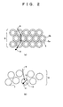
- Fig. 2 is a diagrammatic drawing for explanation of operating principle of a solid state light-emissive display apparatus of the present invention, wherein, Fig. 2(a) shows an enlarged view of layers of crystal fine particles coated with insulator, and Fig. 2(b) shows an enlarged view of layers of fluorescent fine particles.
- said layers 6 are constituted as that crystal fine particles coated with insulator 5 are mutually and densely aligned, and this figure shows for an example where crystal fine particle coated with insulators 5 is Si single crystal fine particle of nm size 5a coated with SiO 2 film of nm thickness 5b.
- crystal fine particle coated with insulators 5 is Si single crystal fine particle of nm size 5a coated with SiO 2 film of nm thickness 5b.
- the diameter of Si single crystal fine particle 5a is 7nm
- the thickness of the SiO 2 film is 3nm.
- said layers 8 are constituted as that fluorescent fine particles 7 are mutually and densely aligned, and said fluorescent fine particle 7 is the semiconductor, for example ZnS, having the band gap energy corresponding to the energy ranging from ultraviolet light to visible light.
- Voltage is applied between the lower electrode 2 and the upper electrode 4 so as to be positively high at the upper electrode 4.
- the voltage are distributed to respective insulators 5b of crystal fine particles coated with insulators 5 constituting the layer 6, that is, SiO 2 film 5b of SiO 2 coated Si single crystal fine particles 5.
- the electrons 9 withdrawn from the lower electrode 2 is accelerated by the electric field distributed to SiO 2 films 5b, and pass through SiO 2 films 5b by tunneling or resonant tunneling transporting phenomenon, since the thickness of SiO 2 film 5b is thin. Since the diameter of a Si single crystal fine particle 5a is small, the electrons in Si single crystal fine particles 5a passes without being scattered by phonons because of quantum size effect, that is, without loss of kinetic energy. As shown in Fig.
- electrons 9 repeat acceleration in SiO 2 film 5b and lossless passing through Si single crystal fine particle 5a at every SiO 2 coated Si single crystal fine particles 5, whereby to obtain a kinetic energy sufficient to excite fluorescent fine particles 7 and to emit from layers 6 composed of SiO 2 coated Si single crystal fine particles.
- the electrons 9 which have obtained the kinetic energy sufficient to excite fluorescent fine particles 7, collide with fluorescent fine particles of nm size 7, and by the collision excitation create free electrons 11 and holes 12 in the conduction band and the valence band of fluorescent fine particles 7.
- Said electrons 11 and said holes 12 form free excitons 13 by coulomb potential based on the respective electric charges. Since these electrons 11 and holes 12 are enclosed inside the fluorescent fine particle of nm size 7, that is, in the space of nm size, their coulomb interaction is strong, and the formation probability of free exciton 13 increases, whereby the free exciton concentration increases. Since the free exciton concentration is high, luminescence intensity generated by extinction of free excitons 13 increases.
- luminescence wavelength can be chosen by choosing the kind of semiconductor. For example, blue color luminescence can be obtained by using ZnS semiconductor, and red color luminescence can be obtained by using GaAs semiconductor.
- the generation efficiency of high energy electrons to excite fluorescent fine particles is quite high, and the exciton concentration is also quite high, therefore, high efficiency and high brightness luminescence can be obtained.
- a fluorescent fine particle 7 is doped with a donor or an acceptor
- an exciton formed via a donor or an acceptor namely a bound exciton 13 is formed.
- a donor and an acceptor are doped
- a bound exciton 13 is formed via a donor and an acceptor.
- electrons 11 and holes 12 are enclosed inside fluorescent fine particles 7, that is, in the space of nm size, their coulomb interaction is very strong, and the formation probability of bound excitons 13 increases, whereby the bound exciton concentration increases. Since the bound exciton concentration is high in this way, luminescence intensity generated by extinction of bound excitons 13 increases.
- the luminescence wavelength corresponding to the depth of energy levels of a donor and an acceptor can be obtained.
- ZnS doped with Al as a donor and Cu as an acceptor provides green light luminescence.
- the accelerated electrons 9 excite the luminous atoms or luminous atom ions by collision excitation, whereby to generate fluorescence of specific wavelength when the luminous atoms or the luminous atom ions transit from the excited state to the ground state.
- Mn is included as luminous atoms in ZnS semiconductor, yellowish orange luminescence can be obtained.
- fluorescent fine particle layers 8 having luminous center atoms can be made to emit light of high brightness.
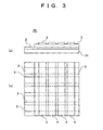
- FIG. 3 shows the makeup of a solid state light-emissive display apparatus of the present invention by simple matrix driving, wherein Fig. 3(a) is a cross-sectional view, and Fig. 3(b) is a plane view.
- a solid state light-emissive display apparatus 30 comprises a substrate 31, the plurality of the lower electrodes 2 in a form of mutually parallel stripes formed on said substrate 31, luminous thin film 3 laminated on said substrate 31 with the lower electrode 2 formed on the same, and the plurality of the upper electrodes 4 in a form of mutually parallel stripes formed on said luminous thin film 3 so to form a perpendicular matrix with said lower electrode 2.
- Said upper electrode 4 is made of transparent ITO film.
- the pixels at arbitrary positions are made luminous.
- FIG. 4 shows the makeup of a solid state light-emissive display apparatus of the present invention by active driving, wherein Fig. 4(a) is a cross-sectional view, and Fig. 4(b) is a plane view.
- a solid state light-emissive display apparatus 40 of the present invention comprises the plurality of the scanning wirings 41 in a form of mutually parallel stripes formed on a substrate 31, the first insulation layer 42 laminated on the substrate 31 having said scanning wirings 41 formed on the substrate, the plurality of the signal wirings 43 in a form of mutually parallel stripes formed on said first insulation layer 42 so to form a perpendicular matrix with said scanning wiring 41, the second insulation layer 44 laminated on said first insulation layer 42 having said signal wirings 43 formed on the first insulation layer 42, the pixel electrodes 45 formed on said second insulation layer 44 and in the proximity of matrix cross sectional region, the luminous thin film 3 laminated on said second insulation layer 44 having pixel electrodes 45 formed on the second insulation layer 44, and the transparent upper electrode 4 covering the whole display surface formed
- a gate electrode 46 of a thin film transistor protruding into the first insulation layer 42 a channel semiconductor layer 47 of a thin film transistor is set opposing to said gate electrode 46 on the first insulation layer 42, one end of said channel 47 is connected to the signal wiring 43 via a drain electrode 48, and the other end of said channel 47 is connected to the pixel electrode 45 via a source electrode 49.
- images and mobile images can be displayed.
- a solid state light-emissive display apparatus of highly efficient and bright luminescence, thin type, and of high reliability can be provided.
- the voltage ratio between a pixel electrode switched on by a thin film transistor and a pixel electrode switched off by a thin film transistor is large, the extinction ratio between pixels becomes high, and so high resolution display is made possible.
- High speed display is also possible because it can be driven with smaller power than by simple matrix system.
- the method of manufacture is first explained in respect to the making of the single crystal fine particles coated with insulator consisting of Si single crystal fine particles coated with SiO 2 film.
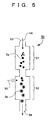
- Fig. 5 is a drawing for explanation of the method of manufacturing of SiO 2 -coated Si single crystal fine particles in accordance with the present invention.
- the manufacturing apparatus 50 has open tube which consists of a part 51 for producing Si single crystal fine particles and a part 52 for coating single crystal fine particles with SiO 2 film, wherein SiH 4 (silane) gas 54 is made to flow into the tube from the inlet 53, SiH 4 gas 54 is pyrolized to form said Si single crystal fine particles 5a of nm size at the part 51 which is held at the pyrolysis temperature of SiH 4 54, and Si single crystal fine particles produced are floating in the atmosphere.
- SiH 4 (silane) gas 54 is made to flow into the tube from the inlet 53
- SiH 4 gas 54 is pyrolized to form said Si single crystal fine particles 5a of nm size at the part 51 which is held at the pyrolysis temperature of SiH 4 54, and Si single crystal fine particles produced are floating in the atmosphere.
- Si single crystal fine particles 5a thus produced are transferred into said part 52 by the gas flow, that is, by flowing gas, or by gravity, and SiO 2 film 5b of nm thickness is formed on the surface of Si single crystal fine particles 5a in the state of floating in the atmosphere by oxygen 55 introduced into a part 52.
- the SiO 2 -coated Si single crystal fine particles 5 thus formed are transferred to the outlet 56 by flowing gas or by gravity and collected.
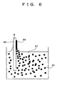
- Fig. 6 is a drawing for explanation of the method of laminating of single crystal fine particles coated with insulator and fluorescent fine particles in accordance with the present invention.
- the figure shows soaking the substrate 62 into the solvent 61 such as water and pulling up said substrate, wherein said substrate62 has the lower electrodes 2 or the pixel electrodes 45 formed on it and in said solvent 61 single crystal fine particles coated with insulator 5 or fluorescent fine particles 7 are dissolved.
- the fine particles 63 which are single crystal fine particles coated with insulator 5 or fluorescent fine particles 7 in the solvent 61 are adhered to the substrate surface 62 so as to minimize the surface free energies such as the surface tension energy of the solvent 61, and the adsorption energy of fine particles 63 to the substrate 62, as the result, a mono layer 64 consisting of the fine particles 63 aligned mutually and densely on the substrate 62 is formed.
- the fine particle layers 64 can be mutually and densely laminated to desired thickness corresponding to the repeating number.
- single crystal fine particles coated with insulator 5 and fluorescent fine particles 7 are dissolved individually in different solvents, and the above mentioned repeating process is repeated with one solvent to laminate to the desired thickness, followed by the repeating process with the other solvent to laminate to the desired thickness.
- single crystal fine particles coated with insulator 5 and fluorescent fine particles 7 are dissolved individually in different solvents, and the above mentioned repeating process is alternately repeated with each solvent to laminate the layer 6 of single crystal fine particles coated with insulator and the layer 8 of fluorescent fine particles alternately one by one.
- the present invention provides a solid state light-emissive display apparatus of dramatically higher brightness and efficiency, higher reliability, and of thinner type than existing display apparatuses. Also in accordance with the present invention, this solid state light-emissive display apparatus can be manufactured at low cost. Thus, if the apparatus of the present invention is used as the display apparatus of mobile phones or others, it is quite useful because of much lower power consumption, higher brightness, thinner type, and higher reliability than existing liquid crystal displays.
Landscapes
- Engineering & Computer Science (AREA)
- Manufacturing & Machinery (AREA)
- Electroluminescent Light Sources (AREA)
- Devices For Indicating Variable Information By Combining Individual Elements (AREA)
- Cathode-Ray Tubes And Fluorescent Screens For Display (AREA)
Abstract
The present invention provides a solid state light-emissive display
apparatus of high brightness and efficiency, high reliability, and of thin type,
and method of manufacturing the same at low cost.
Said apparatus has the luminous thin film made up by laminating or
mixing crystal fine particle coated with insulator (5) of nm size and
fluorescent fine particles (7) of nm size, and the lower electrode and the
transparent upper electrode sandwiching said luminous thin film, wherein
the electrons injected from said lower electrode are accelerated in the crystal
fine particle coated with insulator layer (6) not being scattered by phonons to
become high energy ballistic electrons, and form excitons (13) by colliding
excitation of fluorescent fine particles. Since said fluorescent fine particles are
of nm size, the exciton concentration is high, and luminescence intensity by
extinction of excitons is also high.
Description
The present invention relates to solid state light-emissive display
apparatus utilizing a quantum size effect and method of manufacturing the
same.
The display apparatuses using liquid crystals are lately in wide
spread use, but these are not the best in such properties as energy-saving or
brightness, since a liquid crystal display apparatus uses backlight in principle.
For this reason, the research and development are widely proceeding for a
solid state light-emissive display apparatus, aiming to realize high brightness,
energy-saving, flat type, and high reliability rather more than liquid crystal.
As an existing solid state light-emissive display apparatus, there is
EL(Electro Luminescence) display apparatus. EL display apparatus is
composed of pixels each of which has a semiconductor layer including light
emission center atoms and insulator layers sandwiching said semiconductor
layer. As a light emission center atom, such elements that emit visible
fluorescence, for example, Mn or rare earth elements are used, and as a
semiconductor layer, such semiconductors that have larger band gap energy
than visible light, for example, ZnS or else are used, and as insulator layers,
such insulators that have a property which prevents dielectric breakdown of
said semiconductor layers, for example, thin films of SiO2 or Si3N4 are used.
EL display apparatus emits light as following, electrons in a
semiconductor are accelerated by high electric field imposed through
insulation layers, the accelerated electrons collide to light emission center
atoms to be excited, and the excited light emission center atoms emit
fluorescence light. Therefore it is the specific feature of EL display apparatus
that electric energy directly converts to light energy.
However, there are problems such that light emission efficiency is low
and dielectric breakdown tends to occur, because considerably high electric
field (106 V/cm or higher) is necessary to accelerate the electrons to such a
high energy state ( hot electron state) to emit EL light against the energy
dispersion by phonon scattering. There are also such EL display apparatuses
using organic materials as the semiconductor layer, but they also have
problems such that emission efficiency easily becomes lower as organic
materials are unstable and readily deteriorate.
There are also FED (Field Emission Device) display apparatuses as
the display apparatuses to generate fluorescence by colliding and exciting
light emission center atoms by accelerated electron (ballistic electron).
However, an FED display apparatus has its problems such that, though it can
emit light at relatively low electric field, it requires vacuum space and hence it
can not be made to a flat and all-solid state type, since it emits out electrons
into vacuum by using a field-emission type electron gun and accelerates them
in vacuum.
Taking into consideration the afore-mentioned problems, the object of
the present invention is to provide a solid state light-emissive display
apparatus which has much superior properties to existing display
apparatuses in brightness, efficiency, reliability, and a thin type. And also the
other object of the present invention is to provide a method of manufacturing
the said apparatus, which manufactures it at low cost.
In order to achieve the object mentioned above, there is provided a
solid state light-emissive display apparatus according to the present invention,
characterized in that it has light emitting pixels comprising of a luminous
thin film composed of crystal fine particles of nm(nanometer) size coated with
insulator and fluorescent fine particles of nm size in a form of laminating of
two said each particle layers or in a form of mixed layer of said two particles,
and a lower electrode and a transparent upper electrode sandwiching said
luminous thin film, whereby to obtain luminous display by impressing
alternating voltage or direct current voltage between said upper and lower
electrodes.
In the solid state light-emissive display apparatus according to the
present invention, said crystal fine particle of nm size coated with insulator is
characterized in that it consists of a semiconductor or a metal single crystal
fine particle of nm size and insulator film of nm thickness coated the surface
of said single crystal fine particle.
In the solid state light-emissive display apparatus according to the
present invention, said crystal fine particle of nm is preferably a intrinsic or
impurity doped Si single crystal fine particle of nm size, and said insulator
film is a SiO2 film of nm thickness coating the surface of said Si single
crystal fine particle.
Also preferably, said fluorescent fine particle of nm size is a
semiconductor fine particle having a band gap energy corresponding to an
energy ranging from ultraviolet light to visible light. Said fluorescent fine
particle of nm size may have a donor or/and an acceptor. Also said fluorescent
fine particle of nm size may be a semiconductor fine particle involving
luminous atoms or luminous atom ions.
According to the above mentioned makeup, the voltage impressed
between the lower and the upper electrodes are distributed to the insulator
films coating the crystal fine particles of nm in the luminous thin film, the
electrons injected from the lower electrode are accelerated by the electric field
distributed to the insulator film, passes through said insulator film by
tunneling or resonant tunneling, and passes through the single crystal fine
particle of nm size without being scattered by phonons (Refer to JP
2001-332168, for example). The electrons repeat the above mentioned process
for each adjacent crystal fine particles of nm size coated with insulator as a
result to obtain high kinetic energy, and collide the fluorescent fine particles
of nm size. If the kinetic energy of the colliding electron is higher than the
band gap energy of the fluorescent fine particle, a free electron and a hole are
generated in the fluorescent fine particle, and a free exciton is generated from
these
free electron and hole.
Since the fluorescent fine particle is of nm size, said electron and
hole are enclosed in space of nm size, the concentration of said free exciton is
raised, and hence the luminous intensity by extinction of said free excitons is
increased.
Also, in case that the fluorescent fine particle has a donor or/and an
acceptor, the generated electron and hole form a bound exciton via a donor
or/and an acceptor. Since the fluorescent fine particle is of nm size, the
electron and the hole are enclosed in space of nm size, hence the concentration
of bound exciton is raised, and the luminous intensity by extinction of said
bound excitons is increased.
Also, in the case of fluorescent fine particle including luminous atoms
or luminous atom ions, since the electrons having high kinetic energy are
generated in large quantity by crystal fine particles coated with insulator,
luminous atoms or luminous atom ions in fluorescent fine particles are excited
in large quantity, and luminous intensity is increased.
Thus, according to the present invention, since electrons can be
accelerated without energy loss and exciton concentration can be high, the
luminous efficiency and brightness are high. Also, since the luminous thin
film is thin and can emit light by itself, the apparatus of this invention can be
made extremely thin. Also, since the applied voltage is low, reliability is high.
And, the solid state light-emissive display apparatus according to the
present invention is characterized in that the upper and the lower electrodes
are configurated in a form of matrix configuration, and the intersected region
of the upper and the lower electrode are used as a light emitting pixel by
simple matrix driven with these electrodes.
According to the makeup mentioned above, an image display
apparatus of high efficiency, high brightness, thin type, and high reliability
can be provided.
Further, the solid state light-emissive display apparatus of the
present invention is characterized in that wirings for scanning and wirings for
signals are provided in a form of matrix electrode configuration, a thin film
transistor is provided at each intersections of said scanning and signal
wirings, the gate electrode of said thin film transistor is connected to scanning
wiring, the drain electrode of said thin film transistor is connected to signal
wiring, the source electrode of said thin film transistor is connected to an
electrode of a light emitting pixel ,a luminous thin film is sandwiched by
said electrode and upper electrode of said light emitting pixel, wherein each
light emitting pixels can be actively driven by said each thin film transistors
selected by said scanning and signal wirings.
According to the makeup mentioned above, since the optical
distinction ratio between adjacent pixels can be made high, an image display
apparatus of high efficiency, high brightness, thin type, and high reliability,
and extremely high resolution can be provided.
Next, in order to achieve the other object mentioned above, there is
provided in accordance with the present invention a method of manufacturing
the solid state light-emissive apparatus characterized in that it comprises the
steps of: forming Si single crystal fine particles of nm size being floating in an
atmosphere by pyrolyzing SiH4 gas, and conveying said floating Si single
crystal fine particles into O2 gas atmosphere, whereby the surface of said Si
single crystal fine particles to be coated with SiO2 film of nm thickness.
According to the makeup described above, since the Si single crystal
fine particles are formed in a state of floating and SiO2 film is formed on the
surface of said floating Si single crystal fine particles in a state of floating, Si
single crystal fine particles do not contact mutually not to be combined with
each other, and hence mutually isolated Si single crystal fine particles coated
with SiO2 film can be provided.
By using above mentioned particles, a solid state light-emissive
apparatus can be manufactured by dissolving the crystal fine particles of nm
size coated with insulator and the fluorescent fine particles of nm size into
respective solvents, soaking a substrate and then taking it out in turn with
respective solvents, whereby to laminate the layers of the crystal fine particle
of nm size coated with insulator and the layers of fluorescent fine particle of
nm size.
According to the makeup above mentioned, a mono-layer which
consists of the crystal fine particles coated with insulator being densely
aggregated on the substrate, is obtained by one time processing of soaking a
substrate into the solvent dissolving the crystal fine particles of nm size
coated with insulator and taking out there-from, and the desired thickness of
the layer is obtained by repeating the above processing. Then, a mono-layer
which consists of the fluorescent fine particles of nm size being densely
aligned on the layer of the crystal fine particles of nm size coated with
insulator on the substrate, is obtained by one time processing of soaking the
substrate into the solvent dissolving fluorescent fine particles of nm size and
taking out there-from, and the desired thickness of the layer is obtained by
repeating the above processing. As the result,
the luminous thin film can be provided, in which the crystal fine particle layer
of the desired film thickness and the fluorescent fine particle layer of the
desired film thickness are laminated.
According to the above mentioned method, since those fine particles
can be densely packed with only a few gaps between those fine particles in the
luminous thin film, it can emit light at high efficiency. And, since no
expensive apparatus is needed for the manufacturing, it costs at low.
And the luminous thin film of the solid state light-emissive apparatus
according to the present invention can be also manufactured by dissolving the
crystal fine particles of nm size coated with insulator and the fluorescent fine
particles of nm size into common solvent, by soaking a substrate into the
solvent and then taking it out from the solvent, whereby to make a mixed
layer of the crystal fine particles of nm size coated with insulator and the
fluorescent fine particles of nm size.
According to the above mentioned makeup, a mono layer which
consists of the crystal fine particles coated with insulator and the fluorescent
fine particles of nm size being densely and mutually aligned on the substrate,
is obtained by one time processing of soaking a substrate into the solvent and
taking it out there-from, and the desired thickness of the layer is obtained by
repeating the above processing.
According to the above mentioned method, since those fine particles
can be densely packed with only a few gaps between those fine particles in the
luminous thin film, it can emit light at high efficiency. And, since no
expensive apparatus is needed for the manufacturing, it costs at low.
The afore mentioned crystal fine particles of nm size coated with insulator preferably consists of a single crystal fine particle of a semiconductor or a metal of nm size coated with insulator film of nm thickness.
The afore mentioned crystal fine particles of nm size coated with insulator preferably consists of a single crystal fine particle of a semiconductor or a metal of nm size coated with insulator film of nm thickness.
Also, the single crystal fine particle of nm size is preferably a intrinsic
or impurity-doped Si single crystal fine particle of nm size, and the insulator
film is preferably a SiO2 film of nm thickness.
Said fluorescent fine particle of nm size may be a semiconductor fine
particle having a band gap energy corresponding to an energy ranging from
ultraviolet light to visible light. Also, a fluorescent fine particle of nm size may
have a donor or/and an acceptor. Still further, a fluorescent fine particle of nm
size may be a semiconductor fine particle involving luminous atoms or
luminous atom ions.
The present invention will better be understood from the following
detailed description and the drawings attached hereto showing certain
illustrative forms of embodiment of the present invention; in this connection,
it should be noted that such forms of embodiment illustrated in the
accompanying drawings hereof are intended in no way to limit the present
invention but to facilitate an explanation and an understanding thereof, in
which drawings:
Hereinafter, a detailed explanation is given in respect to
embodiment of the present invention, references being made to figures. In the
drawing figures, it should be noted that the same reference characters are
used to designate substantially the same or corresponding components.
Fig. 1 is a diagrammatic cross-sectional view showing the makeup of
a luminous part of a solid state light-emissive display apparatus of the
present invention. Fig. 1(a) is a drawing showing the makeup of double layer
lamination of a layer composed of crystal fine particles coated with insulator
layer and a layer composed of fluorescent fine particles layer, Fig. 1(b) is a
drawing showing the makeup of alternate lamination of each one layer
composed of crystal fine particles coated with insulator layer and of
fluorescent fine particles, and Fig. 1(c) is a drawing showing the makeup of
lamination of a mixed layer composed of crystal fine particles coated with
insulator layer and fluorescent fine particles.
In Fig. 1, a luminous part 1 consists of a lower electrode 2, a luminous
thin film 3 laminated on the lower electrode 2, and a transparent upper
electrode 4 formed on the luminous thin film 3. Said luminous thin film 3 is, in
case of Fig. 1(a), consisted of laminating a layer 6 composed of crystal fine
particles coated with insulator and a layer 8
composed of fluorescent fine particles 7. Also in case of Fig. 1(b), said
luminous thin film 3 is consisted of alternately laminating of a layer 6
composed of crystal fine particles coated with insulator and a layer 8
composed of fluorescent fine particles 7. Further in case of Fig. 1(c), said
luminous thin film 3 is consisted of laminating a mixed layer of crystal fine
particles coated with insulators 5 and fluorescent fine particles 7. Said lower
electrode 2 is, for example, n-type high conductive Si substrate 2, and said
upper electrode 4 is ITO film which is conductive and transparent to visible
light.
Fig. 2 is a diagrammatic drawing for explanation of operating
principle of a solid state light-emissive display apparatus of the present
invention, wherein, Fig. 2(a) shows an enlarged view of layers of crystal fine
particles coated with insulator, and Fig. 2(b) shows an enlarged view of layers
of fluorescent fine particles.
In Fig. 2(a), said layers 6 are constituted as that crystal fine particles
coated with insulator 5 are mutually and densely aligned, and this figure
shows for an example where crystal fine particle coated with insulators 5 is Si
single crystal fine particle of nm size 5a coated with SiO2 film of nm thickness
5b. Typically in size, the diameter of Si single crystal fine particle 5a is 7nm,
and the thickness of the SiO2 film is 3nm.
In Fig. 2(b), said layers 8 are constituted as that fluorescent fine
particles 7 are mutually and densely aligned, and said fluorescent fine
particle 7 is the semiconductor, for example ZnS, having the band gap energy
corresponding to the energy ranging from ultraviolet light to visible light.
An explanation is next made in respect to luminescence mechanism of
said luminous part.
Voltage is applied between the lower electrode 2 and the upper
electrode 4 so as to be positively high at the upper electrode 4. The voltage are
distributed to respective insulators 5b of crystal fine particles coated with
insulators 5 constituting the layer 6, that is, SiO2 film 5b of SiO2 coated Si
single crystal fine particles 5. The electrons 9 withdrawn from the lower
electrode 2 is accelerated by the electric field distributed to SiO2 films 5b, and
pass through SiO2 films 5b by tunneling or resonant tunneling transporting
phenomenon, since the thickness of SiO2 film 5b is thin. Since the diameter of
a Si single crystal fine particle 5a is small, the electrons in Si single crystal
fine particles 5a passes without being scattered by phonons because of
quantum size effect, that is, without loss of kinetic energy. As shown in Fig.
2(a), electrons 9 repeat acceleration in SiO2 film 5b and lossless passing
through Si single crystal fine particle 5a at every SiO2 coated Si single crystal
fine particles 5, whereby to obtain a kinetic energy sufficient to excite
fluorescent fine particles 7 and to emit from layers 6 composed of SiO2 coated
Si single crystal fine particles.
As shown in Fig. 2(b), the electrons 9 which have obtained the kinetic
energy sufficient to excite fluorescent fine particles 7, collide with fluorescent
fine particles of nm size 7, and by the collision excitation create free electrons
11 and holes 12 in the conduction band and the valence band of fluorescent
fine particles 7. Said electrons 11 and said holes 12 form free excitons 13 by
coulomb potential based on the respective electric charges. Since these
electrons 11 and holes 12 are enclosed inside the fluorescent fine particle of
nm size 7, that is, in the space of nm size, their coulomb interaction is strong,
and the formation probability of free exciton 13 increases, whereby the free
exciton concentration increases. Since the free exciton concentration is high,
luminescence intensity generated by extinction of free excitons 13 increases.
Since the free exciton energy depends on the band gap energy of the
semiconductor crystal, luminescence wavelength can be chosen by choosing
the kind of semiconductor. For example, blue color luminescence can be
obtained by using ZnS semiconductor, and red color luminescence can be
obtained by using GaAs semiconductor.
Thus, in accordance with the present invention, the generation
efficiency of high energy electrons to excite fluorescent fine particles is quite
high, and the exciton concentration is also quite high, therefore, high
efficiency and high brightness luminescence can be obtained.
Also, since electrons 9 are not scattered by phonons in the process of
acceleration, dielectric breakdown of crystal fine particle coated with
insulators 5 does not tend to occur. Consequently, since it is possible to make
the thickness of fluorescent thin film 3 extremely thin to raise the electric
field intensity, a solid state light-emissive display apparatus which is
extremely thin type and has high reliability can be obtained.
Also in case that a fluorescent fine particle 7 is doped with a donor or
an acceptor, an exciton formed via a donor or an acceptor, namely a bound
exciton 13 is formed. In case that a donor and an acceptor are doped, a bound
exciton 13 is formed via a donor and an acceptor. In this case, too, since
electrons 11 and holes 12 are enclosed inside fluorescent fine particles 7, that
is, in the space of nm size, their coulomb interaction is very strong, and the
formation probability of bound excitons 13 increases, whereby the bound
exciton concentration increases. Since the bound exciton concentration is high
in this way, luminescence intensity generated by extinction of bound excitons
13 increases. Also in this case, the luminescence wavelength corresponding to
the depth of energy levels of a donor and an acceptor can be obtained. For
example, ZnS doped with Al as a donor and Cu as an acceptor provides green
light luminescence. Also, by using a semiconductor including luminous atoms
or luminous atom ions for fluorescent fine particles 7, the accelerated
electrons 9 excite the luminous atoms or luminous atom ions by collision
excitation, whereby to generate fluorescence of specific wavelength when the
luminous atoms or the luminous atom ions transit from the excited state to
the ground state. For example, if Mn is included as luminous atoms in ZnS
semiconductor, yellowish orange luminescence can be obtained.
According to the present invention, since electrons 9 can be
accelerated at quite high efficiency, fluorescent fine particle layers 8 having
luminous center atoms can be made to emit light of high brightness.
As described above, according to the present invention, electrons can
be accelerated at quite high efficiency. Theoretically mentioned, since
electrons can be accelerated without energy loss, it is possible to obtain
luminescence with an applied voltage corresponding to the band gap energy of
fluorescent fine particles. For example, if ZnS semiconductor is used as
semiconductor of fluorescent fine particles, luminescence is obtained with the
applied voltage of about 4V, because the band gap energy of ZnS is about 3.7
eV. Consequently, luminescence of high brightness is possible also by the
makeup of Fig. 1(b) and (c).
An explanation is next given in respect to a solid state light-emissive
display apparatus of the present invention by simple matrix driving.
Fig. 3 shows the makeup of a solid state light-emissive display
apparatus of the present invention by simple matrix driving, wherein Fig. 3(a)
is a cross-sectional view, and Fig. 3(b) is a plane view. A solid state
light-emissive display apparatus 30 comprises a substrate 31, the plurality of
the lower electrodes 2 in a form of mutually parallel stripes formed on said
substrate 31, luminous thin film 3 laminated on said substrate 31 with the
lower electrode 2 formed on the same, and the plurality of the upper
electrodes 4 in a form of mutually parallel stripes formed on said luminous
thin film 3 so to form a perpendicular matrix with said lower electrode 2. Said
upper electrode 4 is made of transparent ITO film.
By making the cross-sectional regions of the lower electrode 2 and the
upper electrode 4 as pixels, choosing an arbitrary one set from the plurality of
the lower electrodes 2 and the plurality of the upper electrodes 4, and by
applying a voltage between the lower electrodes 2 and the upper electrodes 4,
the pixels at arbitrary positions are made luminous.
In accordance with the above mentioned, images and mobile images
can be displayed. Since the luminous thin film explained in Fig. 1 and Fig. 2 is
used, a solid state light-emissive display apparatus 30 of high efficiency and
high brightness luminescence, thin type, and high reliability is provided.
An explanation is next given in respect to a solid state light-emissive
display apparatus of the present invention by active driving.
Fig. 4 shows the makeup of a solid state light-emissive display
apparatus of the present invention by active driving, wherein Fig. 4(a) is a
cross-sectional view, and Fig. 4(b) is a plane view. A solid state light-emissive
display apparatus 40 of the present invention comprises the plurality of the
scanning wirings 41 in a form of mutually parallel stripes formed on a
substrate 31, the first insulation layer 42 laminated on the substrate 31
having said scanning wirings 41 formed on the substrate, the plurality of the
signal wirings 43 in a form of mutually parallel stripes formed on said first
insulation layer 42 so to form a perpendicular matrix with said scanning
wiring 41, the second insulation layer 44 laminated on said first insulation
layer 42 having said signal wirings 43 formed on the first insulation layer 42,
the pixel electrodes 45 formed on said second insulation layer 44 and in the
proximity of matrix cross sectional region, the luminous thin film 3 laminated
on said second insulation layer 44 having pixel electrodes 45 formed on the
second insulation layer 44, and the transparent upper electrode 4 covering the
whole display surface formed on said luminous thin film 3.
Near matrix cross sectional region and on said scanning wiring 41 is
set a gate electrode 46 of a thin film transistor protruding into the first
insulation layer 42, a channel semiconductor layer 47 of a thin film transistor
is set opposing to said gate electrode 46 on the first insulation layer 42, one
end of said channel 47 is connected to the signal wiring 43 via a drain
electrode 48, and the other end of said channel 47 is connected to the pixel
electrode 45 via a source electrode 49.
In accordance with the above mentioned, images and mobile images
can be displayed. As a luminous thin film explained in Figs. 1 and 2 is used in
the present invention, a solid state light-emissive display apparatus of highly
efficient and bright luminescence, thin type, and of high reliability can be
provided. Also according to the present makeup, since the voltage ratio
between a pixel electrode switched on by a thin film transistor and a pixel
electrode switched off by a thin film transistor is large, the extinction ratio
between pixels becomes high, and so high resolution display is made possible.
High speed display is also possible because it can be driven with smaller
power than by simple matrix system.
Explanation is next given in respect to the method of manufacture of
a solid state light-emissive display apparatus of the present invention.
The method of manufacture is first explained in respect to the making
of the single crystal fine particles coated with insulator consisting of Si single
crystal fine particles coated with SiO2 film.
Fig. 5 is a drawing for explanation of the method of manufacturing of
SiO2-coated Si single crystal fine particles in accordance with the present
invention. In this figure, the manufacturing apparatus 50 has open tube
which consists of a part 51 for producing Si single crystal fine particles and a
part 52 for coating single crystal fine particles with SiO2 film, wherein SiH4
(silane) gas 54 is made to flow into the tube from the inlet 53, SiH4 gas 54 is
pyrolized to form said Si single crystal fine particles 5a of nm size at the part
51 which is held at the pyrolysis temperature of SiH 4 54, and Si single crystal
fine particles produced are floating in the atmosphere. Si single crystal fine
particles 5a thus produced are transferred into said part 52 by the gas flow,
that is, by flowing gas, or by gravity, and SiO2 film 5b of nm thickness is
formed on the surface of Si single crystal fine particles 5a in the state of
floating in the atmosphere by oxygen 55 introduced into a part 52. The
SiO2-coated Si single crystal fine particles 5 thus formed are transferred to
the outlet 56 by flowing gas or by gravity and collected.
By the method mentioned above, it is possible to produce SiO2-coated
Si single crystal fine particles mutually separated without forming porous
aggregate formed by mutual contact of said single crystal fine particles.
Explanation is next made in respect to the formation of luminous thin
film by laminating of single crystal fine particles coated with insulator and
fluorescent fine particles on a substrate.
Fig. 6 is a drawing for explanation of the method of laminating of
single crystal fine particles coated with insulator and fluorescent fine
particles in accordance with the present invention.
The figure shows soaking the substrate 62 into the solvent 61 such as
water and pulling up said substrate, wherein said substrate62 has the lower
electrodes 2 or the pixel electrodes 45 formed on it and in said solvent 61
single crystal fine particles coated with insulator 5 or fluorescent fine
particles 7 are dissolved. The fine particles 63 which are single crystal fine
particles coated with insulator 5 or fluorescent fine particles 7 in the solvent
61 are adhered to the substrate surface 62 so as to minimize the surface free
energies such as the surface tension energy of the solvent 61, and the
adsorption energy of fine particles 63 to the substrate 62, as the result, a
mono layer 64 consisting of the fine particles 63 aligned mutually and densely
on the substrate 62 is formed.
By the repeating of soaking and pulling up of the substrate 62, the
fine particle layers 64 can be mutually and densely laminated to desired
thickness corresponding to the repeating number.
In order to form the luminous thin film 3 of the makeup shown in Fig.
1(a), single crystal fine particles coated with insulator 5 and fluorescent fine
particles 7 are dissolved individually in different solvents, and the above
mentioned repeating process is repeated with one solvent to laminate to the
desired thickness, followed by the repeating process with the other solvent to
laminate to the desired thickness.
In order to form the luminous thin film 3 of the makeup shown in Fig.
1(b), single crystal fine particles coated with insulator 5 and fluorescent fine
particles 7 are dissolved individually in different solvents, and the above
mentioned repeating process is alternately repeated with each solvent to
laminate the layer 6 of single crystal fine particles coated with insulator and
the layer 8 of fluorescent fine particles alternately one by one.
In order to form the luminous thin film 3 of the makeup shown in Fig.
1(c), single crystal fine particles coated with insulator 5 and fluorescent fine
particles 7 are dissolved in a common solvent, the above mentioned repeating
process is repeated with the common solvent to laminate the mixed layer of
crystal fine particles coated with insulator 5 and fluorescent fine particles 7 to
the desired thickness.
Since fine particles are aligned densely with few gaps in the luminous
thin film thus formed, the electric field distribution is uniform, tunneling
probability increases, and electrons can be accelerated at high efficiency. Also,
brightness is high because fluorescent fine particles are densely aligned.
As will have been appreciated from the foregoing description, the
present invention provides a solid state light-emissive display apparatus of
dramatically higher brightness and efficiency, higher reliability, and of
thinner type than existing display apparatuses. Also in accordance with the
present invention, this solid state light-emissive display apparatus can be
manufactured at low cost. Thus, if the apparatus of the present invention is
used as the display apparatus of mobile phones or others, it is quite useful
because of much lower power consumption, higher brightness, thinner type,
and higher reliability than existing liquid crystal displays.
Claims (16)
- A solid state light-emissive display apparatus, characterized in that it comprises:whereby to obtain luminous display by impressing alternating voltage or direct current voltage between said upper and lower electrodes.a luminous part comprising a luminous thin film composed of laminated or mixed of crystal fine particles coated with insulator of nm (nanometer) size and fluorescent fine particles of nm size; anda lower electrode and a transparent upper electrode sandwiching said luminous thin film,
- A solid state light-emissive display apparatus as set forth in Claim 1, characterized in that:said crystal fine particles coated with insulator of nm size consist of single crystal fine particle of nm size of either a semiconductor or a metal, and an insulator film of nm thickness coating the surface of said single crystal fine particle.
- A solid state light-emissive display apparatus as set forth in Claim 2, characterized in that:said single crystal fine particles of nm size are either intrinsic Si single crystal fine particles of nm size or those doped with impurities,and said insulator film is SiO2 film of nm thickness coating the surface of said Si single crystal fine particles.
- A solid state light-emissive display apparatus as set forth in Claim 1, characterized in that:said fluorescent fine particles of nm size are the semiconductor fine particles having a band gap energy corresponding to an energy ranging from ultraviolet light to visible light.
- A solid state light-emissive display apparatus as set forth in Claim 4, characterized in that:said fluorescent fine particles of nm size have either a donor or/and an acceptor.
- A solid state light-emissive display apparatus as set forth in Claims 4 or 5, characterized in that:said fluorescent fine particles of nm size are the semiconductor fine particles involved with either a luminous atoms or a luminous atom ions.
- A solid state light-emissive display apparatus as set forth in Claim 1, characterized in that:said upper and lower electrodes are formed in a form of matrix configuration, and intersection regions of said upper and lower electrodes are used as pixels which are driven by simple matrix driven operation.
- A solid state light-emissive display apparatus as set forth in Claim 1, characterized in that:scanning wirings and signal wirings are formed in a form of matrix, a thin film transistor is set at an intersection region of said scanning wiring and said signal wiring, a gate electrode of said thin film transistor is connected to said scanning wiring, a drain electrode of said thin film transistor is connected to said signal wiring, a source electrode of said thin film transistor is connected to a pixel electrode, said luminous thin film is sandwiched by said pixel electrode and said upper electrode,whereby each said pixels are actively driven by said thin film transistors by choosing said scanning wiring and signal wiring.
- A method of manufacturing of a solid state light-emissive apparatus, characterized in that it comprises steps:producing Si single crystal fine particles of nm size by pyrolyzing SiH4 in a floating state of said Si single crystal fine particles in atmosphere;transferring said Si single crystal fine particles in the state of floating into O2 gas atmosphere; andcoating the surface of said Si single crystal fine particles with SiO2 film of nm thickness.
- A method of manufacturing of a solid state light-emissive apparatus, characterized in that it comprises steps:dissolving crystal fine particles coated with insulator of nm size and fluorescent fine particles of nm size into respective solvents; andsoaking a substrate into each solvents and pulling it up, whereby laminating of a single crystal fine particle layer and a fluorescent fine particle layer.
- A method of manufacturing of a solid state light-emissive apparatus, characterized in that it comprises steps:dissolving crystal fine particle coated with insulator of nm size and fluorescent fine particles of nm size into common solvent; andsoaking a substrate into said solvent and pulling it up, whereby laminating a mixed layer composed of single crystal fine particles coated with insulator and fluorescent fine particles.
- A method of manufacturing of a solid state light-emissive apparatus as set forth in Claim 10 or 11, characterized in that:said crystal fine particle coated with insulator of nm size consists of a single crystal fine particle of nm size of either a semiconductor or a metal, and a insulator film of nm thickness coating the surface of said single crystal fine particle.
- A method of manufacturing of a solid state light-emissive apparatus as set forth in Claim 12, characterized in that:said single crystal fine particle of nm size is either intrinsic Si single crystal fine particle of nm size or that doped with impurity, and said insulator film is SiO2 film of nm thickness coating the surface of said Si single crystal fine particle.
- A method of manufacturing of a solid state light-emissive apparatus as set forth in Claim 10 or 11, characterized in that:said fluorescent fine particle of nm size is a semiconductor fine particle having a band gap energy corresponding to an energy ranging from ultraviolet light to visible light .
- A method of manufacturing of a solid state light-emissive apparatus as set forth in Claim 10 or 11, characterized in that:said fluorescent fine particle of nm size has a donor or/and an acceptor.
- A method of manufacturing of a solid state light-emissive apparatus as set forth in Claim 14 or 15, characterized in that:said fluorescent fine particle of nm size is a semiconductor fine particle involving a luminous atoms or a luminous atom ions.
Applications Claiming Priority (3)
| Application Number | Priority Date | Filing Date | Title |
|---|---|---|---|
| JP2001305857A JP3613792B2 (en) | 2001-10-01 | 2001-10-01 | Solid-state self-luminous display device and manufacturing method thereof |
| JP2001305857 | 2001-10-01 | ||
| PCT/JP2002/010190 WO2003032690A1 (en) | 2001-10-01 | 2002-09-30 | Solid-state self-emission display and its production method |
Publications (2)
| Publication Number | Publication Date |
|---|---|
| EP1450585A1 true EP1450585A1 (en) | 2004-08-25 |
| EP1450585A4 EP1450585A4 (en) | 2009-07-08 |
Family
ID=19125582
Family Applications (1)
| Application Number | Title | Priority Date | Filing Date |
|---|---|---|---|
| EP02768140A Withdrawn EP1450585A4 (en) | 2001-10-01 | 2002-09-30 | SOLID STATE SPONTANEOUS EMISSION SCREEN AND METHOD FOR PRODUCING THE SAME |
Country Status (4)
| Country | Link |
|---|---|
| US (1) | US7053422B2 (en) |
| EP (1) | EP1450585A4 (en) |
| JP (1) | JP3613792B2 (en) |
| WO (1) | WO2003032690A1 (en) |
Families Citing this family (21)
| Publication number | Priority date | Publication date | Assignee | Title |
|---|---|---|---|---|
| US7428510B2 (en) * | 2000-02-25 | 2008-09-23 | Telecommunication Systems, Inc. | Prepaid short messaging |
| CN100484351C (en) * | 2003-06-13 | 2009-04-29 | 松下电器产业株式会社 | Light-emitting device, method for producing same, and display |
| WO2004112440A1 (en) * | 2003-06-13 | 2004-12-23 | Matsushita Electric Industrial Co., Ltd. | Light-emitting device, method for producing same, and display |
| JP4669786B2 (en) * | 2003-07-02 | 2011-04-13 | パナソニック株式会社 | Display device |
| US7982390B2 (en) | 2003-07-02 | 2011-07-19 | Panasonic Corporation | Light emitting element and display device having an inorganic phosphor layer |
| JPWO2005004546A1 (en) * | 2003-07-02 | 2006-08-17 | 松下電器産業株式会社 | Electroluminescent device and display device |
| JPWO2005004545A1 (en) * | 2003-07-02 | 2006-08-17 | 松下電器産業株式会社 | Light emitting element and display device |
| US20060181197A1 (en) * | 2004-07-01 | 2006-08-17 | Kumio Nago | Electroluminescent device and display |
| JP4776955B2 (en) | 2005-03-17 | 2011-09-21 | キヤノン株式会社 | Light emitting device and manufacturing method thereof |
| JP4303308B2 (en) | 2007-11-20 | 2009-07-29 | シャープ株式会社 | Electron-emitting device, electron-emitting device, self-luminous device, image display device, air blower, cooling device, charging device, image forming device, electron beam curing device, and method for manufacturing electron-emitting device |
| JP4314307B1 (en) * | 2008-02-21 | 2009-08-12 | シャープ株式会社 | Heat exchanger |
| US8299700B2 (en) | 2009-02-05 | 2012-10-30 | Sharp Kabushiki Kaisha | Electron emitting element having an electron acceleration layer, electron emitting device, light emitting device, image display device, cooling device, and charging device |
| CN101814405B (en) | 2009-02-24 | 2012-04-25 | 夏普株式会社 | Electron emitting element, method for producing electron emitting element and each device using the same |
| JP5073721B2 (en) * | 2009-05-19 | 2012-11-14 | シャープ株式会社 | Electron-emitting device, electron-emitting device, self-luminous device, image display device, air blower, cooling device, charging device, image forming device, electron beam curing device, and electron-emitting device manufacturing method |
| JP4932873B2 (en) | 2009-05-19 | 2012-05-16 | シャープ株式会社 | Self-light-emitting element, self-light-emitting device, image display device, self-light-emitting element driving method, and method of manufacturing self-light-emitting element |
| JP4777448B2 (en) | 2009-05-19 | 2011-09-21 | シャープ株式会社 | Electron emitting device, electron emitting device, self-luminous device, image display device, blower device, cooling device, charging device, image forming device, and electron beam curing device |
| JP4732534B2 (en) | 2009-05-19 | 2011-07-27 | シャープ株式会社 | Electron emitting element, electron emitting device, charging device, image forming device, electron beam curing device, self-luminous device, image display device, blower, cooling device |
| JP4732533B2 (en) | 2009-05-19 | 2011-07-27 | シャープ株式会社 | Electron-emitting device and manufacturing method thereof, and electron-emitting device, charging device, image forming device, electron beam curing device, self-luminous device, image display device, blower, and cooling device |
| CN101930884B (en) | 2009-06-25 | 2012-04-18 | 夏普株式会社 | Electron emitting element and method for producing electron emitting element, electron emitting device, self luminescence device and image display device |
| JP4927152B2 (en) * | 2009-11-09 | 2012-05-09 | シャープ株式会社 | Heat exchanger |
| JP4880740B2 (en) | 2009-12-01 | 2012-02-22 | シャープ株式会社 | Electron-emitting device and manufacturing method thereof, and electron-emitting device, charging device, image forming device, electron beam curing device, self-luminous device, image display device, blower, and cooling device |
Family Cites Families (15)
| Publication number | Priority date | Publication date | Assignee | Title |
|---|---|---|---|---|
| US5229628A (en) * | 1989-08-02 | 1993-07-20 | Nippon Sheet Glass Co., Ltd. | Electroluminescent device having sub-interlayers for high luminous efficiency with device life |
| JPH0636900B2 (en) * | 1990-09-26 | 1994-05-18 | 工業技術院長 | Method for forming LB film |
| JPH05206515A (en) * | 1991-12-27 | 1993-08-13 | Victor Co Of Japan Ltd | Ultrafine particle light emitting device and manufacturing apparatus thereof |
| EP0622439A1 (en) * | 1993-04-20 | 1994-11-02 | Koninklijke Philips Electronics N.V. | Quantum sized activator doped semiconductor particles |
| DE19502541A1 (en) * | 1995-01-27 | 1996-08-08 | Bosch Gmbh Robert | Electroluminescent system |
| JPH08250764A (en) * | 1995-03-10 | 1996-09-27 | Toshiba Corp | Semiconductor light emitting device |
| DE19518668A1 (en) * | 1995-05-22 | 1996-11-28 | Bosch Gmbh Robert | Electroluminescent layer system |
| JP3540445B2 (en) * | 1995-06-14 | 2004-07-07 | 明 田崎 | MIM / MIS electron source and method of manufacturing the same |
| JPH0992167A (en) | 1995-09-19 | 1997-04-04 | Toshiba Corp | Phosphor screen |
| US6143201A (en) * | 1997-10-28 | 2000-11-07 | Nec Corporation | Method of manufacturing fluorescent material |
| AUPP004497A0 (en) * | 1997-10-28 | 1997-11-20 | University Of Melbourne, The | Stabilized particles |
| JP2000164921A (en) * | 1998-11-26 | 2000-06-16 | Mitsubishi Materials Corp | Semiconductor light emitting material, method of manufacturing the same, and light emitting device using the same |
| JP3988309B2 (en) * | 1999-01-14 | 2007-10-10 | ソニー株式会社 | Phosphor and method for producing the same |
| JP2001155858A (en) * | 1999-11-24 | 2001-06-08 | Sharp Corp | Manufacturing method of organic EL element |
| JP3806751B2 (en) | 2000-05-23 | 2006-08-09 | 独立行政法人科学技術振興機構 | Quantum size effect type micro electron gun manufacturing method |
-
2001
- 2001-10-01 JP JP2001305857A patent/JP3613792B2/en not_active Expired - Fee Related
-
2002
- 2002-09-30 WO PCT/JP2002/010190 patent/WO2003032690A1/en not_active Ceased
- 2002-09-30 US US10/490,660 patent/US7053422B2/en not_active Expired - Fee Related
- 2002-09-30 EP EP02768140A patent/EP1450585A4/en not_active Withdrawn
Also Published As
| Publication number | Publication date |
|---|---|
| JP2003115385A (en) | 2003-04-18 |
| US20040246408A1 (en) | 2004-12-09 |
| EP1450585A4 (en) | 2009-07-08 |
| US7053422B2 (en) | 2006-05-30 |
| JP3613792B2 (en) | 2005-01-26 |
| WO2003032690A1 (en) | 2003-04-17 |
Similar Documents
| Publication | Publication Date | Title |
|---|---|---|
| US7053422B2 (en) | Solid-state self-emission display and its production method | |
| US5882779A (en) | Semiconductor nanocrystal display materials and display apparatus employing same | |
| Kim et al. | Performance of light-emitting-diode based on quantum dots | |
| US9574134B2 (en) | Light emitting device including semiconductor nanocrystals | |
| CN103346265B (en) | A kind of luminescent device, display floater and manufacture method thereof | |
| US10263220B2 (en) | Manufacturing method for QLED display | |
| KR20090050048A (en) | Luminescent Materials with Nano Crystals Representing Multi-Mode Energy Level Distributions | |
| JP2005038634A (en) | Current injection type light emitting device | |
| JP2010055900A (en) | Electroluminescent element | |
| EP0258908B1 (en) | Ultrafine grain fluorescent body | |
| JPH08250281A (en) | Luminescent element and displaying apparatus | |
| JP5191476B2 (en) | Display device | |
| JP5014347B2 (en) | Display device | |
| JP2006127780A (en) | Electroluminescent device | |
| JPH04280094A (en) | Thin film light-emitting device | |
| CN109616504A (en) | Display panel | |
| CN1949434A (en) | Light emitting device using electron emission and flat display apparatus using the same | |
| Munasinghe et al. | High brightness ZnS and GaN electroluminescent devices using PZT thick dielectric layers | |
| JP2006120328A (en) | Dispersion type EL device | |
| CN203288188U (en) | Two-sided displaying device | |
| Kobayashi et al. | Research on inorganic electroluminescence–present status | |
| KR100405134B1 (en) | A manufacturing process electro luminescence device | |
| KR100455288B1 (en) | Flat panel display apparatus using silicon light emitting device | |
| US20240298497A1 (en) | Light emitting device, light emitting substrate and light emitting apparatus | |
| CN1167311C (en) | Mixed excitation and light-emitting flat panel display device |
Legal Events
| Date | Code | Title | Description |
|---|---|---|---|
| PUAI | Public reference made under article 153(3) epc to a published international application that has entered the european phase |
Free format text: ORIGINAL CODE: 0009012 |
|
| 17P | Request for examination filed |
Effective date: 20040427 |
|
| AK | Designated contracting states |
Kind code of ref document: A1 Designated state(s): AT BE BG CH CY CZ DE DK EE ES FI FR GB GR IE IT LI LU MC NL PT SE SK TR |
|
| RAP1 | Party data changed (applicant data changed or rights of an application transferred) |
Owner name: JAPAN SCIENCE AND TECHNOLOGY AGENCY |
|
| A4 | Supplementary search report drawn up and despatched |
Effective date: 20090610 |
|
| 17Q | First examination report despatched |
Effective date: 20090929 |
|
| STAA | Information on the status of an ep patent application or granted ep patent |
Free format text: STATUS: THE APPLICATION IS DEEMED TO BE WITHDRAWN |
|
| 18D | Application deemed to be withdrawn |
Effective date: 20100210 |