EP1450397A2 - Wet Clean method PZT Capacitors - Google Patents
Wet Clean method PZT Capacitors Download PDFInfo
- Publication number
- EP1450397A2 EP1450397A2 EP04100724A EP04100724A EP1450397A2 EP 1450397 A2 EP1450397 A2 EP 1450397A2 EP 04100724 A EP04100724 A EP 04100724A EP 04100724 A EP04100724 A EP 04100724A EP 1450397 A2 EP1450397 A2 EP 1450397A2
- Authority
- EP
- European Patent Office
- Prior art keywords
- layer
- pzt
- capacitor
- phosphoric acid
- conductive layers
- Prior art date
- Legal status (The legal status is an assumption and is not a legal conclusion. Google has not performed a legal analysis and makes no representation as to the accuracy of the status listed.)
- Withdrawn
Links
Images

Classifications
-
- H—ELECTRICITY
- H10—SEMICONDUCTOR DEVICES; ELECTRIC SOLID-STATE DEVICES NOT OTHERWISE PROVIDED FOR
- H10D—INORGANIC ELECTRIC SEMICONDUCTOR DEVICES
- H10D1/00—Resistors, capacitors or inductors
- H10D1/60—Capacitors
- H10D1/68—Capacitors having no potential barriers
- H10D1/682—Capacitors having no potential barriers having dielectrics comprising perovskite structures
-
- H—ELECTRICITY
- H10—SEMICONDUCTOR DEVICES; ELECTRIC SOLID-STATE DEVICES NOT OTHERWISE PROVIDED FOR
- H10P—GENERIC PROCESSES OR APPARATUS FOR THE MANUFACTURE OR TREATMENT OF DEVICES COVERED BY CLASS H10
- H10P50/00—Etching of wafers, substrates or parts of devices
- H10P50/20—Dry etching; Plasma etching; Reactive-ion etching
- H10P50/28—Dry etching; Plasma etching; Reactive-ion etching of insulating materials
- H10P50/282—Dry etching; Plasma etching; Reactive-ion etching of insulating materials of inorganic materials
- H10P50/283—Dry etching; Plasma etching; Reactive-ion etching of insulating materials of inorganic materials by chemical means
- H10P50/285—Dry etching; Plasma etching; Reactive-ion etching of insulating materials of inorganic materials by chemical means of materials not containing Si, e.g. PZT or Al2O3
-
- H—ELECTRICITY
- H10—SEMICONDUCTOR DEVICES; ELECTRIC SOLID-STATE DEVICES NOT OTHERWISE PROVIDED FOR
- H10D—INORGANIC ELECTRIC SEMICONDUCTOR DEVICES
- H10D1/00—Resistors, capacitors or inductors
- H10D1/60—Capacitors
- H10D1/68—Capacitors having no potential barriers
- H10D1/692—Electrodes
- H10D1/696—Electrodes comprising multiple layers, e.g. comprising a barrier layer and a metal layer
-
- H—ELECTRICITY
- H10—SEMICONDUCTOR DEVICES; ELECTRIC SOLID-STATE DEVICES NOT OTHERWISE PROVIDED FOR
- H10P—GENERIC PROCESSES OR APPARATUS FOR THE MANUFACTURE OR TREATMENT OF DEVICES COVERED BY CLASS H10
- H10P50/00—Etching of wafers, substrates or parts of devices
- H10P50/20—Dry etching; Plasma etching; Reactive-ion etching
- H10P50/26—Dry etching; Plasma etching; Reactive-ion etching of conductive or resistive materials
- H10P50/264—Dry etching; Plasma etching; Reactive-ion etching of conductive or resistive materials by chemical means
- H10P50/266—Dry etching; Plasma etching; Reactive-ion etching of conductive or resistive materials by chemical means by vapour etching only
- H10P50/267—Dry etching; Plasma etching; Reactive-ion etching of conductive or resistive materials by chemical means by vapour etching only using plasmas
Definitions
- the invention is generally related to the field of integrated circuit manufacture and more specifically to a method of cleaning PZT capacitors following capacitor formation.
- Integrated circuit capacitors are important electronic components used in memory circuits. As used in memory circuits the most important function of the capacitor is the retention of charge. When a charged integrated circuit capacitor loses charge that charge has to be replaced or refreshed. A capacitor that loses charge rapidly will require frequent refresh cycles that add to the complexity of the integrated circuit and its operation. In order to minimize the charge lost from these capacitors it is important to minimize the leakage current that flows through the capacitor dielectric or develop a non-volatile memory that retains its charge.
- a ferroelectric memory is a non-volatile memory, which utilizes a ferroelectric material, such as Sr 2 Bi 2 TaO 9 or Pb(Zr,Ti)O 3 (PZT) as the capacitor dielectric situated between a bottom electrode and a top electrode. Both read and write operations are performed for a FeRAM.
- the memory size and memory architecture affect the read and write access times of a FeRAM.
- the non-volatility of a FeRAM is due to the bistable characteristic of the ferroelectric memory cell.
- Two types of memory cells are used, a single capacitor memory cell and a dual capacitor memory cell.
- the single capacitor memory cell (referred to as a 1T/1C or 1C memory cell) requires less silicon area, but is less immune to noise and process variations. Additionally, a 1C cell requires a voltage reference for determining a stored memory state.
- the dual capacitor memory cell (referred to as a 2T/2C or 2C memory cell) requires more silicon area, and it stores complementary signals allowing differential sampling of the stored information.
- the 2C memory cell is more stable than the 1C memory cell.
- leakage currents in a ferroelectric memory are not as critical as a dielectric random access memory, high leakage currents can lead to long-term reliability issues. For example, if the leakage currents are large enough, the typical charge-voltage hysteresis behavior of these ferroelectric capacitors cannot be observed. A number of mechanisms can cause leakage currents to flow through a capacitor. In general one of the more common causes of leakage currents in ferroelectric capacitors is trap assisted tunneling. Traps are introduced into the ferroelectric layer mainly through the presence of defects and impurities. Defects are often introduced into the ferroelectric layer during capacitor formation.
- the magnitude of the leakage current is related to the number of traps (and therefore defects) present in the capacitor ferroelectric layer.
- the number of traps (or defects) present in the capacitor ferroelectric must be reduced. It is therefore important that methods exist to reduce the number of defects introduced into the capacitor ferroelectric layer during formation.
- Ferroelectric materials have the advantage of having a high K as along with the property of being able to retain charge after the removal of the electric field.
- PZT ferroelectric materials are more susceptible to process induced damage making the availability of methods to remove this damage more critical.
- the instant invention is a wet clean method for PZT capacitors that reduces and/or removes process-induced defects without affecting capacitor performance.
- the instant invention comprises a method for forming a PZT capacitor.
- Conductive layers are formed on a dielectric layer that is formed over a semiconductor during the formation of an electronic circuit.
- a PZT layer is formed over the conductive layers and additional conductive layers are formed over the PZT layer.
- a patterned layer of photoresist is used to etch the additional conductive layers.
- Using the etched conductive layers as a hard mask the PZT layer and the additional conductive layers are etched using a dry etching process. Dry etching processes will introduce damaged regions in the etched PZT layer.
- the damaged regions are removed using a wet cleaning process comprising phosphoric acid.
- the wet cleaning process will remove the damaged layers without substantially attacking the non-damaged regions of the PZT layer. In addition damaged regions in the conductive layers will also be removed.
- FIG. 1(a) Shown in Figure 1(a) is a dielectric layer 10 in which a metal contact 20 has been formed.
- the dielectric layer 10 is formed over a semiconductor containing active electronic devices such as transistors etc.
- the semiconductor and other features have been omitted from the Figure for clarity.
- the metal contact 20 comprises a material such as tungsten, aluminum, titanium, titanium nitride or other suitable conductive material and contacts one of the terminals of an electronic device formed in the underlying semiconductor.
- the capacitor structure will be formed above the metal contact 20 with one of the terminals of the capacitor contacting the metal contact 20.
- conductive layers 30 and 40 are formed above the metal contact 20 and the dielectric layer 10.
- the first conductive layer 30 comprises titanium aluminum nitride (TiAlN) and the second conductive layer 40 comprises iridium (Ir).
- TiAlN titanium aluminum nitride
- Ir iridium
- a single conductive layer or any number of conductive layers can be formed above the metal contact 20 and the dielectric layer 10.
- a PZT ferroelectric layer 50 is formed as shown in Figure 1(A).
- additional conductive layers 60, 70, 80, and 90 are formed above the ferroelectric layer 50.
- the conductive layer 60 comprises iridium (Ir), the second conductive layer 70 comprises titanium aluminum nitride (TiAlN), the third conductive layer 80 comprises titanium aluminum oxynitride nitride (TiAlON), and the fourth conductive layer comprises titanium aluminum nitride (TiAlN).
- a single conductive layer or any number of conductive layers can be formed above the PZT dielectric layer 50.
- a patterned photoresist layer 100 is formed above the conductive layers as shown in Figure 1(A).
- the conductive layers 70, 80, and 90 are etched using the patterned photoresist layer 100 as a mask.
- the etching process etches layers 70, 80, and 90 to form the patterned layers 75, 85, and 95 respectively.
- the etching process comprises a dry plasma etch and stops on layer 60 which comprises iridium.
- differing numbers of the conductive layers may be etched using the patterned photoresist layer 100 as an etch mask. Following the etching of the conductive layers the patterned photoresist layer 100 is removed as shown in the Figure.
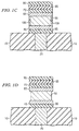
- the remaining layers of the capacitor including the PZT layer are etched with a dry plasma etching process using the etched conductive layers as a hardmask to form patterned layers 65, 55, 45 and 35.
- damaged regions 100 are formed in the PZT layer as shown in Figure 1(C). These damage regions can cause leakage currents through the PZT layer as described above.
- the etching process can also leave damage and particles on the edges of the patterned conducting layers 95, 85, 75, 65, 45, and 35 that can also introduce leakages currents in the capacitor structure.
- the wet clean process comprises exposing the structure shown in Figure 1(C) to a solution comprising phosphoric acid (H 3 PO 4 ).
- the wet clean process comprises using a solution comprising a concentration of 85% phosphoric acid although any concentration of phosphoric acid in the solution can be used.
- the temperature of the phosphoric acid solution can be between 30°C to 65°C and more preferably at around 40°C.
- the structure shown in Figure 1(C), including the PZT layer 55, can be exposed to the phosphoric acid solution using a spray, a bath, single wafer processing tools, or any other suitable method.
- the phosphoric acid wet clean method will remove the damaged regions 100 without appreciably removing the undamaged regions of the PZT layer as shown in Figure 1(D).
- the wet clean comprising phosphoric acid will also remove any damaged regions of the conductive layers 95, 85, 75, 65, 45, and 35 as well as any particles left on the structure after the plasma etching process.
- the wet clean comprising phosphoric acid will not appreciably attack the underlying dielectric layer 10 and metal contact layer 20.
Landscapes
- Semiconductor Memories (AREA)
- Semiconductor Integrated Circuits (AREA)
Abstract
Description
Claims (10)
- A method to form integrated circuit capacitors, comprising:providing a dielectric layer;forming at least one conductive layer on said dielectric layer;forming a PZT layer on said at least one conductive layer;forming at least one conductive layer on said PZT layer;etching said PZT layer; andexposing said PZT layer to phosphoric acid.
- The method of claim 1 wherein said exposing said PZT layer to phosphoric acid comprises exposing said PZT layer to a solution comprising a concentration of 85% phosphoric acid.
- The method of claim 2 wherein said solution comprises a concentration of 85% phosphoric acid is between 30°C and 65°C.
- The method of claim 3 wherein said solution comprises a concentration of 85% phosphoric acid is around 40°C.
- A method as claimed in any preceding claim, comprising:the further step of forming a plurality of conductive layers on said dielectric layer;and forming said PZT layer on said plurality.
- A method as claimed in any preceding claim comprising the further step of forming a plurality of conductive layers on said PZT layer.
- A method as claimed in any preceding claim comprising the further step of etching said conductive layer or layers.
- The method of any preceding claim wherein a conductive layer comprises iridium, titanium aluminium nitride or titanium oxynitride.
- A capacitor fabricated in accordance with the method of any preceding claim.
- A semi-conductor device including a capacitor as claimed in claim 9.
Applications Claiming Priority (2)
| Application Number | Priority Date | Filing Date | Title |
|---|---|---|---|
| US374858 | 2003-02-24 | ||
| US10/374,858 US20040166678A1 (en) | 2003-02-24 | 2003-02-24 | Wet clean method for PZT capacitors |
Publications (2)
| Publication Number | Publication Date |
|---|---|
| EP1450397A2 true EP1450397A2 (en) | 2004-08-25 |
| EP1450397A3 EP1450397A3 (en) | 2009-02-18 |
Family
ID=32736491
Family Applications (1)
| Application Number | Title | Priority Date | Filing Date |
|---|---|---|---|
| EP04100724A Withdrawn EP1450397A3 (en) | 2003-02-24 | 2004-02-24 | Wet Clean method PZT Capacitors |
Country Status (3)
| Country | Link |
|---|---|
| US (1) | US20040166678A1 (en) |
| EP (1) | EP1450397A3 (en) |
| JP (1) | JP2004260177A (en) |
Cited By (1)
| Publication number | Priority date | Publication date | Assignee | Title |
|---|---|---|---|---|
| CN111211092A (en) * | 2018-11-22 | 2020-05-29 | 中芯国际集成电路制造(北京)有限公司 | Semiconductor structure and forming method thereof |
Families Citing this family (3)
| Publication number | Priority date | Publication date | Assignee | Title |
|---|---|---|---|---|
| KR100480636B1 (en) * | 2002-11-22 | 2005-03-31 | 삼성전자주식회사 | Method for manufacturing semiconductor device |
| JP4861627B2 (en) * | 2005-01-25 | 2012-01-25 | ラピスセミコンダクタ株式会社 | Method for manufacturing ferroelectric capacitor |
| KR100685735B1 (en) * | 2005-08-11 | 2007-02-26 | 삼성전자주식회사 | Polysilicon removal composition, polysilicon removal method using the same and manufacturing method of semiconductor device |
Family Cites Families (5)
| Publication number | Priority date | Publication date | Assignee | Title |
|---|---|---|---|---|
| DE69317141T2 (en) * | 1992-04-20 | 1998-06-25 | Texas Instruments Inc | Anisotropic etching of metal oxide |
| US5439840A (en) * | 1993-08-02 | 1995-08-08 | Motorola, Inc. | Method of forming a nonvolatile random access memory capacitor cell having a metal-oxide dielectric |
| JP3122579B2 (en) * | 1994-07-27 | 2001-01-09 | シャープ株式会社 | Pt film etching method |
| US6379577B2 (en) * | 1999-06-10 | 2002-04-30 | International Business Machines Corporation | Hydrogen peroxide and acid etchant for a wet etch process |
| JP3951540B2 (en) * | 2000-02-25 | 2007-08-01 | 富士通株式会社 | Manufacturing method of semiconductor device having ferroelectric film |
-
2003
- 2003-02-24 US US10/374,858 patent/US20040166678A1/en not_active Abandoned
-
2004
- 2004-02-23 JP JP2004045590A patent/JP2004260177A/en active Pending
- 2004-02-24 EP EP04100724A patent/EP1450397A3/en not_active Withdrawn
Cited By (2)
| Publication number | Priority date | Publication date | Assignee | Title |
|---|---|---|---|---|
| CN111211092A (en) * | 2018-11-22 | 2020-05-29 | 中芯国际集成电路制造(北京)有限公司 | Semiconductor structure and forming method thereof |
| CN111211092B (en) * | 2018-11-22 | 2023-02-17 | 中芯国际集成电路制造(北京)有限公司 | Semiconductor structure and forming method thereof |
Also Published As
| Publication number | Publication date |
|---|---|
| JP2004260177A (en) | 2004-09-16 |
| US20040166678A1 (en) | 2004-08-26 |
| EP1450397A3 (en) | 2009-02-18 |
Similar Documents
| Publication | Publication Date | Title |
|---|---|---|
| US5416042A (en) | Method of fabricating storage capacitors using high dielectric constant materials | |
| US9679960B2 (en) | Semiconductor devices, methods of manufacture thereof, and methods of manufacturing capacitors | |
| US20150171098A1 (en) | Metal floating gate composite 3d nand memory devices and associated methods | |
| US7468323B2 (en) | Method of forming high aspect ratio structures | |
| US20040084400A1 (en) | Patterning metal stack layers of magnetic switching device, utilizing a bilayer metal hardmask | |
| US7221013B2 (en) | Semiconductor device | |
| KR100574678B1 (en) | Semiconductor device and manufacturing method | |
| CN108962824B (en) | Semiconductor element and manufacturing method thereof | |
| KR100880109B1 (en) | Pollution Control Method for Fabrication of Embedded Ferroelectric Devices | |
| KR100360592B1 (en) | Semiconductor devic and method for fabricating it | |
| US6329232B1 (en) | Method of manufacturing a semiconductor device | |
| US20090258469A1 (en) | Method of manufacturing semiconductor device | |
| US20040166678A1 (en) | Wet clean method for PZT capacitors | |
| JP2000196031A (en) | Capacitor and manufacturing method thereof | |
| US6297526B1 (en) | Process for producing barrier-free semiconductor memory configurations | |
| KR100533973B1 (en) | Method for forming ferroelectric capacitor capable of improving adhesion between bottom electrode and ferroelectric layer | |
| CN108933192A (en) | The production method of magnetic memory device | |
| JP3166747B2 (en) | Method for manufacturing capacitor and capacitor | |
| US6060367A (en) | Method of forming capacitors | |
| KR100390833B1 (en) | A method for forming capacitor in semiconductor device | |
| US6365328B1 (en) | Semiconductor structure and manufacturing method | |
| US20060166379A1 (en) | Method for manufacturing ferroelectric capacitor | |
| JPH05121758A (en) | Semiconductor memory element and manufacture thereof | |
| KR100278918B1 (en) | Capacitor Manufacturing Method of Semiconductor Device | |
| US20030224536A1 (en) | Contact formation |
Legal Events
| Date | Code | Title | Description |
|---|---|---|---|
| PUAI | Public reference made under article 153(3) epc to a published international application that has entered the european phase |
Free format text: ORIGINAL CODE: 0009012 |
|
| AK | Designated contracting states |
Kind code of ref document: A2 Designated state(s): AT BE BG CH CY CZ DE DK EE ES FI FR GB GR HU IE IT LI LU MC NL PT RO SE SI SK TR |
|
| AX | Request for extension of the european patent |
Extension state: AL LT LV MK |
|
| PUAL | Search report despatched |
Free format text: ORIGINAL CODE: 0009013 |
|
| AK | Designated contracting states |
Kind code of ref document: A3 Designated state(s): AT BE BG CH CY CZ DE DK EE ES FI FR GB GR HU IE IT LI LU MC NL PT RO SE SI SK TR |
|
| AX | Request for extension of the european patent |
Extension state: AL LT LV MK |
|
| 17P | Request for examination filed |
Effective date: 20090818 |
|
| 17Q | First examination report despatched |
Effective date: 20090921 |
|
| AKX | Designation fees paid |
Designated state(s): DE FR GB |
|
| STAA | Information on the status of an ep patent application or granted ep patent |
Free format text: STATUS: THE APPLICATION IS DEEMED TO BE WITHDRAWN |
|
| 18D | Application deemed to be withdrawn |
Effective date: 20100402 |