EP1450387A2 - Method of manufacturing field emission device - Google Patents
Method of manufacturing field emission device Download PDFInfo
- Publication number
- EP1450387A2 EP1450387A2 EP04250726A EP04250726A EP1450387A2 EP 1450387 A2 EP1450387 A2 EP 1450387A2 EP 04250726 A EP04250726 A EP 04250726A EP 04250726 A EP04250726 A EP 04250726A EP 1450387 A2 EP1450387 A2 EP 1450387A2
- Authority
- EP
- European Patent Office
- Prior art keywords
- layer
- electron emission
- holes
- emitters
- sacrificial layer
- Prior art date
- Legal status (The legal status is an assumption and is not a legal conclusion. Google has not performed a legal analysis and makes no representation as to the accuracy of the status listed.)
- Granted
Links
Images





Classifications
-
- H—ELECTRICITY
- H01—ELECTRIC ELEMENTS
- H01J—ELECTRIC DISCHARGE TUBES OR DISCHARGE LAMPS
- H01J1/00—Details of electrodes, of magnetic control means, of screens, or of the mounting or spacing thereof, common to two or more basic types of discharge tubes or lamps
- H01J1/02—Main electrodes
- H01J1/30—Cold cathodes, e.g. field-emissive cathode
-
- H—ELECTRICITY
- H01—ELECTRIC ELEMENTS
- H01J—ELECTRIC DISCHARGE TUBES OR DISCHARGE LAMPS
- H01J9/00—Apparatus or processes specially adapted for the manufacture, installation, removal, maintenance of electric discharge tubes, discharge lamps, or parts thereof; Recovery of material from discharge tubes or lamps
- H01J9/02—Manufacture of electrodes or electrode systems
- H01J9/022—Manufacture of electrodes or electrode systems of cold cathodes
- H01J9/025—Manufacture of electrodes or electrode systems of cold cathodes of field emission cathodes
-
- B—PERFORMING OPERATIONS; TRANSPORTING
- B82—NANOTECHNOLOGY
- B82Y—SPECIFIC USES OR APPLICATIONS OF NANOSTRUCTURES; MEASUREMENT OR ANALYSIS OF NANOSTRUCTURES; MANUFACTURE OR TREATMENT OF NANOSTRUCTURES
- B82Y10/00—Nanotechnology for information processing, storage or transmission, e.g. quantum computing or single electron logic
-
- C—CHEMISTRY; METALLURGY
- C01—INORGANIC CHEMISTRY
- C01B—NON-METALLIC ELEMENTS; COMPOUNDS THEREOF; METALLOIDS OR COMPOUNDS THEREOF NOT COVERED BY SUBCLASS C01C
- C01B32/00—Carbon; Compounds thereof
- C01B32/05—Preparation or purification of carbon not covered by groups C01B32/15, C01B32/20, C01B32/25, C01B32/30
-
- H—ELECTRICITY
- H01—ELECTRIC ELEMENTS
- H01J—ELECTRIC DISCHARGE TUBES OR DISCHARGE LAMPS
- H01J1/00—Details of electrodes, of magnetic control means, of screens, or of the mounting or spacing thereof, common to two or more basic types of discharge tubes or lamps
- H01J1/02—Main electrodes
- H01J1/30—Cold cathodes, e.g. field-emissive cathode
- H01J1/304—Field-emissive cathodes
-
- B—PERFORMING OPERATIONS; TRANSPORTING
- B82—NANOTECHNOLOGY
- B82Y—SPECIFIC USES OR APPLICATIONS OF NANOSTRUCTURES; MEASUREMENT OR ANALYSIS OF NANOSTRUCTURES; MANUFACTURE OR TREATMENT OF NANOSTRUCTURES
- B82Y40/00—Manufacture or treatment of nanostructures
-
- H—ELECTRICITY
- H01—ELECTRIC ELEMENTS
- H01J—ELECTRIC DISCHARGE TUBES OR DISCHARGE LAMPS
- H01J2201/00—Electrodes common to discharge tubes
- H01J2201/30—Cold cathodes
- H01J2201/304—Field emission cathodes
- H01J2201/30446—Field emission cathodes characterised by the emitter material
- H01J2201/30453—Carbon types
- H01J2201/30469—Carbon nanotubes (CNTs)
Definitions
- the present invention relates to a method of manufacturing an electric field device, and more particularly, to a method of manufacturing an electric field device that can uniformly emit light having a high brightness.
- Carbon nanotubes have a small diameter and a high aspect ratio of diameter to length and thus can emit electrons even at a low voltage. Since the CNTs have excellent electron emission characteristics and are chemically and physically durable, extensive studies have been performed on the physical properties and applicability thereof. Meanwhile, spindt-type field emission devices use metal micro tips as electron emitters. The micro tips have a problem that the life span is reduced under atmospheric gas and a non-uniform electric field during emission of electrons. A low work function of an emitter is required in order to lower a driving voltage for emitting electrons, but conventional micro tips are reaching the technical limit. To overcome these problems, field emission arrays (FEAs) using the foregoing CNTs as electron emitting sources have been developed because the CNTs have a high aspect ratio and are highly durable and conductive.
- FAAs field emission arrays
- U.S. Patent No. 6,440,761 discloses an FEA using a paste mixture of electron emission materials and a method of fabricating the same.
- U.S. Patent No. 6,339,281 discloses an FEA and a method of fabricating the same, in which CNTs formed by a growth method are used as emitters. Generally, since it is easier to form emitters using a paste mixture than by a growth method, the former method is preferred.
- a cathode electrode 2 is formed on a substrate 1 formed of, for example, soda lime glass.
- the cathode electrode 2 is formed by depositing indium tin oxide ([TO) and patterning the same using a photolithography process.
- [TO indium tin oxide
- a gate insulating layer 3 is formed over the substrate 1.
- the gate insulating layer 3 has holes 3a, which expose portions of the cathode electrode 2.
- the gate insulating layer 3 can be formed using, for example, a screen printing technique.
- a gate electrode 4 is formed on the gate insulating layer 3.
- the gate electrode 4 has gate holes 4a, which correspond to the holes 3a.
- the gate electrode 4 is formed by depositing a metal and patterning the same using a thin-film forming process or a thick-film forming process. Alternatively, the gate electrode 4 may be formed by a screen printing technique using a metal paste.
- a paste-type electron emission material layer 5 is formed to cover the gate electrode 4 and fill the gate holes 4a.
- the paste-type electron emission material layer 5 is formed of photoresist and electron emission materials, such as CNTs or nanoparticles.
- the electron emission material layer 5 is exposed using a mask 6. Since the electron emission material layer 5 contains a negative photoresist, if ultraviolet (UV) rays are irradiated into the holes 3a, the photoresist in the holes 3a is cured by the exposure process.
- UV ultraviolet
- the electron emission material layer 5 is developed, thereby forming emitters 5a in the holes 3a using the remaining electron emission materials.
- the emitters 5a are completely hardened and constricted by firing the emitters 5a at a predetermined temperature, thereby becoming lower in height than the gate holes 4a.
- the above-described conventional method has the following problems. While the emitters 5a are being formed using the electron emission material layer 5, a portion of the electron emission materials is very likely to remain around the gate holes 4a. The remaining portion of the electron emission materials causes a short circuiting between the emitters 5a and the gate electrode 4, which adversely affects the field emission device. The short circuiting between the emitters 5a and the gate electrode 4 makes it impossible to uniformly emit light having a high brightness and emit electrons at a certain portion where the short circuiting occurs. These problems are caused by the photolithography process, which leads the electron emission materials to contact the gate electrode 4. Accordingly, to solve the foregoing problems, it is required to prevent the electron emission materials from contacting the gate electrode 4. For this, a lift-off process can be used.
- a sacrificial layer for lift-off is formed in a region excluding portions where emitters will be formed.
- the sacrificial layer for lift-off can prevent electron emission materials from contacting a gate electrode so as not to cause a short circuiting therebetween.
- the lift-off can prevent unnecessary materials from remaining around gate holes.
- emitters cannot be patterned using a developing solution or a lift-off solution due to a strong chemical combination of photosensitive materials of the electron emission materials with certain materials of the sacrificial layer. Therefore, when emitters are intended to be formed using the lift-off process, a chemical combination of the sacrificial layer with the electron emission materials should be prevented.
- a method of manufacturing a field emission device comprises (a) preparing a substrate structure, the substrate structure comprising a substrate, a cathode electrode formed on the substrate, a gate insulating layer formed on the cathode electrode, the gate insulating layer having holes that expose portions of the cathode electrode, and a gate electrode having gate holes that correspond to the holes, the cathode electrode, the gate insulating layer, and the gate insulating layer being sequentially stacked on the substrate; (b) forming a sacrificial layer on a surface of the substrate structure excluding the portions of the cathode electrode, which are exposed by the holes, and on inner walls of the holes; (c) forming an isolation layer on the sacrificial layer, the isolation layer for preventing electron emission materials for forming emitters from contacting the sacrificial layer; (d) forming an electron emission material layer by depositing the emission electron materials on the surface of the substrate structure where the sa
- the present invention thus provides a method of manufacturing a field emission device that uniformly emits light with high brightness.
- the method also prevents short circuiting caused by remaining electron emission materials, thus forming emitters having excellent electron emission characteristics.
- the electron emission materials can be one of carbon nanotubes and nanoparticles.
- the electron emission material layer can be formed of a conductive material.
- the conductive material is formed of Ag.
- the isolation layer can be formed of a resistive material.
- the isolation layer can be formed using one selected from the group consisting of a paste, a sol-gel, and a slurry solution.
- the electron emission material layer can be formed of a conductive material using one selected from the group consisting of a paste, a sol-gel, and a slurry solution.
- the electron emission material layer and the sacrificial layer can be formed of a photoresist.
- the isolation layer can be formed using an IPA/H 2 O solution containing polyvinyl alcohol.
- a cathode electrode 20 is formed on a substrate 10, and a gate insulating layer 30 is formed thereon.
- Well-type holes 30a having a predetermined diameter and depth are formed in the gate insulating layer 30.
- Emitters 50a are formed at bottoms of the well-type holes 30a, i.e., on portions of the cathode electrode 20, which are exposed by the well-type holes 30a.
- a typical field emission device has the above-described known structure, in which the remaining material, e.g., a resistive material, of an isolation layer that is used in the method of the present invention may or may not remain at lower portions of the emitters 50a.
- the remaining material e.g., a resistive material
- a gate electrode 40 is formed on the gate insulating layer 30.
- the gate electrode 40 includes gate holes 40a via which electrons are extracted from the emitters 50a.
- An electron emission material of the present invention contains CNTs or nanoparticles, which enable the emission of electrons by an electric field.
- the emitters 50a can be formed of particles of highly conductive metals, such as Ag and Ti, to enhance the supply of a current.
- the resistive material i.e., the remaining material of the isolation layer, remains at the lower portions of the emitters 50a as described above, the resistive material allows a current to be uniformly supplied even to emission points of the CNTs or nanoparticles, which are uniformly distributed in the emitters 50a, which are highly conductive due to the conductive metal particles.
- the resistive material is preferably formed to a predetermined thickness to effectively aid the above-described supply of the current.
- a sacrificial layer may contact emitters. Thus, a reaction of materials of the sacrificial layer on materials of the emitters is very likely to occur.
- the sacrificial layer may be formed of novolac photosensitive resin. If a solvent, e.g., Texanol, which has a strong solubility against the resin, is included in the electron emission materials, an attack against the sacrificial layer by the solvent is unavoidable.
- an isolation layer is formed on the sacrificial layer to prevent materials of the sacrificial layer from contacting the electron emission materials of the emitters 50a.
- a cathode electrode 20 is formed on a substrate 10 formed of soda lime glass.
- an ITO is deposited on the substrate 10 and patterned using a photolithography process.
- a gate insulating layer 30 is formed over the substrate 10. Holes 30a are formed in the gate insulating layer 30 such that portions of the cathode electrode 20 are exposed.
- the gate insulating layer 30 can be formed by a screen printing technique or other various known methods including deposition and patterning of an insulating material.
- a gate electrode 40 is formed on the gate insulating layer 30. Gate holes 40a are formed in the gate electrode 40 so as to correspond to the holes 30a.
- the gate electrode 40 can be formed by a thin-film forming process including deposition and patterning of a metal material or a thick-film forming process including a screen printing technique using a metal paste.
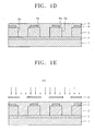
- a sacrificial layer 60 for lift-off is formed on a surface of the gate electrode 40 and inner walls of the holes 30a, excluding bottoms of the holes 30a.
- the sacrificial layer 60 is formed by a screen printing technique using a paste or a spin coating method using a sol-gel or a slurry solution and soft-baked.
- an isolation layer 70 is formed on the sacrificial layer 60.
- the isolation layer 70 is formed by a screen printing technique using a paste or a spin coating method using a sol-gel or a slurry solution and soft-baked.
- the isolation layer 70 should be formed of a material that does not react on the sacrificial layer 60 or hardly reacts thereon so as not to hinder the entire manufacturing process. Also, the isolation layer 70 should be formed of a material that hardly reacts on electron emission materials which will be formed on the isolation layer 70.
- the isolation layer 70 can be formed of a resistive material to form a material layer resistive to lower portions of the emitters and also may be formed of photosensitive photoresist.
- the resistive material can be at least one selected from the group consisting of SiO 2 , MgO, a-Si, and p-Si. If the isolation layer 70 does not include a resistive material but is used only to prevent electron emission materials from contacting the sacrificial layer 60, the isolation layer 70 is not formed on the bottoms of the holes 30 so as not to cover the cathode electrode 20 like the sacrificial layer 60 does.
- an electron emission material layer 50 is formed on the resultant structure using photoresist and electron emission materials, such as CNTs or nanoparticles.
- the electron emission material layer 50 can be formed of conductive particles, e.g., Ag; to enhance the supply of a current.
- This electron emission material layer 50 can be formed by a screen printing technique using a paste or a spin coating method using a sol-gel or a slurry solution.
- the sacrificial layer 60 and the electron emission material layer 50 are cured by heating or using ultraviolet (UV) rays.
- UV ultraviolet
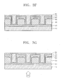
- a lift-off process for removing the sacrificial layer 60 using an etchant is performed, thereby forming preliminary emitters 50a only in the center of the bottoms of the holes 30a.
- the preliminary emitters 50a are comprised of the remaining portion of the isolation layer 70 and the electron emission material layer 50.
- the emitters 50a are fired at a predetermined temperature and completely hardened and constricted.
- the tops of the emitters 50a become lower in height than the gate holes 40a.
- pyrolytic ingredients are completely removed from the remaining isolation layer 70, and the resistive material remains to a very small thickness.
- an isolation layer is interposed between a sacrificial layer and an electron emission material layer, thereby preventing the sacrificial layer formed of a photoresist from reacting on the electron emission material layer.
- a tight combination can be prevented between the sacrificial layer and the electron emission material layer so as to facilitate a lift-off process for forming emitters.
- the resistive material layer allows a current to be uniformly supplied to a highly conductive electron emission material layer.
- the emitters can have uniform electron emission characteristics.
- FIGs. 4A and 4B are photographs showing electron emission of a field emission device manufactured by a conventional method comprising a screen printing method and a photolithography process and using neither a sacrificial layer nor an isolation layer.
- FIG. 4A shows screen brightness in conditions of an anode voltage of 1 KV, a gate voltage of 55 V, and an electron emission current of 367.5 ⁇ A
- FIG. 4B shows screen brightness in conditions of an anode voltage of 1 KV, a gate voltage of 50 V, and an electron emission voltage of 58.6 ⁇ A.
- FIGs. 5A and 5B are photographs showing electron emission of a field emission device manufactured by the method according to the present invention.
- FIG. 5A shows screen brightness in conditions of an anode voltage of 1 KV, a gate voltage of 55 V, and an electron emission current of 1.13 mA
- FIG. 5B shows screen brightness in conditions of an anode voltage of 1 KV, a gate voltage of 60 V, and an electron emission current of 2 mA.
- the field emission device manufactured by the conventional method has a lower electron emission current than that manufactured by the present invention and is very likely to emit little electrons.
- the field emission device of the present invention can solve a short circuiting, has a very high electron emission current, and ensures uniform brightness.
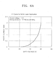
- FIG. 6A is a graph showing a relationship between anode current and gate voltage of the field emission device manufactured by the method of the present invention
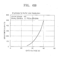
- FIG. 6B is a graph showing a relationship between brightness and gate voltage thereof.
- the field emission device manufactured by the present invention shows a very high current and brightness. Since the result of FIG. 6B is obtained when a light emission surface remains spaced about 6 cm from a sensor, it is assumed that the brightness of the field emission device for practical use is higher than the result of FIG. 6.
- a field emission device having a very high current and brightness can be obtained. Also, a lift-off process is effectively performed using an isolation layer such that a short circuiting between a gate electrode and emitters is prevented. Thus, an improved electron emission device can be obtained.
- a resistive material that remains at the lower portions of an electron emission material layer allows a current to be uniformly supplied even to emission points of CNTs or nanoparticles, which are uniformly distributed in the highly conductive electron emission material layer. Thus, electrons can be uniformly emitted throughout the entire electron emission material layer. Consequently, the life span of the field emission device can be highly increased.
- the field emission device of the present invention can be applied to devices requiring emission of electrons, for example, display devices. While the present invention has been particularly shown and described with reference to preferred embodiments thereof, it will be understood by those of ordinary skill in the art that various changes in form and details may be made therein without departing from the scope of the present invention as defined by the following claims.
Landscapes
- Engineering & Computer Science (AREA)
- Chemical & Material Sciences (AREA)
- Nanotechnology (AREA)
- Manufacturing & Machinery (AREA)
- Organic Chemistry (AREA)
- Physics & Mathematics (AREA)
- Mathematical Physics (AREA)
- Theoretical Computer Science (AREA)
- Crystallography & Structural Chemistry (AREA)
- Inorganic Chemistry (AREA)
- Cold Cathode And The Manufacture (AREA)
Abstract
Description
Claims (10)
- A method of manufacturing a field emission device, the method comprising:(a) preparing a substrate structure, the substrate structure comprising a substrate, a cathode electrode formed on the substrate, a gate insulating layer formed on the cathode electrode, the gate insulating layer having holes that expose portions of the cathode electrode, and a gate electrode having gate holes that correspond to the holes, the cathode electrode, the gate insulating layer, and the gate insulating layer being sequentially stacked on the substrate;(b) forming a sacrificial layer on a surface of the substrate structure excluding the portions of the cathode electrode, which are exposed by the holes, and on inner walls of the holes;(c) forming an isolation layer on the sacrificial layer, the isolation layer for preventing electron emission materials for forming emitters from contacting the sacrificial layer;(d) forming an electron emission material layer by depositing the emission electron materials on the surface of the substrate structure where the sacrificial layer is formed, the electron emission material layer filling the holes;(e) removing the isolation layer and the electron emission materials, which are formed on the sacrificial layer, and forming the emitters inside the holes using the electron emission material layer by performing a lift-off process using an etchant, the lift-off process for removing the sacrificial layer that is formed on the surface of the gate electrode and the inner walls of the holes; and(f) firing the emitters.
- The method of claim 1, wherein the electron emission materials are one of carbon nanotubes and nanoparticles.
- The method of claim 1, wherein the electron emission material layer and the sacrificial layer are formed of a photoresist.
- The method of claim 1, wherein the electron emission material layer is formed of a conductive material.
- The method of claim 4, wherein the electron emission material layer is selected from the group consisting of a paste, a sol-gel, and a slurry solution.
- The method of claim 4 or 5, wherein the conductive material is formed of Ag.
- The method of any preceding claim, wherein the isolation layer is formed of a resistive material.
- The method of claim 7, wherein the resistive material is formed of one selected from the group consisting of SiO2, MgO, a-Si, and p-Si.
- The method of any one of claims 1 to 6, wherein the isolation layer is formed using one selected from the group consisting of a paste, a sol-gel, and a slurry solution.
- The method of any one of claims 1 to 6, wherein the isolation layer is formed using an IPA/H2O solution containing polyvinyl alcohol.
Applications Claiming Priority (2)
| Application Number | Priority Date | Filing Date | Title |
|---|---|---|---|
| KR10-2003-0008762A KR100513727B1 (en) | 2003-02-12 | 2003-02-12 | Manufacturing method of a field emission device |
| KR2003008762 | 2003-02-12 |
Publications (3)
| Publication Number | Publication Date |
|---|---|
| EP1450387A2 true EP1450387A2 (en) | 2004-08-25 |
| EP1450387A3 EP1450387A3 (en) | 2005-02-23 |
| EP1450387B1 EP1450387B1 (en) | 2008-01-09 |
Family
ID=32733141
Family Applications (1)
| Application Number | Title | Priority Date | Filing Date |
|---|---|---|---|
| EP04250726A Expired - Lifetime EP1450387B1 (en) | 2003-02-12 | 2004-02-11 | Method of manufacturing field emission device |
Country Status (6)
| Country | Link |
|---|---|
| US (1) | US6815238B2 (en) |
| EP (1) | EP1450387B1 (en) |
| JP (1) | JP4469188B2 (en) |
| KR (1) | KR100513727B1 (en) |
| CN (1) | CN100547713C (en) |
| DE (1) | DE602004011127T2 (en) |
Families Citing this family (4)
| Publication number | Priority date | Publication date | Assignee | Title |
|---|---|---|---|---|
| US7044822B2 (en) * | 2002-12-20 | 2006-05-16 | Samsung Sdi Co., Ltd. | Method of manufacturing a field emission device utilizing the sacrificial layer |
| KR100723429B1 (en) * | 2006-07-31 | 2007-05-30 | 삼성전자주식회사 | Manufacturing Method of Gas Sensor Using Metal Ligand and Carbon Nanotube |
| KR100754410B1 (en) * | 2006-08-31 | 2007-08-31 | 삼성전자주식회사 | Manufacturing method of gas sensor |
| ITMI20071262A1 (en) * | 2007-06-22 | 2008-12-23 | Eni Spa | METHOD FOR THE IDENTIFICATION OF OXIDIZING PROPANE BACTERIA |
Family Cites Families (9)
| Publication number | Priority date | Publication date | Assignee | Title |
|---|---|---|---|---|
| US6710539B2 (en) * | 1998-09-02 | 2004-03-23 | Micron Technology, Inc. | Field emission devices having structure for reduced emitter tip to gate spacing |
| KR20000074609A (en) * | 1999-05-24 | 2000-12-15 | 김순택 | Carbon nano tube field emission array and fabricating method thereof |
| KR20010011136A (en) * | 1999-07-26 | 2001-02-15 | 정선종 | Structure of a triode-type field emitter using nanostructures and method for fabricating the same |
| US6741019B1 (en) * | 1999-10-18 | 2004-05-25 | Agere Systems, Inc. | Article comprising aligned nanowires |
| KR100480773B1 (en) * | 2000-01-07 | 2005-04-06 | 삼성에스디아이 주식회사 | Method for fabricating triode-structure carbon nanotube field emitter array |
| US6682383B2 (en) * | 2000-05-17 | 2004-01-27 | Electronics And Telecommunications Research Institute | Cathode structure for field emission device and method of fabricating the same |
| US6440763B1 (en) * | 2001-03-22 | 2002-08-27 | The United States Of America As Represented By The Secretary Of The Navy | Methods for manufacture of self-aligned integrally gated nanofilament field emitter cell and array |
| JP2003016954A (en) * | 2001-04-25 | 2003-01-17 | Sony Corp | Electron emission device and its manufacturing method, cold cathode field emission device and its manufacturing method, and cold cathode field emission display device and its manufacturing method |
| US6703252B2 (en) * | 2002-01-31 | 2004-03-09 | Hewlett-Packard Development Company, L.P. | Method of manufacturing an emitter |
-
2003
- 2003-02-12 KR KR10-2003-0008762A patent/KR100513727B1/en not_active Expired - Fee Related
-
2004
- 2004-02-11 EP EP04250726A patent/EP1450387B1/en not_active Expired - Lifetime
- 2004-02-11 DE DE602004011127T patent/DE602004011127T2/en not_active Expired - Lifetime
- 2004-02-12 CN CNB2004100352789A patent/CN100547713C/en not_active Expired - Fee Related
- 2004-02-12 US US10/776,511 patent/US6815238B2/en not_active Expired - Fee Related
- 2004-02-12 JP JP2004035195A patent/JP4469188B2/en not_active Expired - Lifetime
Also Published As
| Publication number | Publication date |
|---|---|
| CN100547713C (en) | 2009-10-07 |
| EP1450387B1 (en) | 2008-01-09 |
| JP4469188B2 (en) | 2010-05-26 |
| KR100513727B1 (en) | 2005-09-08 |
| DE602004011127D1 (en) | 2008-02-21 |
| KR20040072321A (en) | 2004-08-18 |
| US20040161867A1 (en) | 2004-08-19 |
| EP1450387A3 (en) | 2005-02-23 |
| US6815238B2 (en) | 2004-11-09 |
| JP2004247306A (en) | 2004-09-02 |
| CN1530997A (en) | 2004-09-22 |
| DE602004011127T2 (en) | 2009-01-02 |
Similar Documents
| Publication | Publication Date | Title |
|---|---|---|
| EP1221710B1 (en) | Method of manufacturing triode carbon nanotube field emitter array | |
| CN100487847C (en) | Field emitting display of electronic emitting source including forming multilayer structure | |
| CN1182562C (en) | field emission device | |
| CN100501498C (en) | Field emission device and method for forming field emission device | |
| US7137860B2 (en) | Method for fabricating a field emission display with carbon-based emitter | |
| US20040036401A1 (en) | Field electron emission apparatus and method for manufacturing the same | |
| KR101009983B1 (en) | Electron emission display device | |
| US7413763B2 (en) | Method of fabricating carbon nanotube field emission source | |
| EP1450387B1 (en) | Method of manufacturing field emission device | |
| US8269210B2 (en) | Cathode assembly containing an ultraviolet light-blocking dielectric layer | |
| US7044822B2 (en) | Method of manufacturing a field emission device utilizing the sacrificial layer | |
| CN1737984B (en) | Field emission device and field emission display using same | |
| KR100805318B1 (en) | Method of manufacturing field emission display device having emitter formed of carbon-based material | |
| KR20050115057A (en) | A long life-time field emitter for a field emission device and a method for fabricating the same | |
| KR100519762B1 (en) | Manufacturing methode of field emission device | |
| KR20010104960A (en) | Cathode for field emission device and its fabrication method | |
| JP4649739B2 (en) | Method for manufacturing cold cathode field emission device | |
| KR101166014B1 (en) | A composition for preparing an electron emitter, the electron emitter prepared using the composition, and an electron emission device comprising the electron emitter | |
| KR100303546B1 (en) | Field emission display and manufacturing method of the same | |
| JP2000195448A (en) | Flat display device and method of manufacturing field emission type cathode | |
| TW200931473A (en) | Cathode planes for field emission | |
| KR20050051308A (en) | Field emission display device and manufacturing method of the same | |
| JPH0670893B2 (en) | Phosphor screen forming method in phosphor dot array tube | |
| KR20050096524A (en) | Electron emission device having layer for preventing diffusion of auxiliary electrode and method for forming the same | |
| KR20010001391A (en) | Method of Fabricating Focusing Device in Field Emission Display |
Legal Events
| Date | Code | Title | Description |
|---|---|---|---|
| PUAI | Public reference made under article 153(3) epc to a published international application that has entered the european phase |
Free format text: ORIGINAL CODE: 0009012 |
|
| AK | Designated contracting states |
Kind code of ref document: A2 Designated state(s): AT BE BG CH CY CZ DE DK EE ES FI FR GB GR HU IE IT LI LU MC NL PT RO SE SI SK TR |
|
| AX | Request for extension of the european patent |
Extension state: AL LT LV MK |
|
| RIN1 | Information on inventor provided before grant (corrected) |
Inventor name: LEE, HANG-WOO Inventor name: LEE, JEONG-HEE Inventor name: PARK, SHANG-HYEUN Inventor name: KIM, YOU-JONG |
|
| PUAL | Search report despatched |
Free format text: ORIGINAL CODE: 0009013 |
|
| AK | Designated contracting states |
Kind code of ref document: A3 Designated state(s): AT BE BG CH CY CZ DE DK EE ES FI FR GB GR HU IE IT LI LU MC NL PT RO SE SI SK TR |
|
| AX | Request for extension of the european patent |
Extension state: AL LT LV MK |
|
| 17P | Request for examination filed |
Effective date: 20050525 |
|
| AKX | Designation fees paid |
Designated state(s): DE FR GB |
|
| GRAP | Despatch of communication of intention to grant a patent |
Free format text: ORIGINAL CODE: EPIDOSNIGR1 |
|
| GRAS | Grant fee paid |
Free format text: ORIGINAL CODE: EPIDOSNIGR3 |
|
| GRAA | (expected) grant |
Free format text: ORIGINAL CODE: 0009210 |
|
| AK | Designated contracting states |
Kind code of ref document: B1 Designated state(s): DE FR GB |
|
| REG | Reference to a national code |
Ref country code: GB Ref legal event code: FG4D |
|
| REF | Corresponds to: |
Ref document number: 602004011127 Country of ref document: DE Date of ref document: 20080221 Kind code of ref document: P |
|
| ET | Fr: translation filed | ||
| PLBE | No opposition filed within time limit |
Free format text: ORIGINAL CODE: 0009261 |
|
| STAA | Information on the status of an ep patent application or granted ep patent |
Free format text: STATUS: NO OPPOSITION FILED WITHIN TIME LIMIT |
|
| 26N | No opposition filed |
Effective date: 20081010 |
|
| PGFP | Annual fee paid to national office [announced via postgrant information from national office to epo] |
Ref country code: DE Payment date: 20110208 Year of fee payment: 8 Ref country code: FR Payment date: 20110218 Year of fee payment: 8 |
|
| PGFP | Annual fee paid to national office [announced via postgrant information from national office to epo] |
Ref country code: GB Payment date: 20110209 Year of fee payment: 8 |
|
| GBPC | Gb: european patent ceased through non-payment of renewal fee |
Effective date: 20120211 |
|
| REG | Reference to a national code |
Ref country code: FR Ref legal event code: ST Effective date: 20121031 |
|
| REG | Reference to a national code |
Ref country code: DE Ref legal event code: R119 Ref document number: 602004011127 Country of ref document: DE Effective date: 20120901 |
|
| PG25 | Lapsed in a contracting state [announced via postgrant information from national office to epo] |
Ref country code: FR Free format text: LAPSE BECAUSE OF NON-PAYMENT OF DUE FEES Effective date: 20120229 Ref country code: GB Free format text: LAPSE BECAUSE OF NON-PAYMENT OF DUE FEES Effective date: 20120211 |
|
| PG25 | Lapsed in a contracting state [announced via postgrant information from national office to epo] |
Ref country code: DE Free format text: LAPSE BECAUSE OF NON-PAYMENT OF DUE FEES Effective date: 20120901 |