EP1447890A1 - Variable reflectance laser cavity mirror - Google Patents
Variable reflectance laser cavity mirror Download PDFInfo
- Publication number
- EP1447890A1 EP1447890A1 EP03028972A EP03028972A EP1447890A1 EP 1447890 A1 EP1447890 A1 EP 1447890A1 EP 03028972 A EP03028972 A EP 03028972A EP 03028972 A EP03028972 A EP 03028972A EP 1447890 A1 EP1447890 A1 EP 1447890A1
- Authority
- EP
- European Patent Office
- Prior art keywords
- mirror
- pockels cell
- electrically controlled
- recited
- retardation
- Prior art date
- Legal status (The legal status is an assumption and is not a legal conclusion. Google has not performed a legal analysis and makes no representation as to the accuracy of the status listed.)
- Withdrawn
Links
- 239000007787 solid Substances 0.000 claims abstract description 28
- 239000013078 crystal Substances 0.000 claims description 36
- 239000002131 composite material Substances 0.000 claims description 3
- 238000002310 reflectometry Methods 0.000 abstract description 26
- 230000003068 static effect Effects 0.000 description 7
- 230000010287 polarization Effects 0.000 description 5
- 238000007493 shaping process Methods 0.000 description 4
- JNDMLEXHDPKVFC-UHFFFAOYSA-N aluminum;oxygen(2-);yttrium(3+) Chemical compound [O-2].[O-2].[O-2].[Al+3].[Y+3] JNDMLEXHDPKVFC-UHFFFAOYSA-N 0.000 description 3
- 238000003491 array Methods 0.000 description 3
- 229910019901 yttrium aluminum garnet Inorganic materials 0.000 description 3
- 230000000295 complement effect Effects 0.000 description 2
- 238000005094 computer simulation Methods 0.000 description 2
- 230000005684 electric field Effects 0.000 description 2
- 239000000463 material Substances 0.000 description 2
- 230000003287 optical effect Effects 0.000 description 2
- 239000000758 substrate Substances 0.000 description 2
- 239000000853 adhesive Substances 0.000 description 1
- 230000001070 adhesive effect Effects 0.000 description 1
- 230000005540 biological transmission Effects 0.000 description 1
- 239000004020 conductor Substances 0.000 description 1
- 238000000151 deposition Methods 0.000 description 1
- 230000000694 effects Effects 0.000 description 1
- PCHJSUWPFVWCPO-UHFFFAOYSA-N gold Chemical compound [Au] PCHJSUWPFVWCPO-UHFFFAOYSA-N 0.000 description 1
- 239000010931 gold Substances 0.000 description 1
- 229910052737 gold Inorganic materials 0.000 description 1
- 230000000873 masking effect Effects 0.000 description 1
- 238000005086 pumping Methods 0.000 description 1
- 229910052761 rare earth metal Inorganic materials 0.000 description 1
- 150000002910 rare earth metals Chemical class 0.000 description 1
- 239000004065 semiconductor Substances 0.000 description 1
Images


Classifications
-
- G—PHYSICS
- G02—OPTICS
- G02F—OPTICAL DEVICES OR ARRANGEMENTS FOR THE CONTROL OF LIGHT BY MODIFICATION OF THE OPTICAL PROPERTIES OF THE MEDIA OF THE ELEMENTS INVOLVED THEREIN; NON-LINEAR OPTICS; FREQUENCY-CHANGING OF LIGHT; OPTICAL LOGIC ELEMENTS; OPTICAL ANALOGUE/DIGITAL CONVERTERS
- G02F1/00—Devices or arrangements for the control of the intensity, colour, phase, polarisation or direction of light arriving from an independent light source, e.g. switching, gating or modulating; Non-linear optics
- G02F1/01—Devices or arrangements for the control of the intensity, colour, phase, polarisation or direction of light arriving from an independent light source, e.g. switching, gating or modulating; Non-linear optics for the control of the intensity, phase, polarisation or colour
- G02F1/03—Devices or arrangements for the control of the intensity, colour, phase, polarisation or direction of light arriving from an independent light source, e.g. switching, gating or modulating; Non-linear optics for the control of the intensity, phase, polarisation or colour based on ceramics or electro-optical crystals, e.g. exhibiting Pockels effect or Kerr effect
- G02F1/0305—Constructional arrangements
- G02F1/0311—Structural association of optical elements, e.g. lenses, polarizers, phase plates, with the crystal
-
- G—PHYSICS
- G02—OPTICS
- G02F—OPTICAL DEVICES OR ARRANGEMENTS FOR THE CONTROL OF LIGHT BY MODIFICATION OF THE OPTICAL PROPERTIES OF THE MEDIA OF THE ELEMENTS INVOLVED THEREIN; NON-LINEAR OPTICS; FREQUENCY-CHANGING OF LIGHT; OPTICAL LOGIC ELEMENTS; OPTICAL ANALOGUE/DIGITAL CONVERTERS
- G02F2202/00—Materials and properties
- G02F2202/40—Materials having a particular birefringence, retardation
-
- G—PHYSICS
- G02—OPTICS
- G02F—OPTICAL DEVICES OR ARRANGEMENTS FOR THE CONTROL OF LIGHT BY MODIFICATION OF THE OPTICAL PROPERTIES OF THE MEDIA OF THE ELEMENTS INVOLVED THEREIN; NON-LINEAR OPTICS; FREQUENCY-CHANGING OF LIGHT; OPTICAL LOGIC ELEMENTS; OPTICAL ANALOGUE/DIGITAL CONVERTERS
- G02F2203/00—Function characteristic
- G02F2203/02—Function characteristic reflective
-
- G—PHYSICS
- G02—OPTICS
- G02F—OPTICAL DEVICES OR ARRANGEMENTS FOR THE CONTROL OF LIGHT BY MODIFICATION OF THE OPTICAL PROPERTIES OF THE MEDIA OF THE ELEMENTS INVOLVED THEREIN; NON-LINEAR OPTICS; FREQUENCY-CHANGING OF LIGHT; OPTICAL LOGIC ELEMENTS; OPTICAL ANALOGUE/DIGITAL CONVERTERS
- G02F2203/00—Function characteristic
- G02F2203/07—Polarisation dependent
-
- H—ELECTRICITY
- H01—ELECTRIC ELEMENTS
- H01S—DEVICES USING THE PROCESS OF LIGHT AMPLIFICATION BY STIMULATED EMISSION OF RADIATION [LASER] TO AMPLIFY OR GENERATE LIGHT; DEVICES USING STIMULATED EMISSION OF ELECTROMAGNETIC RADIATION IN WAVE RANGES OTHER THAN OPTICAL
- H01S3/00—Lasers, i.e. devices using stimulated emission of electromagnetic radiation in the infrared, visible or ultraviolet wave range
- H01S3/10—Controlling the intensity, frequency, phase, polarisation or direction of the emitted radiation, e.g. switching, gating, modulating or demodulating
- H01S3/105—Controlling the intensity, frequency, phase, polarisation or direction of the emitted radiation, e.g. switching, gating, modulating or demodulating by controlling the mutual position or the reflecting properties of the reflectors of the cavity, e.g. by controlling the cavity length
-
- H—ELECTRICITY
- H01—ELECTRIC ELEMENTS
- H01S—DEVICES USING THE PROCESS OF LIGHT AMPLIFICATION BY STIMULATED EMISSION OF RADIATION [LASER] TO AMPLIFY OR GENERATE LIGHT; DEVICES USING STIMULATED EMISSION OF ELECTROMAGNETIC RADIATION IN WAVE RANGES OTHER THAN OPTICAL
- H01S3/00—Lasers, i.e. devices using stimulated emission of electromagnetic radiation in the infrared, visible or ultraviolet wave range
- H01S3/10—Controlling the intensity, frequency, phase, polarisation or direction of the emitted radiation, e.g. switching, gating, modulating or demodulating
- H01S3/106—Controlling the intensity, frequency, phase, polarisation or direction of the emitted radiation, e.g. switching, gating, modulating or demodulating by controlling devices placed within the cavity
- H01S3/107—Controlling the intensity, frequency, phase, polarisation or direction of the emitted radiation, e.g. switching, gating, modulating or demodulating by controlling devices placed within the cavity using electro-optic devices, e.g. exhibiting Pockels or Kerr effect
-
- H—ELECTRICITY
- H01—ELECTRIC ELEMENTS
- H01S—DEVICES USING THE PROCESS OF LIGHT AMPLIFICATION BY STIMULATED EMISSION OF RADIATION [LASER] TO AMPLIFY OR GENERATE LIGHT; DEVICES USING STIMULATED EMISSION OF ELECTROMAGNETIC RADIATION IN WAVE RANGES OTHER THAN OPTICAL
- H01S3/00—Lasers, i.e. devices using stimulated emission of electromagnetic radiation in the infrared, visible or ultraviolet wave range
- H01S3/10—Controlling the intensity, frequency, phase, polarisation or direction of the emitted radiation, e.g. switching, gating, modulating or demodulating
- H01S3/11—Mode locking; Q-switching; Other giant-pulse techniques, e.g. cavity dumping
- H01S3/1103—Cavity dumping
Definitions
- the present invention relates to a variable reflectance mirror and more particularly to an electrically controlled variable reflectance electro-optic mirror suitable for use as an outcoupling mirror, for example, in a solid state lasing system, which enables the output of the lasing system to be controlled electronically and thus remotely to enable the solid state lasing system to be used in a relatively wide range of operating conditions with a single set of optics.
- Solid state lasing systems are generally known in the art. Examples of such solid state lasing systems are disclosed in U.S. Patent Nos. 5,555,254; 5,646,773; 6,094,297 and 6,178,040. Such solid state lasing systems normally include an elongated slab of a solid state lasing material, for example, a rare earth doped yttrium-aluminum-garnet (YAG) crystal and one or more diode arrays for exciting the solid state lasing material to a relatively high metastable state. Exemplary diode arrays for pumping such solid state lasing systems are disclosed in U.S. Patent Nos. 5,317,585; 5,351,251 and 6,208,677. Such solid state lasing systems also include a total reflectivity resonator mirror and an outcoupling mirror.
- YAG yttrium-aluminum-garnet
- variable reflective mirror systems are known to be formed from a static waveplate and a polarizer, as disclosed in "Solid State Laser Engineering”, by Walter Koechner, 2 nd Edition, published by Springer-Verlag, page 201, copyright 1988.
- Such variable reflectance mirrors are also known to be formed from static birefringence elements and a polarizer as disclosed in "Solid State Engineering” by Walter Koechner, 2 nd edition, published by Springer-Verlag, page 239, copyright 1988 and "Lasers", by Siegman, published by University Science Books, page 921, copyright 1986.
- variable reflectivity mirrors are also discussed in detail in "Lasers” by Siegman, published by University Science Books, pages 913-922, copyright 1986 and U.S. Patent Nos. 4,575,849; 5,260,964; 5,299,220 and 5,260,964.
- U.S. Patent No. 5,75,849 discloses a spatially varying optical filter which includes a spatially varying static birefringence element and a polarizer.
- U.S. Patent No. 5,260,964 discloses a static graded reflectivity mirror formed from a partial reflector configured such that the reflectivity varies gradually as a function of the position on the mirror surface.
- U.S. Patent No. 5,299,220 discloses a use of a one-dimensional static graded reflectivity mirror.
- Electrically operated mirrors have been developed, used primarily in the automotive industry, to provide automatic reflectance control of rearview and side view mirrors as a function of ambient light intensity. Examples of such electrically controlled mirrors, also known as electrochromic mirrors, are disclosed in U.S. Patent Nos. 5,066,112; 5,808,778 and 5,812,321. Unfortunately, such mirrors are unsuitable for use in lasing systems.
- U.S. Patent No. 6,041,071 discloses a variable reflectance mirror that is controlled electrically to enable the wavelength of a semiconductor laser system to be controlled externally.
- the electrically controlled variable reflectance mirror disclosed in the '071 patent is formed from a ferro-electric electro-optical substrate and a distributed Bragg reflector.
- An external voltage applied to the ferro-electric electro-optical substrate controls the strain and thus the characteristics of the distributed Bragg reflector to enable the wavelength of the output beams passing through the outcoupling mirror to be electrically controlled.
- Unfortunately such a system is not suitable for electrically controlling other characteristics, such as the output power of a lasing system. Accordingly, there is a need for an outcoupling mirror system whose reflectivity can be electrically controlled to enable a lasing system to be used with different operating conditions with a single set of optics.
- the electrically controlled variable reflectance mirror includes a Pockels cell which enables the light outcoupled from a laser cavity to be controlled by controlling the retardation or birefringence. Since the retardation is a function of the voltage applied to the Pockels cell, the voltage can be used to control the fraction of the output beam that is outcoupled from the laser cavity.
- the Pockels cell is formed with a constant reflectivity profile to form an electrically controlled uniform reflectivity electro-optic mirror.
- the Pockels cell is configured with spatially varying retardation to form an electrically controlled graded reflectivity electro-optic mirror. Both embodiments of the invention enable a lasing system, such as a solid state lasing system, to be operated over a relatively wide range of operating parameters utilizing a single set of optics.
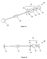
- FIG. 1A is a perspective view of a electrically controlled variable reflectance mirror in accordance with.the present invention.
- FIG. 1B is a top view of the electrically controlled variable reflectance mirror illustrated in FIG. 1A.
- FIG. 2A is a perspective view of an electrically controlled graded reflectivity mirror in accordance with the present invention.
- FIG. 2B is a top view of the electrically controlled reflectivity mirror illustrated in FIG. 2A.
- FIG. 3 is a perspective view of one embodiment of a Pockels cell formed with spatially varying retardation for use with the electrically controlled graded reflectivity mirror illustrated in FIGS. 2A and 2B.
- FIG. 4 is a perspective view of an alternate embodiment of the Pockels cell illustrated in Fig. 3 for use with the electrically controlled graded reflectivity mirror illustrated in FIGS. 2A and 2B.
- FIG. 5 is a perspective view of another alternate embodiment Pockels cell illustrated in Fig. 3 for use with the electrically controlled graded reflectivity mirror illustrated in FIGS. 2A and 2B.
- FIG. 6 is perspective view of a two-dimensional electrically controlled graded reflectivity mirror formed from two orthogonal Pockels cells in accordance with another aspect of the invention.
- FIG. 7 is perspective view of an electrically controlled spatial filter in accordance with another aspect of the invention.
- FIG. 8 is a perspective view of a Pockels cell for use in the electrically controlled spatial filter illustrated in FIG. 7.
- an electrically controlled variable reluctance mirror system for use as an outcoupling mirror, for example, in solid state lasing systems, to enable such solid state lasing systems to operate over a relatively wide range of parameters utilizing a single set of optics.
- an electrically controlled uniform reflectivity electro-optic mirror as illustrated in Figs. 1A and 1B, incorporates a standard Pockels cell.
- Such standard Pockels cells are extremely well known in the art and are disclosed in, for example, U.S. Patent Nos. 5,029,273; 5,416,620; 6,127,817 and U.S. Statutory Invention Registration H868.
- FIGS. 2A and 2B illustrate an alternate embodiment of the invention for an electrically controlled graded reflectivity electro-optic mirror.
- the electrically controlled graded reflectivity electro-optic mirror illustrated in FIGS. 2A and 2B utilizes custom Pockels cell as illustrated in FIGS. 3-5.
- FIGS. 6 illustrates another alternate embodiment of a two dimensional electrically controlled graded reflectivity mirror formed from two orthogonal Pockels cells.
- FIGS. 7 relates to yet another alternate embodiment of the invention and in particular to an electrically controlled spatial filter which utilizes a Pockels cell as illustrated in FIG. 8. All of the embodiments of the invention rely on controlling the retardation or birefringence of a Pockels cell to outcouple light from a laser cavity. Since the retardation is function of the voltage applied to Pockels cells, the voltage can be used to control the outcoupling fraction.
- the electrically controlled variable reflectance mirror 26 is illustrated in a solid state lasing system, generally identified with the reference numeral 20, which includes a totally reflecting mirror 22, which, as illustrated in FIG. 1B, is typically curved.
- the solid state lasing system 20 also includes another total reflecting mirror 24.
- the total reflecting mirror 24, for example, a flat mirror replaces the outcoupling mirror normally used in such solid state lasing systems.
- a gain medium 26 is disposed between the mirrors 22 and 24 which defines a lasing cavity.
- the gain medium 26 may be, for example, a YAG crystal pumped by a diode array (not shown) as discussed above.
- the outcoupling mirror system 26 in accordance with one aspect of the invention is formed from a standard Pockels cell 28, a 8/4 wave plate 30 and a polarizer 32, for example, a dielectric polarizer.
- the outcoupled beam is identified with the arrow 34.
- the retardation or birefringence of a Pockels cell varies as a function of the external voltage applied to the cell.
- the Pockels cell 28 acts as a passive element.
- the 8/4 waveplate 30 converts linear polarized light into circular polarized light and rotates the polarization by 90° after a round trip through it. The rotated beam is rejected from the laser cavity by the polarizer 32 forming the output beam 34.
- the Pockels cell 28 becomes active and causes a retardation which partially compensates for the retardation caused by the waveplate 30 causing the beam to be elliptically polarized.
- the elliptically polarized beam is only partially ejected by the polarizer 32 forming a partial reflector.
- the voltage on the Pockels cell 28 reaches a value that enables it to fully compensate for the waveplate 30, the rotation of the polarization caused by the waveplate 30 is fully compensated by the Pockels cell 28 which enables 100% of the beam to pass through the polarizer 32 effectively producing a total reflector.
- the electrically controlled variable reluctance mirror formed from the standard Pockels cell 28, 8/4 waveplate 30 and polarizer 32, collectively identified with the reference numeral 26, serve as an electrically controlled outcoupler with a uniform reflectivity that can vary between 0% and 100% as the voltage is varied from zero to a voltage which enables the Pockels cell to fully compensate for the 90° rotation in the polarization caused by the 8/4 waveplate 30. This voltage is called the 8/4 wave voltage.
- FIGS. 2A and 2B illustrate an alternate embodiment of the invention, shown in a solid state laser application 36, which includes a electrically controlled graduated reflectance mirror 50, for outcoupling a portion of the light beam from the laser cavity to form an output beam.
- a Pockels cell as illustrated in FIGS. 3-5, is used to introduce a spatially varying retardation to form an electrically controlled graduated reflectance mirror system as will be discussed in more detail below.
- the spatially varying retardation may be created in various ways including: shaping the electrode on a Pockels cell crystal, as generally shown in FIG. 3; shaping the Pockels cell crystal itself as shown in FIG. 5; and fabricating a composite crystal such that only a spatially varying length section of the crystal is active as illustrated in FIG. 4.
- the solid state lasing system includes a totally reflecting mirror 38, which may curved as illustrated in FIG. 2B.
- the solid state lasing system 36 also includes another totally reflecting mirror 40, which, in this case, is curved as illustrated in FIG. 2B.
- the totally reflecting mirror 40 replaces the outcoupling mirror that is typically used in such an application.
- a gain medium 42 is disposed between the mirrors 38 and 40 and defines a lasing cavity therebetween.
- the electrically controlled graduated reflectivity mirror includes a 8/4 waveplate 44, a Pockels cell 46 and polarizer 48, collectively identified with the reference numeral 50.
- the output beam is generally identified with the arrow 52.
- Various embodiments of the Pockels cell 46 are contemplated for providing spatially varying retardation.
- the various embodiments of the Pockels cell 46 are illustrated in FIGS. 3-5.
- FIG. 3 a first embodiment of a Pockels cell is shown for use with the electrically controlled graded reflectance mirror as illustrated in FIGS. 2A and 2B.
- the Pockels cell illustrated in FIG. 3 is generally identified with the reference numeral 54.
- the spatially varying retardation is formed by shaping the electrode 56 on the Pockels cell crystal.
- a Guassian retardation profile 58 is shown in Fig. 3 and described, the electrode can be configured with virtually any profile.
- the retardation or birefringence of such Pockels cells rely on an external voltage applied to the electrode 56.
- a high voltage power supply 60 is provided and coupled to the electrode 56 by way of electrical conductors 62.
- Pockels cells are formed by depositing electrodes, for example, gold electrodes, on opposing surfaces of an electro-optically active crystal, such as BBO or LiNBO 3 .
- an electro-optically active crystal such as BBO or LiNBO 3 .
- the crystal becomes birefringence and causes retardation.
- delta is the phase retardation
- 8 is the wavelength
- R is the electro-optic coefficient
- N is the index of refraction
- V is applied voltage
- L is the length of the active section of the crystal when the field is present
- d is the crystal thickness in the direction of the applied field.
- the active length of the crystal is spatially varying, the retardation will also be spatially varying.
- the crystal thickness is spatially varying, the retardation will also vary spatially.
- the active length of the crystal is tailored by having a spatially formed electrode, for example, with a Gaussian profile, formed in the x-dimension. This results in a one-dimensional graded reflectivity mirror which has 100% transmission on the top and bottom edges and a center reflectivity that can vary from 0% to 100% by varying the applied voltage.
- the geometry of the Pockels cells 54 minimizes field spreading and produces good retardation fidelity with respect to the shape of the electrode 56.
- the electrodes can be made into any shape useful for resonator design with proper masking, such as high order Gaussian profiles, flat tops or even Bessel functions.
- the Pockels cell 64 includes a composite crystal formed with an electro-optically active crystal portion 66 and an electro-optically passive crystal portion 68.
- the electrically active portion 68 is formed with an exemplary birefringence profile. Other profiles could also be used.
- the electrically active crystal portion 66 can be formed by bonding for example, with (please identify an example adhesive) two sections of crystals (IDENTITY CRYSTALS) together where the active portion 66 is crystal graphically oriented properly and the inactive portion 68 is not.
- the activity can be controlled by poling one section of the crystal opposite from the other.
- a pair of electrodes 67 are formed on the opposing sides of the active crystal portion 66. The electrodes 67 may optionally extend over the inactive portion 68.
- the retardation profile 70 for Pockels cell 64 is similar to the retardation profile 58 for the Pockels cell 54.
- the Pockels cell 64 requires a high voltage supply 72 connected to the electrodes 67 by way of a pair of high voltage connections, generally identified with reference numeral 74.
- FIG. 5 An alternate embodiment of the Pockels cell is illustrated in FIG. 5 and generally identified with the reference numeral 76.
- the performance of the Pockels cell is controlled by shaping the width or thickness of the crystal to define a profile, for example, as illustrated with the reference numeral 82.
- the electrodes are formed on the opposing surfaces 78 and 80 of the Pockels cell 76.
- a high voltage supply 84 may then be coupled to the Pockels cell 76 by way of a pair of high voltage connections; generally identified with the reference numeral 88.
- computer models may be used to define the exact crystal shape that will yield a desire spatially varying retardation profile. (PROVIDE REFERENCE)
- FIG. 6 illustrates an alternate embodiment of the invention forming a two-dimensional electrically controlled graduated reflectance mirror 106.
- the two-dimensional electrically controlled graduated reflectance mirror is illustrated in a solid state lasing system, generally identified with the reference numeral 90.
- the lasing system includes a totally reflecting mirror 92, for example, a curved mirror similar to the mirror 38 illustrated in FIG. 2B.
- the lasing system 90 also includes another totally reflective mirror 94 which also may be curved, similar to the mirror 40 illustrated in FIG. 2B.
- the mirror 94 replaces the outcoupler mirror typically used in such applications.
- a gain medium 96 is disposed between the mirrors 92 and 94 defining a laser cavity therebetween.
- the two-dimensional electrically controlled graduated reflective mirror includes a 8/4 wave retardation plate 98 which converts linearly polarized light into circular polarization and rotates the polarization by 90° after a round trip through it.
- a pair of Pockels cells 100 and 102 are provided, which incorporate Pockels cells, for example, as illustrated in FIGS. 3-5.
- the two-dimensional electrically controlled graduated reflectance mirror also includes a polarizer 104, a 8/4 waveplate 98, Pockels cells 100 and 102 and a polarizer 104, collectively identified with the reference numeral 106.
- the Pockels cells 100 and 102 may be formed from one of the Pockels cells illustrated in FIGS. 3-5 but oriented orthogonal relative to one another.
- the Pockels cell 100 may be oriented so that the spatially varying retardation is in the horizontal direction while the Pockels cell 102 is oriented so that the spatially varying retardation is in a vertical direction.
- the retardation profiles 108 and 110 for the Pockels cells 100 and 102, respectively, in this embodiment are summed to produce a two-dimensional retardation profile.
- the embodiment illustrated in FIG. 6 is suited for relatively low aspect ratio beams. Computer modeling may be used to determine the shape of the electrode such that the position of the two fields produces a desired spatial profile. Because of the low aspect ratio, field spreading is preferably taken into account. (PROVIDE REFERENCE)
- FIGS. 7 and 8 illustrate an alternate embodiment of the invention in which an electrically controlled graduated reflectance mirror can be used as an electrically controlled spatial filter. As such, it can be used with a partial reflector to control the cavity mode in a stable resonator.
- a Gaussian or higher Gaussian profile spatial filter for example, is useful in controlling the mode of a resonator without introducing a defractive loss.
- a Pockels cell is used with a retardation plate with a complementary spatial profile such that the retardation is zero at the center of the Pockels cell and increases towards the edges to 100% when 8/4 wave voltage is applied.
- the solid state lasing system 112 includes a totally reflecting mirror 114, which may be curved similar to the mirror 38 illustrated in FIG. 2B.
- the solid state lasing system 112 further includes a partially reflecting mirror 106 which is typically flat for stable resonator cavities.
- a gain medium 118 is disposed between the mirrors 114 and 116 and defines a laser cavity therebetween.
- the electrically controlled spatial filter includes a Pockels cell 120 and a polarizer 122.
- the Pockels cell 120 and polarizer 122 which form the electrically controlled spatial filter are collectively identified with the reference numeral 124.
- the Pockels cell 120 is formed with an electrode 126 having a pattern that is complementary to the electrode pattern illustrated in FIG. 3, for example, an inverse Gaussian profile.
- the retardation profile 128 for the Pockels cell 120 is illustrated in FIG. 8.
- the center where there is no electrode
- the edges will have 8/4 wave retardation.
- a high voltage power supply 130 is connected to the Pockels cell 120 by way of a pair of high voltage electrical connections 132.
- the pocket cell 120 0f Fig. 8 may of course also be used in the system according to Fig. 2 or is the system according to Fig. 6.
Landscapes
- Physics & Mathematics (AREA)
- Nonlinear Science (AREA)
- Chemical & Material Sciences (AREA)
- Engineering & Computer Science (AREA)
- Ceramic Engineering (AREA)
- Crystallography & Structural Chemistry (AREA)
- General Physics & Mathematics (AREA)
- Optics & Photonics (AREA)
- Lasers (AREA)
- Optical Modulation, Optical Deflection, Nonlinear Optics, Optical Demodulation, Optical Logic Elements (AREA)
- Semiconductor Lasers (AREA)
Abstract
An electrically controlled variable reflectance mirror (34) including a Pockels
cell (28) which enables its retardation or birefringence to be controlled in order
to vary the light outcoupled from a laser cavity. Since the retardation is a
function of the voltage applied to be Pockels cell, the voltage can be used to control the fraction
of the output beam that is outcoupled from the laser cavity. In one embodiment of the invention,
the Pockels cell (28) is formed with a constant reflectivity profile to form an electrically controlled
uniform reflectivity electro-optic mirror. In an alternate embodiment of the invention, the
Pockels cell is configured with spatially varying retardation to form an electrically controlled
graded reflectivity electro-optic mirror. Both embodiments of the invention enable a lasing
system, such as a solid state lasing system, to be operated over a relatively wide range of
operating parameters utilizing a single set of optics. In another alternate embodiment of the
invention, a two-dimensional electrically controlled graduated reflective mirror system is
disclosed. Finally, an electrically controlled spatial filter is disclosed for use with stable
resonator systems.
Description
- The present invention relates to a variable reflectance mirror and more particularly to an electrically controlled variable reflectance electro-optic mirror suitable for use as an outcoupling mirror, for example, in a solid state lasing system, which enables the output of the lasing system to be controlled electronically and thus remotely to enable the solid state lasing system to be used in a relatively wide range of operating conditions with a single set of optics.
- Solid state lasing systems are generally known in the art. Examples of such solid state lasing systems are disclosed in U.S. Patent Nos. 5,555,254; 5,646,773; 6,094,297 and 6,178,040. Such solid state lasing systems normally include an elongated slab of a solid state lasing material, for example, a rare earth doped yttrium-aluminum-garnet (YAG) crystal and one or more diode arrays for exciting the solid state lasing material to a relatively high metastable state. Exemplary diode arrays for pumping such solid state lasing systems are disclosed in U.S. Patent Nos. 5,317,585; 5,351,251 and 6,208,677. Such solid state lasing systems also include a total reflectivity resonator mirror and an outcoupling mirror.
- Various configurations of outcoupling mirrors and optical systems are known for outcoupling light from a lasing cavity. For example, variable reflective mirror systems are known to be formed from a static waveplate and a polarizer, as disclosed in "Solid State Laser Engineering", by Walter Koechner, 2nd Edition, published by Springer-Verlag, page 201, copyright 1988. Such variable reflectance mirrors are also known to be formed from static birefringence elements and a polarizer as disclosed in "Solid State Engineering" by Walter Koechner, 2nd edition, published by Springer-Verlag, page 239, copyright 1988 and "Lasers", by Siegman, published by University Science Books, page 921, copyright 1986. Such variable reflectivity mirrors are also discussed in detail in "Lasers" by Siegman, published by University Science Books, pages 913-922, copyright 1986 and U.S. Patent Nos. 4,575,849; 5,260,964; 5,299,220 and 5,260,964.
- U.S. Patent No. 5,75,849 discloses a spatially varying optical filter which includes a spatially varying static birefringence element and a polarizer. U.S. Patent No. 5,260,964 discloses a static graded reflectivity mirror formed from a partial reflector configured such that the reflectivity varies gradually as a function of the position on the mirror surface. U.S. Patent No. 5,299,220 discloses a use of a one-dimensional static graded reflectivity mirror.
- There is a trend toward multi-functioned solid state lasers that can operate over a relatively wide range of parameters, such as repetition rate, pulse energy and power. In known solid state lasing systems that are pumped by diode arrays, these parameters are typically varied by changing the way the lasing system in pumped. However, in order to optimize the performance of the lasing system, the outcoupling mirror system needs to be tailored to the gain corresponding to the specified parameters. Such static outcoupling mirror systems are unsuitable for easy systems that operate over a relatively wide range.
- In order to meet this trend, both mechanical and electrically operated outcoupling mirror systems have been developed. For example, mechanical systems are known which include a static birefringence element and a polarizer in which the reflectance is varied by rotating the birefringence element. (INVENTOR TO PROVIDE REFERENCE). Such systems are costly and inefficient and require relatively precise alignment.
- Electrically operated mirrors have been developed, used primarily in the automotive industry, to provide automatic reflectance control of rearview and side view mirrors as a function of ambient light intensity. Examples of such electrically controlled mirrors, also known as electrochromic mirrors, are disclosed in U.S. Patent Nos. 5,066,112; 5,808,778 and 5,812,321. Unfortunately, such mirrors are unsuitable for use in lasing systems.
- U.S. Patent No. 6,041,071 discloses a variable reflectance mirror that is controlled electrically to enable the wavelength of a semiconductor laser system to be controlled externally. The electrically controlled variable reflectance mirror disclosed in the '071 patent is formed from a ferro-electric electro-optical substrate and a distributed Bragg reflector. An external voltage applied to the ferro-electric electro-optical substrate controls the strain and thus the characteristics of the distributed Bragg reflector to enable the wavelength of the output beams passing through the outcoupling mirror to be electrically controlled. Unfortunately, such a system is not suitable for electrically controlling other characteristics, such as the output power of a lasing system. Accordingly, there is a need for an outcoupling mirror system whose reflectivity can be electrically controlled to enable a lasing system to be used with different operating conditions with a single set of optics.
- Briefly, the present invention relates to an electrically controlled variable reflectance mirror. The electrically controlled variable reflectance mirror includes a Pockels cell which enables the light outcoupled from a laser cavity to be controlled by controlling the retardation or birefringence. Since the retardation is a function of the voltage applied to the Pockels cell, the voltage can be used to control the fraction of the output beam that is outcoupled from the laser cavity. In one embodiment of the invention, the Pockels cell is formed with a constant reflectivity profile to form an electrically controlled uniform reflectivity electro-optic mirror. In an alternate embodiment of the invention, the Pockels cell is configured with spatially varying retardation to form an electrically controlled graded reflectivity electro-optic mirror. Both embodiments of the invention enable a lasing system, such as a solid state lasing system, to be operated over a relatively wide range of operating parameters utilizing a single set of optics.
- These an other advantages of the present invention will be readily understood with reference to the following specification and attached drawing wherein:
- FIG. 1A is a perspective view of a electrically controlled variable reflectance mirror in accordance with.the present invention.
- FIG. 1B is a top view of the electrically controlled variable reflectance mirror illustrated in FIG. 1A.
- FIG. 2A is a perspective view of an electrically controlled graded reflectivity mirror in accordance with the present invention.
- FIG. 2B is a top view of the electrically controlled reflectivity mirror illustrated in FIG. 2A.
- FIG. 3 is a perspective view of one embodiment of a Pockels cell formed with spatially varying retardation for use with the electrically controlled graded reflectivity mirror illustrated in FIGS. 2A and 2B.
- FIG. 4 is a perspective view of an alternate embodiment of the Pockels cell illustrated in Fig. 3 for use with the electrically controlled graded reflectivity mirror illustrated in FIGS. 2A and 2B.
- FIG. 5 is a perspective view of another alternate embodiment Pockels cell illustrated in Fig. 3 for use with the electrically controlled graded reflectivity mirror illustrated in FIGS. 2A and 2B.
- FIG. 6 is perspective view of a two-dimensional electrically controlled graded reflectivity mirror formed from two orthogonal Pockels cells in accordance with another aspect of the invention.
- FIG. 7 is perspective view of an electrically controlled spatial filter in accordance with another aspect of the invention.
- FIG. 8 is a perspective view of a Pockels cell for use in the electrically controlled spatial filter illustrated in FIG. 7.
- the present invention relates to an electrically controlled variable reluctance mirror system for use as an outcoupling mirror, for example, in solid state lasing systems, to enable such solid state lasing systems to operate over a relatively wide range of parameters utilizing a single set of optics. In one embodiment of the invention, an electrically controlled uniform reflectivity electro-optic mirror as illustrated in Figs. 1A and 1B, incorporates a standard Pockels cell. Such standard Pockels cells are extremely well known in the art and are disclosed in, for example, U.S. Patent Nos. 5,029,273; 5,416,620; 6,127,817 and U.S. Statutory Invention Registration H868.
- FIGS. 2A and 2B illustrate an alternate embodiment of the invention for an electrically controlled graded reflectivity electro-optic mirror. The electrically controlled graded reflectivity electro-optic mirror illustrated in FIGS. 2A and 2B utilizes custom Pockels cell as illustrated in FIGS. 3-5.
- FIGS. 6 illustrates another alternate embodiment of a two dimensional electrically controlled graded reflectivity mirror formed from two orthogonal Pockels cells. FIGS. 7 relates to yet another alternate embodiment of the invention and in particular to an electrically controlled spatial filter which utilizes a Pockels cell as illustrated in FIG. 8. All of the embodiments of the invention rely on controlling the retardation or birefringence of a Pockels cell to outcouple light from a laser cavity. Since the retardation is function of the voltage applied to Pockels cells, the voltage can be used to control the outcoupling fraction.
- Turning to the FIGS. 1A and 1B, an electrically controlled variable reflectance mirror in accordance with one aspect of the invention is illustrated. The electrically controlled
variable reflectance mirror 26 is illustrated in a solid state lasing system, generally identified with thereference numeral 20, which includes a totally reflectingmirror 22, which, as illustrated in FIG. 1B, is typically curved. The solidstate lasing system 20 also includes anothertotal reflecting mirror 24. In this application, thetotal reflecting mirror 24, for example, a flat mirror, replaces the outcoupling mirror normally used in such solid state lasing systems. Again medium 26 is disposed between themirrors gain medium 26 may be, for example, a YAG crystal pumped by a diode array (not shown) as discussed above. - The
outcoupling mirror system 26 in accordance with one aspect of the invention is formed from astandard Pockels cell 28, a 8/4wave plate 30 and apolarizer 32, for example, a dielectric polarizer. The outcoupled beam is identified with thearrow 34. - As is known in the art, the retardation or birefringence of a Pockels cell varies as a function of the external voltage applied to the cell. When no voltage is applied to the
Pockels cell 28, it acts as a passive element. In this mode, the 8/4waveplate 30 converts linear polarized light into circular polarized light and rotates the polarization by 90° after a round trip through it. The rotated beam is rejected from the laser cavity by thepolarizer 32 forming theoutput beam 34. When a voltage is applied to thePockels cell 28, thePockels cell 28 becomes active and causes a retardation which partially compensates for the retardation caused by thewaveplate 30 causing the beam to be elliptically polarized. The elliptically polarized beam is only partially ejected by thepolarizer 32 forming a partial reflector. When the voltage on thePockels cell 28 reaches a value that enables it to fully compensate for thewaveplate 30, the rotation of the polarization caused by thewaveplate 30 is fully compensated by thePockels cell 28 which enables 100% of the beam to pass through thepolarizer 32 effectively producing a total reflector. As such, the electrically controlled variable reluctance mirror formed from thestandard Pockels cell 28, 8/4waveplate 30 andpolarizer 32, collectively identified with thereference numeral 26, serve as an electrically controlled outcoupler with a uniform reflectivity that can vary between 0% and 100% as the voltage is varied from zero to a voltage which enables the Pockels cell to fully compensate for the 90° rotation in the polarization caused by the 8/4waveplate 30. This voltage is called the 8/4 wave voltage. - FIGS. 2A and 2B illustrate an alternate embodiment of the invention, shown in a solid
state laser application 36, which includes a electrically controlled graduatedreflectance mirror 50, for outcoupling a portion of the light beam from the laser cavity to form an output beam. In this embodiment, a Pockels cell, as illustrated in FIGS. 3-5, is used to introduce a spatially varying retardation to form an electrically controlled graduated reflectance mirror system as will be discussed in more detail below. The spatially varying retardation may be created in various ways including: shaping the electrode on a Pockels cell crystal, as generally shown in FIG. 3; shaping the Pockels cell crystal itself as shown in FIG. 5; and fabricating a composite crystal such that only a spatially varying length section of the crystal is active as illustrated in FIG. 4. - Referring to FIGS. 2A and 2B, the solid state lasing system, generally identified with the
reference numeral 36, includes a totally reflectingmirror 38, which may curved as illustrated in FIG. 2B. The solidstate lasing system 36 also includes another totally reflectingmirror 40, which, in this case, is curved as illustrated in FIG. 2B. In this application, the totally reflectingmirror 40 replaces the outcoupling mirror that is typically used in such an application. Again medium 42 is disposed between themirrors waveplate 44, aPockels cell 46 andpolarizer 48, collectively identified with thereference numeral 50. The output beam is generally identified with thearrow 52. Various embodiments of thePockels cell 46 are contemplated for providing spatially varying retardation. The various embodiments of thePockels cell 46 are illustrated in FIGS. 3-5. - Turning first to FIG. 3, a first embodiment of a Pockels cell is shown for use with the electrically controlled graded reflectance mirror as illustrated in FIGS. 2A and 2B. The Pockels cell illustrated in FIG. 3 is generally identified with the
reference numeral 54. In this embodiment, the spatially varying retardation is formed by shaping theelectrode 56 on the Pockels cell crystal. Although aGuassian retardation profile 58 is shown in Fig. 3 and described, the electrode can be configured with virtually any profile. As discussed above, the retardation or birefringence of such Pockels cells rely on an external voltage applied to theelectrode 56. As such, a highvoltage power supply 60 is provided and coupled to theelectrode 56 by way ofelectrical conductors 62. - Typically, such Pockels cells are formed by depositing electrodes, for example, gold electrodes, on opposing surfaces of an electro-optically active crystal, such as BBO or LiNBO3. When a voltage is applied across the crystal, the crystal becomes birefringence and causes retardation. For transverse excited Pockels cells, configured such that the electric field is transverse to the direction of beam propagation, such as in BBO LiNBO3 Pockels cells, the amount of retardation is provided by equation (1) below:
- where delta is the phase retardation, 8 is the wavelength, R is the electro-optic coefficient, N is the index of refraction, V is applied voltage, L is the length of the active section of the crystal when the field is present, and d is the crystal thickness in the direction of the applied field.
- With reference to equation (1), it can be seen that if the active length of the crystal is spatially varying, the retardation will also be spatially varying. Similarly, if the crystal thickness is spatially varying, the retardation will also vary spatially. As shown in FIG. 3, the active length of the crystal is tailored by having a spatially formed electrode, for example, with a Gaussian profile, formed in the x-dimension. This results in a one-dimensional graded reflectivity mirror which has 100% transmission on the top and bottom edges and a center reflectivity that can vary from 0% to 100% by varying the applied voltage.
- The geometry of the
Pockels cells 54 minimizes field spreading and produces good retardation fidelity with respect to the shape of theelectrode 56. The electrodes can be made into any shape useful for resonator design with proper masking, such as high order Gaussian profiles, flat tops or even Bessel functions. - The same result can be achieved by the embodiment illustrated in FIG. 4 in which only one section of the crystal is active. Referring to FIG. 4, the
Pockels cell 64 includes a composite crystal formed with an electro-opticallyactive crystal portion 66 and an electro-opticallypassive crystal portion 68. As shown, the electricallyactive portion 68 is formed with an exemplary birefringence profile. Other profiles could also be used. The electricallyactive crystal portion 66 can be formed by bonding for example, with (please identify an example adhesive) two sections of crystals (IDENTITY CRYSTALS) together where theactive portion 66 is crystal graphically oriented properly and theinactive portion 68 is not. For example, the activity can be controlled by poling one section of the crystal opposite from the other. As shown, a pair ofelectrodes 67 are formed on the opposing sides of theactive crystal portion 66. Theelectrodes 67 may optionally extend over theinactive portion 68. - As shown in FIG. 4, the
retardation profile 70 forPockels cell 64 is similar to theretardation profile 58 for thePockels cell 54. In addition, thePockels cell 64 requires a high voltage supply 72 connected to theelectrodes 67 by way of a pair of high voltage connections, generally identified withreference numeral 74. - An alternate embodiment of the Pockels cell is illustrated in FIG. 5 and generally identified with the
reference numeral 76. In this embodiment, the performance of the Pockels cell is controlled by shaping the width or thickness of the crystal to define a profile, for example, as illustrated with thereference numeral 82. In this embodiment, the electrodes are formed on the opposingsurfaces Pockels cell 76. Ahigh voltage supply 84 may then be coupled to thePockels cell 76 by way of a pair of high voltage connections; generally identified with thereference numeral 88. In this embodiment, since the shape of the crystal has a slightly less direct relationship with the strength of the electric field in the crystal, computer models may be used to define the exact crystal shape that will yield a desire spatially varying retardation profile. (PROVIDE REFERENCE) - FIG. 6 illustrates an alternate embodiment of the invention forming a two-dimensional electrically controlled graduated
reflectance mirror 106. The two-dimensional electrically controlled graduated reflectance mirror is illustrated in a solid state lasing system, generally identified with thereference numeral 90. The lasing system includes a totally reflectingmirror 92, for example, a curved mirror similar to themirror 38 illustrated in FIG. 2B. Thelasing system 90 also includes another totallyreflective mirror 94 which also may be curved, similar to themirror 40 illustrated in FIG. 2B. Themirror 94 replaces the outcoupler mirror typically used in such applications. Again medium 96 is disposed between themirrors - The two-dimensional electrically controlled graduated reflective mirror includes a 8/4
wave retardation plate 98 which converts linearly polarized light into circular polarization and rotates the polarization by 90° after a round trip through it. In this embodiment, a pair ofPockels cells polarizer 104, a 8/4waveplate 98,Pockels cells polarizer 104, collectively identified with thereference numeral 106. ThePockels cells Pockels cell 100 may be oriented so that the spatially varying retardation is in the horizontal direction while thePockels cell 102 is oriented so that the spatially varying retardation is in a vertical direction. The retardation profiles 108 and 110 for thePockels cells - The embodiments illustrates in Figs 1-6 and described above are primarily intended for use in a lasing system with unstable laser cavity. FIGS. 7 and 8 illustrate an alternate embodiment of the invention in which an electrically controlled graduated reflectance mirror can be used as an electrically controlled spatial filter. As such, it can be used with a partial reflector to control the cavity mode in a stable resonator. In this embodiment, a Gaussian or higher Gaussian profile spatial filter, for example, is useful in controlling the mode of a resonator without introducing a defractive loss. A Pockels cell is used with a retardation plate with a complementary spatial profile such that the retardation is zero at the center of the Pockels cell and increases towards the edges to 100% when 8/4 wave voltage is applied.
- Referring to FIG. 7, a solid state lasing system with a stable resonator cavity is illustrated and generally identified with the
reference numeral 112. The solidstate lasing system 112 includes a totally reflectingmirror 114, which may be curved similar to themirror 38 illustrated in FIG. 2B. The solidstate lasing system 112 further includes a partially reflectingmirror 106 which is typically flat for stable resonator cavities. Again medium 118 is disposed between themirrors Pockels cell 120 and apolarizer 122. ThePockels cell 120 andpolarizer 122 which form the electrically controlled spatial filter are collectively identified with thereference numeral 124. In this embodiment, thePockels cell 120 is formed with anelectrode 126 having a pattern that is complementary to the electrode pattern illustrated in FIG. 3, for example, an inverse Gaussian profile. Theretardation profile 128 for thePockels cell 120 is illustrated in FIG. 8. For an exemplary inverse Gaussian profile, the center (where there is no electrode) will have no retardation while the edges will have 8/4 wave retardation. A highvoltage power supply 130 is connected to thePockels cell 120 by way of a pair of high voltageelectrical connections 132. Thepocket cell 120 0f Fig. 8 may of course also be used in the system according to Fig. 2 or is the system according to Fig. 6.
Claims (11)
- An electrically controlled variable reflectance mirror (26, 50, 106) comprising:a Pockels cell (28, 46, 54, 64, 76,100, 120) formed with opposing electrodes (56, 67, 126) for connection to an external voltage source;a λ/4 plate (30, 44, 98); anda polarizer (32, 48, 104).
- The mirror as recited in claim 1,
wherein the Pockels cell (28) is configured to provide uniform birefringence as the external voltage source is varied. - The mirror as recited in claim 1,
wherein the Pockels cell (46, 54, 64, 76, 100, 120) is configured to provide graded birefringence as the external voltage source is varied. - The mirror as recited in claim 1, 2 or 3,
wherein the Pockels cell (54, 64, 76, 120) comprises:a crystal having opposing sides;an electrode pattern formed on the opposing sides, the Pockels cell configured to provide a birefringence profile along the opposing sides. - The mirror as recited in claim 4,
wherein the birefringence profile is a Gaussian or an inverse Gaussian profile (Fig. 3; Fig. 8). - The mirror as recited in claim 4 or 5
comprising an additional Pockels cell (102) with a predetermined birefringence profile (110) which is not aligned with the birefringence profile (108) of the other Pockels cell (100). - The mirror as recited in claims 4, 5 or 6,
wherein the crystal is shaped to define the birefringence profile (Fig. 5). - The mirror as recited in claims 4, 5 or 6,
wherein the electrode pattern defines the birefringence profile (Fig. 3). - The mirror as recited in claim 4, 5 or 6,
wherein the crystal is formed as a composite crystal from an electrically inactive crystal portion (68) and electrically active crystal portion (66). - The mirror as recited in claim 9, wherein the electrically active crystal portion (66) is shaped to define the birefringence profile (Fig. 4).
- Use of a mirror as recited in anyone of claims 1 to 10 in a solid state lasing system for outcoupling a portion of the light from the lasing cavity of the lasing system.
Applications Claiming Priority (2)
| Application Number | Priority Date | Filing Date | Title |
|---|---|---|---|
| US10/365,155 US7173956B2 (en) | 2003-02-12 | 2003-02-12 | Electrically controlled uniform or graded reflectivity electro-optic mirror |
| US365155 | 2003-02-12 |
Publications (1)
| Publication Number | Publication Date |
|---|---|
| EP1447890A1 true EP1447890A1 (en) | 2004-08-18 |
Family
ID=32681704
Family Applications (1)
| Application Number | Title | Priority Date | Filing Date |
|---|---|---|---|
| EP03028972A Withdrawn EP1447890A1 (en) | 2003-02-12 | 2003-12-17 | Variable reflectance laser cavity mirror |
Country Status (3)
| Country | Link |
|---|---|
| US (1) | US7173956B2 (en) |
| EP (1) | EP1447890A1 (en) |
| JP (1) | JP2004246336A (en) |
Families Citing this family (4)
| Publication number | Priority date | Publication date | Assignee | Title |
|---|---|---|---|---|
| US7123634B2 (en) * | 2004-05-07 | 2006-10-17 | Northrop Grumman Corporation | Zig-zag laser amplifier with polarization controlled reflectors |
| CN100507607C (en) * | 2007-09-21 | 2009-07-01 | 中国科学院上海光学精密机械研究所 | Coating device and coating method for gradient reflectivity mirror |
| KR101179975B1 (en) * | 2010-11-11 | 2012-09-07 | 인하대학교 산학협력단 | Optical switch using polarization |
| JP6168383B2 (en) * | 2012-12-27 | 2017-07-26 | 三星電子株式会社Samsung Electronics Co.,Ltd. | Defect inspection apparatus and defect inspection method |
Citations (10)
| Publication number | Priority date | Publication date | Assignee | Title |
|---|---|---|---|---|
| US3577097A (en) * | 1967-11-28 | 1971-05-04 | Trw Inc | Laser with combined q-switch and synchronized cavity dump circuit |
| US3670263A (en) * | 1969-06-16 | 1972-06-13 | American Optical Corp | Laser structure |
| FR2440134A1 (en) * | 1978-10-23 | 1980-05-23 | Mca Disco Vision | Video information recording and playback system - uses laser writing beam, intensity modulated with information to be stored to form tracks on video disc |
| JPS55130191A (en) * | 1979-03-30 | 1980-10-08 | Tech Res & Dev Inst Of Japan Def Agency | Pulse laser device |
| US4575849A (en) * | 1982-12-20 | 1986-03-11 | General Electric Company | Optical filter polarizer combination and laser apparatus incorporating this combination |
| EP0599181A2 (en) * | 1992-11-20 | 1994-06-01 | Matsushita Electric Industrial Co., Ltd. | Voltage sensor |
| US6028870A (en) * | 1996-08-29 | 2000-02-22 | Lamba Physik Gesellschaft Zur Herstellung Von Lasern Mbh | Solid state laser and a method of adjusting the pulse energy of a solid state laser |
| WO2000042465A1 (en) * | 1999-01-16 | 2000-07-20 | Kong Hong Jin | Optical isolator using stimulated brillouin scattering phase conjugation mirrors and its application to an optical amplifier system |
| EP1180834A2 (en) * | 2000-06-29 | 2002-02-20 | General Electric Company | Laser and method for material processing |
| US20040041083A1 (en) * | 2002-08-30 | 2004-03-04 | Yutaka Kadogawa | Optical sensor unit for measuring current and voltage of high frequency |
Family Cites Families (35)
| Publication number | Priority date | Publication date | Assignee | Title |
|---|---|---|---|---|
| US3552859A (en) * | 1964-03-04 | 1971-01-05 | Texas Instruments Inc | Optical instrument for determining the parallelism or nonparallelism of two reflecting surfaces |
| US3437399A (en) * | 1964-05-28 | 1969-04-08 | Texas Instruments Inc | Solid-state crystal optical modulator |
| US3560094A (en) * | 1965-07-13 | 1971-02-02 | Teeg Research Inc | Shaft position encoder |
| US3533015A (en) * | 1968-05-31 | 1970-10-06 | Trw Inc | Radiation beam directing systems |
| FR2020466A5 (en) * | 1969-01-28 | 1970-07-10 | Commissariat Energie Atomique | |
| US3615123A (en) * | 1969-05-26 | 1971-10-26 | Trw Inc | Multiple exposure holographic system |
| CH510265A (en) * | 1969-12-10 | 1971-07-15 | Bbc Brown Boveri & Cie | Arrangement for potential-free measurement of electrical power |
| US3694769A (en) * | 1971-05-17 | 1972-09-26 | Trw Inc | Low-loss laser q-switch |
| US4305046A (en) * | 1978-07-12 | 1981-12-08 | Agence Nationale De La Valorisation De La Recherche (Anvar) | Selective optical resonator |
| JPS5918923A (en) * | 1982-07-23 | 1984-01-31 | Toshiba Corp | Birefringence measuring device |
| USH868H (en) | 1986-02-10 | 1991-01-01 | The United States Of America As Represented By The United States Department Of Energy | High average power pockels cell |
| US5066112A (en) | 1989-12-21 | 1991-11-19 | Donnelly Corporation | Perimeter coated, electro-optic mirror |
| US5029273A (en) | 1990-02-02 | 1991-07-02 | The University Of British Columbia | Integrated optics Pockels cell voltage sensor |
| EP0564209B1 (en) | 1992-03-30 | 1997-12-03 | Ngk Insulators, Ltd. | Picture information memory device and picture information reproducing device using Pockels readout optical modulator element |
| US5260964A (en) | 1992-06-26 | 1993-11-09 | Institut National D'optique | Graded reflectivity mirror resonators for lasers with a gain medium having a non-circular cross-section |
| US5317585A (en) | 1992-08-17 | 1994-05-31 | Hughes Aircraft Company | Laser reflecting cavity with ASE suppression and heat removal |
| US5272713A (en) * | 1992-08-27 | 1993-12-21 | Spectra-Physics Lasers, Inc. | High repetition rate pulsed laser |
| US5299220A (en) | 1992-09-08 | 1994-03-29 | Brown David C | Slab laser |
| US5394415A (en) * | 1992-12-03 | 1995-02-28 | Energy Compression Research Corporation | Method and apparatus for modulating optical energy using light activated semiconductor switches |
| US5384798A (en) * | 1992-12-03 | 1995-01-24 | Energy Compression Research Corp. | Photocondutively controlled electro-optic laser modulation |
| IL107602A0 (en) * | 1992-12-21 | 1994-02-27 | Johnson & Johnson Vision Prod | Method of inspecting ophthalmic lenses |
| US5351251A (en) | 1993-03-30 | 1994-09-27 | Carl Zeiss, Inc. | Laser apparatus |
| US5555254A (en) | 1993-11-05 | 1996-09-10 | Trw Inc. | High brightness solid-state laser with zig-zag amplifier |
| US5812321A (en) | 1994-07-19 | 1998-09-22 | Donnelly Corporation | Automatic sensitivity adjustment for electro-optic mirror and headlight activation control |
| US6041071A (en) | 1995-09-29 | 2000-03-21 | Coretek, Inc. | Electro-optically tunable external cavity mirror for a narrow linewidth semiconductor laser |
| EP0769419A3 (en) | 1995-10-20 | 2000-08-16 | Gentex Corporation | Improved electro-optic rearview mirror for automotive vehicles |
| US5952818A (en) * | 1996-05-31 | 1999-09-14 | Rensselaer Polytechnic Institute | Electro-optical sensing apparatus and method for characterizing free-space electromagnetic radiation |
| FR2764390B1 (en) | 1997-06-06 | 1999-07-16 | Gec Alsthom T D Balteau | ELECTRO-OPTICAL SENSOR WITH SOLID VOLTAGE DIVIDER |
| US6178040B1 (en) | 1998-06-25 | 2001-01-23 | Trw Inc. | Laser with two orthogonal zig-zag slab gain media for optical phase distortion compensation |
| US6094297A (en) | 1998-07-07 | 2000-07-25 | Trw Inc. | End pumped zig-zag slab laser gain medium |
| US6285182B1 (en) * | 1998-12-08 | 2001-09-04 | Nxtphase Technologies Srl | Electro-optic voltage sensor |
| US6208677B1 (en) | 1999-08-31 | 2001-03-27 | Trw Inc. | Diode array package with homogeneous output |
| US6529540B1 (en) * | 1999-09-22 | 2003-03-04 | Photonics Research Ontario | Variable output coupling laser |
| US6580732B1 (en) * | 2000-07-14 | 2003-06-17 | Litton Systems, Inc. | Multiple mode laser |
| US6630408B1 (en) * | 2001-09-04 | 2003-10-07 | Taiwan Semiconductor Manufacturing Company | Self alignment process to fabricate attenuated shifting mask with chrome border |
-
2003
- 2003-02-12 US US10/365,155 patent/US7173956B2/en not_active Expired - Fee Related
- 2003-12-17 EP EP03028972A patent/EP1447890A1/en not_active Withdrawn
- 2003-12-25 JP JP2003430520A patent/JP2004246336A/en active Pending
Patent Citations (10)
| Publication number | Priority date | Publication date | Assignee | Title |
|---|---|---|---|---|
| US3577097A (en) * | 1967-11-28 | 1971-05-04 | Trw Inc | Laser with combined q-switch and synchronized cavity dump circuit |
| US3670263A (en) * | 1969-06-16 | 1972-06-13 | American Optical Corp | Laser structure |
| FR2440134A1 (en) * | 1978-10-23 | 1980-05-23 | Mca Disco Vision | Video information recording and playback system - uses laser writing beam, intensity modulated with information to be stored to form tracks on video disc |
| JPS55130191A (en) * | 1979-03-30 | 1980-10-08 | Tech Res & Dev Inst Of Japan Def Agency | Pulse laser device |
| US4575849A (en) * | 1982-12-20 | 1986-03-11 | General Electric Company | Optical filter polarizer combination and laser apparatus incorporating this combination |
| EP0599181A2 (en) * | 1992-11-20 | 1994-06-01 | Matsushita Electric Industrial Co., Ltd. | Voltage sensor |
| US6028870A (en) * | 1996-08-29 | 2000-02-22 | Lamba Physik Gesellschaft Zur Herstellung Von Lasern Mbh | Solid state laser and a method of adjusting the pulse energy of a solid state laser |
| WO2000042465A1 (en) * | 1999-01-16 | 2000-07-20 | Kong Hong Jin | Optical isolator using stimulated brillouin scattering phase conjugation mirrors and its application to an optical amplifier system |
| EP1180834A2 (en) * | 2000-06-29 | 2002-02-20 | General Electric Company | Laser and method for material processing |
| US20040041083A1 (en) * | 2002-08-30 | 2004-03-04 | Yutaka Kadogawa | Optical sensor unit for measuring current and voltage of high frequency |
Non-Patent Citations (1)
| Title |
|---|
| PATENT ABSTRACTS OF JAPAN vol. 004, no. 189 (E - 039) 25 December 1980 (1980-12-25) * |
Also Published As
| Publication number | Publication date |
|---|---|
| JP2004246336A (en) | 2004-09-02 |
| US7173956B2 (en) | 2007-02-06 |
| US20040156415A1 (en) | 2004-08-12 |
Similar Documents
| Publication | Publication Date | Title |
|---|---|---|
| EP0812484B1 (en) | Polarized fiber laser source | |
| US6259711B1 (en) | Laser | |
| US9059565B1 (en) | Ring cavity laser device | |
| US4955034A (en) | Planar solid state laser resonator | |
| US7149231B2 (en) | Monolithic, side-pumped, passively Q-switched solid-state laser | |
| US5218610A (en) | Tunable solid state laser | |
| US4942582A (en) | Single frequency solid state laser | |
| EP1764886B1 (en) | Passively Q-switched microlaser with controllable peak power density | |
| US7742509B2 (en) | Single-longitudinal mode laser with orthogonal-polarization traveling-wave mode | |
| US5148445A (en) | High power Nd:YLF solid state lasers | |
| US8908738B2 (en) | Ring resonator with a holographic reflector | |
| US6501772B1 (en) | Microlaser assembly having a microresonator and aligned electro-optic components | |
| US5130995A (en) | Laser with Brewster angled-surface Q-switch alinged co-axially | |
| US7173956B2 (en) | Electrically controlled uniform or graded reflectivity electro-optic mirror | |
| US5172391A (en) | Polarization controlling system for lasers | |
| US6614818B1 (en) | Mode-hop-free single frequency solid state laser | |
| US5754572A (en) | Mirrorless, distributed-feedback, ultraviolet, tunable, narrow-linewidth, solid state laser | |
| US8427769B1 (en) | Multi-stage Lyot filter and method | |
| EP1845595A1 (en) | Optically anisotropic solid state laser pumped with perpendicularly polarized pump light | |
| US7382808B1 (en) | Apparatus and method for spatial mode selection of planar waveguide and thin slab lasers in the large cross section size direction | |
| CN1330061C (en) | Single frequency tuneable laser | |
| CN220710837U (en) | Narrow linewidth LD pumping solid laser device | |
| US20190006811A1 (en) | Laser device with an optical resonator and method for adjusting the laser device | |
| CN119518399A (en) | A single longitudinal mode laser | |
| JPH04157778A (en) | Laser diode pumping solid state laser |
Legal Events
| Date | Code | Title | Description |
|---|---|---|---|
| PUAI | Public reference made under article 153(3) epc to a published international application that has entered the european phase |
Free format text: ORIGINAL CODE: 0009012 |
|
| AK | Designated contracting states |
Kind code of ref document: A1 Designated state(s): AT BE BG CH CY CZ DE DK EE ES FI FR GB GR HU IE IT LI LU MC NL PT RO SE SI SK TR |
|
| AX | Request for extension of the european patent |
Extension state: AL LT LV MK |
|
| 17P | Request for examination filed |
Effective date: 20050218 |
|
| 17Q | First examination report despatched |
Effective date: 20050324 |
|
| AKX | Designation fees paid |
Designated state(s): CH DE FR GB LI |
|
| STAA | Information on the status of an ep patent application or granted ep patent |
Free format text: STATUS: THE APPLICATION HAS BEEN WITHDRAWN |
|
| 18W | Application withdrawn |
Effective date: 20090506 |