EP1445624A2 - Power source for an ultrasonic diagnostic apparatus - Google Patents
Power source for an ultrasonic diagnostic apparatus Download PDFInfo
- Publication number
- EP1445624A2 EP1445624A2 EP04250581A EP04250581A EP1445624A2 EP 1445624 A2 EP1445624 A2 EP 1445624A2 EP 04250581 A EP04250581 A EP 04250581A EP 04250581 A EP04250581 A EP 04250581A EP 1445624 A2 EP1445624 A2 EP 1445624A2
- Authority
- EP
- European Patent Office
- Prior art keywords
- power source
- circuit
- voltage
- diagnostic apparatus
- transmitter
- Prior art date
- Legal status (The legal status is an assumption and is not a legal conclusion. Google has not performed a legal analysis and makes no representation as to the accuracy of the status listed.)
- Granted
Links
Images




Classifications
-
- A—HUMAN NECESSITIES
- A61—MEDICAL OR VETERINARY SCIENCE; HYGIENE
- A61B—DIAGNOSIS; SURGERY; IDENTIFICATION
- A61B8/00—Diagnosis using ultrasonic, sonic or infrasonic waves
-
- B—PERFORMING OPERATIONS; TRANSPORTING
- B06—GENERATING OR TRANSMITTING MECHANICAL VIBRATIONS IN GENERAL
- B06B—METHODS OR APPARATUS FOR GENERATING OR TRANSMITTING MECHANICAL VIBRATIONS OF INFRASONIC, SONIC, OR ULTRASONIC FREQUENCY, e.g. FOR PERFORMING MECHANICAL WORK IN GENERAL
- B06B1/00—Methods or apparatus for generating mechanical vibrations of infrasonic, sonic, or ultrasonic frequency
- B06B1/02—Methods or apparatus for generating mechanical vibrations of infrasonic, sonic, or ultrasonic frequency making use of electrical energy
- B06B1/0207—Driving circuits
- B06B1/0215—Driving circuits for generating pulses, e.g. bursts of oscillations, envelopes
-
- A—HUMAN NECESSITIES
- A61—MEDICAL OR VETERINARY SCIENCE; HYGIENE
- A61B—DIAGNOSIS; SURGERY; IDENTIFICATION
- A61B8/00—Diagnosis using ultrasonic, sonic or infrasonic waves
- A61B8/44—Constructional features of the ultrasonic, sonic or infrasonic diagnostic device
-
- G—PHYSICS
- G01—MEASURING; TESTING
- G01S—RADIO DIRECTION-FINDING; RADIO NAVIGATION; DETERMINING DISTANCE OR VELOCITY BY USE OF RADIO WAVES; LOCATING OR PRESENCE-DETECTING BY USE OF THE REFLECTION OR RERADIATION OF RADIO WAVES; ANALOGOUS ARRANGEMENTS USING OTHER WAVES
- G01S7/00—Details of systems according to groups G01S13/00, G01S15/00, G01S17/00
- G01S7/52—Details of systems according to groups G01S13/00, G01S15/00, G01S17/00 of systems according to group G01S15/00
- G01S7/52017—Details of systems according to groups G01S13/00, G01S15/00, G01S17/00 of systems according to group G01S15/00 particularly adapted to short-range imaging
- G01S7/52019—Details of transmitters
-
- B—PERFORMING OPERATIONS; TRANSPORTING
- B06—GENERATING OR TRANSMITTING MECHANICAL VIBRATIONS IN GENERAL
- B06B—METHODS OR APPARATUS FOR GENERATING OR TRANSMITTING MECHANICAL VIBRATIONS OF INFRASONIC, SONIC, OR ULTRASONIC FREQUENCY, e.g. FOR PERFORMING MECHANICAL WORK IN GENERAL
- B06B2201/00—Indexing scheme associated with B06B1/0207 for details covered by B06B1/0207 but not provided for in any of its subgroups
- B06B2201/70—Specific application
- B06B2201/76—Medical, dental
Definitions
- the present invention relates to an ultrasonic diagnostic apparatus for transmitting ultrasonic signals from ultrasonic transducers toward a subject to be examined, and receiving reflected waves of the ultrasonic signals for display, and more particularly to an ultrasonic diagnostic apparatus of small size and low power consumption.
- an ultrasonic diagnosis for imaging the interior of a subject by applying ultrasound to a region to be examined in the subject with an abutting ultrasonic probe, and producing an image of echo signals of reflected waves of the applied ultrasound is commonly used. Since ultrasound is harmless to a living body, the ultrasonic diagnostic apparatus is especially useful for medical applications and is used for detection of foreign material in the living body, determination of lesion degree, observation of a tumor or a fetus, and the like.
- An ultrasonic diagnostic apparatus of small size and light weight overall will desirably provide an ultrasonic diagnostic apparatus that can be easily carried.
- a problem in reducing the size and weight of the ultrasonic diagnostic apparatus is especially in a power source section. Since the ultrasonic diagnostic apparatus requires provision of a transmitter power source for ultrasonic transducers, and in addition, a bias power source for an analog switch, attempts have been made to reduce the size of these power sources.
- a conventional method for reducing the size of the power source involves generating transmitter power source from a bias power source for an analog switch (for example, see Japanese Patent Application Laid Open No. 2002-306475).
- the conventional ultrasonic diagnostic apparatus is configured to obtain the transmitter power source from the bias power source via a voltage drop circuit (direct current stabilizing power source circuit).
- a voltage drop circuit direct current stabilizing power source circuit
- the present invention seeks to provide an ultrasonic diagnostic apparatus comprising a power source of small size and low power consumption.
- the present invention of a first aspect for solving the aforementioned problems and attaining the object is an ultrasonic diagnostic apparatus for transmitting ultrasonic signals from ultrasonic transducers toward a subject to be examined, and receiving reflected waves of said ultrasonic signals for display, characterized in comprising: an analog switch for switching ultrasonic transducers for transmission of said ultrasonic signals and reception of said reflected waves; a transmitter power source for supplying a high voltage to a transmitter circuit for causing said ultrasonic transducers to drive said ultrasonic signals; and a bias power source generating circuit for generating a bias power source for said analog switch from said transmitter power source.
- a bias power source is generated by a bias power source generating circuit from a transmitter power source for use in transmission of ultrasonic signals, and the power is supplied to the analog switch; and therefore, no separate power source for the bias voltage for the analog switch is needed, and the power source can be reduced in size.
- the present invention of a second aspect is characterized in that: in the invention of the first aspect, said bias power source generating circuit comprises a positive bias power source generating circuit for outputting a voltage value higher than a positive voltage value of said transmitter power source; and a negative bias power source generating circuit for outputting a voltage lower than a negative voltage value of said transmitter power source.
- a positive bias power source circuit generates a voltage higher than a positive voltage value of the transmitter power source, and a negative bias power source circuit generates a voltage lower than a negative voltage value of the transmitter power source; and therefore, a bias voltage of sufficient magnitude as compared with the transmission voltage can be obtained.
- the present invention of a third aspect is characterized in that: in the invention of the first or second aspect, said positive bias power source generating circuit comprises a positive charge pump circuit that uses the positive voltage of said transmitter power source as a reference; said negative bias power source generating circuit comprises a negative charge pump circuit that uses the negative voltage value of said transmitter power source as a reference; and said bias power source generating circuit uses outputs of said positive charge pump circuit and said negative charge pump circuit as the bias power source for said analog switch.
- a charge pump circuit that uses the positive voltage of the transmitter power source as a reference generates a voltage higher than the positive voltage of the transmitter power source
- a charge pump circuit that uses the negative voltage of the transmitter power source as a reference generates a voltage lower than the negative voltage of the transmitter power source; and therefore, a bias power source for the analog switch is obtained with a simple configuration, and power consumption in the power source is reduced. Accordingly, the ultrasonic diagnostic apparatus is reduced in overall size and reduction in power consumption is achieved.
- the present invention of a fourth aspect is characterized in that: in the invention of the first, second or third aspect, said apparatus further comprises a transmission voltage control section for variably controlling the voltage value of said transmitter power source.
- the ultrasonic diagnostic apparatus is capable of arbitrarily controlling the transmission voltage by a transmission voltage control section, and the bias voltage is generated based on the transmission voltage; and therefore, power consumption in the power source is minimized.
- a portable ultrasonic diagnostic apparatus that can be operated over a long time is obtained.
- the present invention of a fifth aspect is characterized in that: in the invention of the third or fourth aspect, a driving circuit for said charge pump shares a driving circuit in said transmitter power source.
- the shared use of a driving circuit enables size reduction and high efficiency, and is suitable for a portable ultrasonic diagnostic apparatus.
- the present invention of a sixth aspect is characterized in that: in the invention of the first - fifth aspects, said transmitter power source comprises a stabilizing power source circuit for decreasing the positive voltage value supplied to said transmitter circuit, and a stabilizing power source circuit for increasing the negative voltage value supplied to said transmitter circuit.
- the transmitter power source can be provided with a voltage drop circuit to reduce noise in the transmission voltage.
- a charge pump circuit is connected to a transmitter power source for generating a voltage supplied to ultrasonic transducers, and an output of the charge pump circuit is employed as a bias power source for an analog switch, and therefore, an effect is obtained that there is provided an ultrasonic diagnostic apparatus having a power source section reduced in size and having reduced power consumption.
- FIG 1 is an explanatory diagram for explaining the overall configuration of an ultrasonic diagnostic apparatus in accordance with an embodiment of the present invention.
- an ultrasonic diagnostic apparatus 1 is connected to a monitor 2, a control unit 3 and an ultrasonic probe 18.
- a monitor 2 any monitor, such as a CRT or liquid crystal monitor, may be used.
- the control unit 3 may be a general-purpose input device such as a keyboard or mouse, or may be provided with a dedicated console panel.
- the ultrasonic diagnostic apparatus 1 also comprises therein a control section 11, an image processing section 12, a power source section 13, an analog switch 16 and a transmission/reception beamformer 17. Moreover, the power source section 13 has therein a transmitter power source 14 and a bias power source 15.
- transmitter power ⁇ HV1 is supplied from the transmitter power source 14 to the transmission/reception beamformer 17.
- the transmission/reception beamformer 17 uses the transmitter power source ⁇ HV1 to transmit ultrasonic signals from ultrasonic transducers in the ultrasonic probe 18 connected via the analog switch 16 and a connection cable 19.
- the ultrasonic transducers then receive reflected waves of the transmitted ultrasonic signals, and input them to the transmission/reception beamformer via the connection cable 19 and analog switch 16.
- the transmission/reception beamformer 17 transmits the input reflected waves to the image processing section 12, which produces an ultrasonic image based on the reflected waves.
- the control section 11 displays on the monitor 2 the ultrasonic image produced by the image processing section 12 based on the input from the control unit 3.
- the analog switch 16 conducts switching of ultrasonic transducers to be connected to the transmission/reception beamformer 17. Since ultrasonic transducers for transmitting ultrasonic signals are selected by the switching by the analog switch 16, an area to be examined can be scanned by appropriately operating the analog switch 16.
- FIG. 2 shows the internal configuration of the analog switch 16.
- the analog switch 16 comprises therein a plurality of switches 16a. If the transmission/reception beamformer 17 has 63 channels and the ultrasonic probe 18 has 124 ultrasonic transducers, for example, the number of switches 16a included in the analog switch 16 is 124.
- the analog switch 16 selects ultrasonic transducers to be connected to the transmission/reception beamformer 17 by turning on selected switches 16a. Moreover, the analog switch 16 changes ultrasonic transducers for transmitting ultrasonic signals by changing switches 16a that are turned on, and an ultrasonic scan is thus conducted.
- the analog switch 16 is supplied with a bias voltage ⁇ HV2 by the bias power source 15.
- the bias voltage ⁇ HV2 is in a range that is desirably 10 ⁇ 20V positively and negatively larger than the transmission voltage ⁇ HV1 output by the transmitter power source 14. For example, if the transmission voltage ⁇ HV1 is -100V ⁇ +100V, the bias voltage ⁇ HV2 is -120V ⁇ +120V.
- the amplitude range of the bias voltage ⁇ HV2 is made larger than that of the transmission voltage ⁇ HV1 for preventing an increase of on-resistance in the analog switch 16 due to reduction in bias voltage.
- Figure 3 shows a circuit configuration of the power source section 13 shown in Figure 1.
- the power source section 13 comprises charge pump circuits 50 and 60 connected to the transmitter power source 14, and outputs of the charge pump circuits 50 and 60 are used as the bias power source 15.
- a regulator circuit comprised of capacitors 31, 38 and 40, diodes 33, 37 and 39, a resistance 32, and inductors 34, 35 and 36 is formed in the transmitter power source 14, and the transmitter power source 14 outputs the transmission voltage ⁇ HV1 from a direct current power source V1.
- the transmitter power source 14 is controlled by a transistor 42, an SW power source control IC 41, a resistance 43 and a feedback circuit 44. More particularly, the transmission voltage +HV1 and a comparison voltage V3 are input to the feedback circuit 44, which inputs the transmission voltage +HV1 and comparison voltage V3 to the SW power source control IC 41.
- the SW power source control IC 41 conducts switching control of the transistor 42 to control the operation of the regulator circuit.
- the transmission voltage +HV1 input from the feedback circuit 44 is a constant multiple of the comparison voltage V3
- the transmission voltage ⁇ HV1 can be controlled to a desired value. It is thus possible to adjust the ultrasonic signal output transmitted from the ultrasonic transducers to an optimum value by enabling control of the transmission voltage value.
- the charge pump circuit 50 is formed from capacitors 51 and 54 and diodes 52 and 53.
- the charge pump circuit 50 is connected to a point A between the regulator circuit and transistor 42, and driven by the regulator circuit to output a voltage higher than the transmission voltage +HV1 as the positive bias voltage +HV2.
- the charge pump circuit 60 is formed from capacitors 61 and 64 and diodes 62 and 63.
- the charge pump circuit 60 is connected to the point A between the regulator circuit and transistor 42, and driven by the regulator circuit to output a voltage lower than the transmission voltage -HV1 as the negative bias voltage -HV2.
- the bias voltage +HV2 higher than the transmission voltage +HV1 and the bias voltage -HV2 lower than the transmission voltage -HV1 can be obtained.
- the bias voltage +HV2 is 10 ⁇ 20V higher than the transmission voltage +HV1
- the bias voltage -HV2 is 10 ⁇ 20V lower than the transmission voltage -HV1. Therefore, if a desired bias voltage cannot be obtained by the one-stage charge pump circuit for the transmission voltage ⁇ HV1, a multi-stage configuration in which the charge pump circuit 50 or 60 is connected with an additional charge pump circuit may be employed.
- a circuit configuration of the multi-stage power source section 13 in which the charge pump circuits are connected with additional charge pump circuits is shown in Figure 4.
- the charge pump circuit 50 is connected with an additional charge pump circuit 55 and the charge pump circuit 60 is connected with an additional charge pump circuit 65.
- the charge pump circuit 55 is formed from a capacitor 56 and diodes 57 and 58, and outputs a voltage still higher than the bias voltage +HV2 as a positive bias voltage +HV3.
- the charge pump circuit 65 is formed from a capacitor 66 and diodes 67 and 68, and outputs a voltage still lower than the bias voltage -HV2 as a negative bias voltage -HV3.
- the positive bias voltage can be increased to a desired value and the negative bias voltage can be decreased to a desired value.
- the charge pump is shown as having a dual-stage configuration in Figure 4, additional charge pump circuits may be added as needed. Moreover, in Figure 4, the bias voltage ⁇ HV2 output by the charge pump circuits 50 and 60 and the bias voltage ⁇ HV3 output by the charge pump circuits 55 and 65 are separately output.
- any one of ⁇ HV2 and ⁇ HV3 may be employed as a bias voltage depending upon the required voltage.
- the selection of the bias voltage can be made by any switching means such as a switch.
- the switching means and output terminals for ⁇ HV2 are not needed.
- the charge pump circuits 50 and 60 are connected to the point A between the regulator and transistor in the power source circuit shown in Figure 3, the connecting position for the charge pumps is not limited to the point A.
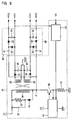
- FIG. 5 A variation of the power source circuit is shown in Figure 5.
- the charge pump circuit 50 is connected to a point B between the inductor 35 and diode 37 in the transmitter power source 14.
- the charge pump circuit 60 is connected to a point C between the inductor 35 and diode 39 in the transmitter power source 14.
- the transmission voltage ⁇ HV1 output by the transmitter power source 14 is supplied to the ultrasonic transducers for use in transmission of ultrasonic signals, and therefore, removal of noise from the transmission voltage ⁇ HV1 is important.
- a voltage drop circuit or a filter circuit is needed.
- Figure 6 shows an exemplary circuit for use in the noise removal for the transmitter power source 14.
- Figure 6(a) is a circuit configuration in which a voltage drop circuit is employed for the noise removing circuit.
- the voltage drop circuit 70 is made from a transistor 71 and a feedback circuit 72.
- the feedback circuit 72 conducts switching control of the transistor 71 with reference to a voltage V4, and the value of voltage +HV1 is reduced by a predetermined amount to output a voltage +HV1a.
- a similar voltage drop circuit is connected to the voltage -HV1, and the value of voltage -HV1 is increased by a predetermined amount to output a voltage -HV1a.
- the transmission/reception beamformer 17 By supplying the voltage +HV1a and -HV1a to the transmission/reception beamformer 17, power source with lower noise than in supplying the voltage ⁇ HV1 is achieved.
- the difference between the voltages +HV1 and +HV1a is of the order of 3 V.
- Figure 6(b) is a circuit configuration in which a filter circuit is employed for the noise removing circuit.
- the filter circuit 75 is made from an inductor 76 and a capacitor 77.
- the filter circuit 75 outputs a voltage +HV1b obtained by removing noise of predetermined frequency from the voltage +HV1.
- a similar filter circuit is connected to the voltage -HV1, and a voltage -HV1b obtained by removing noise of predetermined frequency from the voltage - HV1 is output.
- the charge pump circuits are connected to the transmitter power source for the transmission/reception beamformer 17, and outputs of the charge pump circuits are employed as a bias power source for the analog switch, and therefore, the power source section is reduced in size and power consumption is reduced.
- the power source section can be constructed with a simple configuration and at a low cost.
- a driving circuit for the charge pump may be separately provided, it is possible to use an output of the switching driving circuit in the transmitter power source.
- a circuit design with a high degree of freedom can be realized by using a multi-stage configuration of the charge pump or changing connection points between the charge pumps and transmitter power source.
- cooling means such as forced air cooling is needed if the amount of heat generation from the power source section is large, such cooling means is not needed, and hence, the ultrasonic diagnostic apparatus is further reduced in size.
- analog switch 16 is provided inside the ultrasonic diagnostic apparatus 1 in the present embodiment, the present invention may be applied without limitation on the position of the analog switch; for example, the analog switch may be provided inside the ultrasonic probe.
- a charge pump circuit is employed in the present invention. This is because a capacitor used in the charge pump is smaller and cheaper than a small-size transformer.
- the basic efficacy of the present invention is, however, obtainable by constructing the bias power source from the transmitter power source using the small-size transformer.
Landscapes
- Health & Medical Sciences (AREA)
- Engineering & Computer Science (AREA)
- Life Sciences & Earth Sciences (AREA)
- Physics & Mathematics (AREA)
- Animal Behavior & Ethology (AREA)
- Biomedical Technology (AREA)
- Veterinary Medicine (AREA)
- Public Health (AREA)
- General Health & Medical Sciences (AREA)
- Biophysics (AREA)
- Nuclear Medicine, Radiotherapy & Molecular Imaging (AREA)
- Pathology (AREA)
- Radiology & Medical Imaging (AREA)
- Surgery (AREA)
- Heart & Thoracic Surgery (AREA)
- Medical Informatics (AREA)
- Molecular Biology (AREA)
- Remote Sensing (AREA)
- Computer Networks & Wireless Communication (AREA)
- General Physics & Mathematics (AREA)
- Radar, Positioning & Navigation (AREA)
- Mechanical Engineering (AREA)
- Ultra Sonic Daignosis Equipment (AREA)
- Investigating Or Analyzing Materials By The Use Of Ultrasonic Waves (AREA)
Abstract
Description
Claims (6)
- An ultrasonic diagnostic apparatus for transmitting ultrasonic signals from ultrasonic transducers toward a subject to be examined, and receiving reflected waves of said ultrasonic signals for display, comprising:an analog switch for switching ultrasonic transducers for transmission of said ultrasonic signals and reception of said reflected waves;a transmitter power source for supplying a high voltage to a transmitter circuit for causing said ultrasonic transducers to drive said ultrasonic signals; anda bias power source generating circuit for generating a bias power source for said analog switch from said transmitter power source.
- The ultrasonic diagnostic apparatus of claim 1, wherein said bias power source generating circuit comprises a positive bias power source generating circuit for outputting a voltage value higher than a positive voltage value of said transmitter power source, and a negative bias power source generating circuit for outputting a voltage lower than a negative voltage value of said transmitter power source.
- The ultrasonic diagnostic apparatus of claim 1, wherein a circuit for generating said bias power source from said transmitter power source is a charge pump.
- The ultrasonic diagnostic apparatus of claim 1, wherein said apparatus is a transmission voltage control circuit for variably controlling the voltage value of said transmitter power source.
- The ultrasonic diagnostic apparatus of claim 3 or 4, wherein a driving circuit for said charge pump shares a driving circuit in said transmitter power source.
- The ultrasonic diagnostic apparatus of claim 1, wherein said transmitter power source comprises a stabilizing power source circuit for decreasing and stabilizing the positive voltage value supplied to said transmitter circuit, and a stabilizing power source circuit for increasing and stabilizing the negative voltage value supplied to said transmitter circuit.
Applications Claiming Priority (2)
| Application Number | Priority Date | Filing Date | Title |
|---|---|---|---|
| JP2003029405 | 2003-02-06 | ||
| JP2003029405A JP3964334B2 (en) | 2003-02-06 | 2003-02-06 | Ultrasonic diagnostic equipment |
Publications (3)
| Publication Number | Publication Date |
|---|---|
| EP1445624A2 true EP1445624A2 (en) | 2004-08-11 |
| EP1445624A3 EP1445624A3 (en) | 2005-09-14 |
| EP1445624B1 EP1445624B1 (en) | 2008-08-27 |
Family
ID=32652993
Family Applications (1)
| Application Number | Title | Priority Date | Filing Date |
|---|---|---|---|
| EP04250581A Expired - Lifetime EP1445624B1 (en) | 2003-02-06 | 2004-02-04 | Power source for an ultrasonic diagnostic apparatus |
Country Status (6)
| Country | Link |
|---|---|
| US (1) | US7351204B2 (en) |
| EP (1) | EP1445624B1 (en) |
| JP (1) | JP3964334B2 (en) |
| KR (1) | KR101131677B1 (en) |
| CN (1) | CN1298288C (en) |
| DE (1) | DE602004016067D1 (en) |
Cited By (2)
| Publication number | Priority date | Publication date | Assignee | Title |
|---|---|---|---|---|
| CN102688069A (en) * | 2011-02-04 | 2012-09-26 | Ge医疗系统环球技术有限公司 | Ultrasonic image display apparatus power circuit and ultrasonic image display apparatus |
| WO2017077456A1 (en) * | 2015-11-02 | 2017-05-11 | Koninklijke Philips N.V. | Active distribution of high-voltage power for ultrasound transducers |
Families Citing this family (25)
| Publication number | Priority date | Publication date | Assignee | Title |
|---|---|---|---|---|
| WO2006022106A1 (en) * | 2004-08-24 | 2006-03-02 | Matsushita Electric Industrial Co., Ltd. | Ultrasonic diagnostic apparatus |
| US7967754B2 (en) * | 2004-10-14 | 2011-06-28 | Scimed Life Systems, Inc. | Integrated bias circuitry for ultrasound imaging devices configured to image the interior of a living being |
| JP5348844B2 (en) * | 2004-10-15 | 2013-11-20 | 株式会社日立メディコ | Ultrasonic diagnostic equipment |
| CN1817386B (en) * | 2005-02-08 | 2010-07-21 | 重庆海扶(Hifu)技术有限公司 | Ultrasound diagnosis and treatment device guided by B-ultrasound device |
| JP4822453B2 (en) * | 2005-11-11 | 2011-11-24 | 株式会社日立メディコ | Ultrasonic probe and ultrasonic diagnostic apparatus |
| CN101029929B (en) * | 2006-02-28 | 2011-02-02 | 深圳迈瑞生物医疗电子股份有限公司 | Method for increasing ultrasonic system front-end compatibility and its ultrasonic front-end device |
| JP4886443B2 (en) * | 2006-09-14 | 2012-02-29 | ジーイー・メディカル・システムズ・グローバル・テクノロジー・カンパニー・エルエルシー | Ultrasonic transducer drive circuit and ultrasonic diagnostic apparatus |
| JP2009050372A (en) * | 2007-08-24 | 2009-03-12 | Ge Medical Systems Global Technology Co Llc | Ultrasonic diagnostic apparatus |
| JP2009050367A (en) * | 2007-08-24 | 2009-03-12 | Ge Medical Systems Global Technology Co Llc | Ultrasonic diagnostic apparatus |
| CN101449981B (en) * | 2007-11-30 | 2012-07-11 | 深圳迈瑞生物医疗电子股份有限公司 | Ultrasonic diagnostic device |
| CN101632984B (en) * | 2008-07-24 | 2014-09-17 | Ge医疗系统环球技术有限公司 | Voltage generator circuit and ultrasonic diagnostic equipment |
| KR101089742B1 (en) * | 2009-05-25 | 2011-12-07 | 삼성메디슨 주식회사 | Ultrasonic System for Driving Power Reduction |
| US8790261B2 (en) * | 2009-12-22 | 2014-07-29 | General Electric Company | Manual ultrasound power control to monitor fetal heart rate depending on the size of the patient |
| JP5805961B2 (en) * | 2011-02-24 | 2015-11-10 | ジーイー・メディカル・システムズ・グローバル・テクノロジー・カンパニー・エルエルシー | Power supply circuit for ultrasonic image display device and ultrasonic image display device |
| JP5635540B2 (en) * | 2011-10-26 | 2014-12-03 | ジーイー・メディカル・システムズ・グローバル・テクノロジー・カンパニー・エルエルシー | Reception circuit, ultrasonic probe, and ultrasonic image display device |
| US8933613B2 (en) | 2011-10-28 | 2015-01-13 | General Electric Company | Ultrasonic transducer driving ciruit and ultrasonic image display apparatus |
| US9669427B2 (en) * | 2012-01-24 | 2017-06-06 | Texas Instruments Incorporated | Methods and systems for ultrasound control with bi-directional transistor |
| JP6334937B2 (en) * | 2013-02-07 | 2018-05-30 | キヤノンメディカルシステムズ株式会社 | Ultrasonic diagnostic equipment |
| KR101464257B1 (en) * | 2013-11-12 | 2014-11-21 | 현대모비스 주식회사 | Ultrasonic Wave Parking Assistance Apparatus Using Charge Pumping Circuit for Car and Method Thereof |
| US20150182201A1 (en) * | 2013-12-31 | 2015-07-02 | General Electric Company | Ultrasound probe power supply |
| EP3365115B1 (en) * | 2015-10-21 | 2020-09-30 | Chirp Microsystems, Inc. | Efficient on-chip high-voltage driver circuit for ultrasonic transducer |
| US10667787B2 (en) * | 2016-03-01 | 2020-06-02 | EchoNous, Inc. | Ultrasound system with docking station and dockable ultrasound probe |
| JP6951191B2 (en) * | 2017-10-19 | 2021-10-20 | フクダ電子株式会社 | Voltage supply circuit and ultrasonic diagnostic equipment |
| CN108225389B (en) * | 2017-12-22 | 2020-10-23 | 联创汽车电子有限公司 | Ultrasonic sensor driving device and driving method thereof |
| CN107994802A (en) * | 2017-12-22 | 2018-05-04 | 飞依诺科技(苏州)有限公司 | A kind of supply unit |
Family Cites Families (26)
| Publication number | Priority date | Publication date | Assignee | Title |
|---|---|---|---|---|
| US3581105A (en) * | 1968-09-23 | 1971-05-25 | Bell & Howell Co | Switching apparatus |
| US4092867A (en) | 1977-02-10 | 1978-06-06 | Terrance Matzuk | Ultrasonic scanning apparatus |
| JPS60158840A (en) * | 1984-01-31 | 1985-08-20 | 株式会社東芝 | Ultrasonic diagnostic apparatus |
| US4872145A (en) | 1987-05-04 | 1989-10-03 | Hazeltine Corporation | Noise trap circuit |
| US5081411A (en) * | 1990-12-20 | 1992-01-14 | Honeywell Inc. | AC/DC two-wire control techniques |
| JP3271086B2 (en) * | 1992-09-29 | 2002-04-02 | ソニー株式会社 | Drive circuit for solid-state image sensor |
| US5375051A (en) * | 1992-11-13 | 1994-12-20 | Daiblo Research Corporation | Apparatus using serial data line to turn on a transceiver or other device |
| US5592031A (en) * | 1993-01-28 | 1997-01-07 | Consejo Superior Investigaciones Cientificas | Fast bidirectional analog switching system for HF pulses of high instantaneous power |
| US5509413A (en) | 1993-08-11 | 1996-04-23 | Kabushiki Kaisha Toshiba | Ultrasonic diagnostic apparatus |
| US5610509A (en) | 1994-11-21 | 1997-03-11 | General Electric Company | Method for optimizing power supply voltage to high voltage transmitters |
| US5542425A (en) | 1994-12-20 | 1996-08-06 | Acuson Corporation | Apparatus and method for preventing contact damage in electrical equipment |
| DE4446429C1 (en) | 1994-12-23 | 1996-08-22 | Siemens Ag | Device for treating an object with focused ultrasound waves |
| KR0149220B1 (en) * | 1994-12-27 | 1998-12-01 | 김주용 | Charge pump circuit |
| US5640960A (en) | 1995-04-18 | 1997-06-24 | Imex Medical Systems, Inc. | Hand-held, battery operated, doppler ultrasound medical diagnostic device with cordless probe |
| JPH0993914A (en) * | 1995-09-22 | 1997-04-04 | Toshiba Corp | Multi-output DC / DC converter |
| US6398734B1 (en) | 1997-10-14 | 2002-06-04 | Vascusense, Inc. | Ultrasonic sensors for monitoring the condition of flow through a cardiac valve |
| US6645145B1 (en) * | 1998-11-19 | 2003-11-11 | Siemens Medical Solutions Usa, Inc. | Diagnostic medical ultrasound systems and transducers utilizing micro-mechanical components |
| PT102297A (en) * | 1999-04-28 | 2000-10-31 | Inst Superior Tecnico | INTELLIGENT POWER INTEGRATED CIRCUITS CONFIGURABLE AND SEMICONDUCTOR DEVICES |
| US6310789B1 (en) * | 1999-06-25 | 2001-10-30 | The Procter & Gamble Company | Dynamically-controlled, intrinsically regulated charge pump power converter |
| JP2001190553A (en) | 1999-10-28 | 2001-07-17 | Olympus Optical Co Ltd | Ultrasonograph |
| US6499348B1 (en) | 1999-12-03 | 2002-12-31 | Scimed Life Systems, Inc. | Dynamically configurable ultrasound transducer with integral bias regulation and command and control circuitry |
| JP2001327505A (en) * | 2000-05-22 | 2001-11-27 | Toshiba Corp | Ultrasound diagnostic equipment |
| US6443901B1 (en) * | 2000-06-15 | 2002-09-03 | Koninklijke Philips Electronics N.V. | Capacitive micromachined ultrasonic transducers |
| JP4028692B2 (en) * | 2001-04-05 | 2007-12-26 | ジーイー・メディカル・システムズ・グローバル・テクノロジー・カンパニー・エルエルシー | Ultrasonic diagnostic equipment |
| US6572546B1 (en) * | 2001-07-03 | 2003-06-03 | Acuson Corporation | Two level power supply and method for ultrasound transmission |
| US6795374B2 (en) * | 2001-09-07 | 2004-09-21 | Siemens Medical Solutions Usa, Inc. | Bias control of electrostatic transducers |
-
2003
- 2003-02-06 JP JP2003029405A patent/JP3964334B2/en not_active Expired - Fee Related
-
2004
- 2004-02-04 DE DE602004016067T patent/DE602004016067D1/en not_active Expired - Lifetime
- 2004-02-04 EP EP04250581A patent/EP1445624B1/en not_active Expired - Lifetime
- 2004-02-05 KR KR1020040007391A patent/KR101131677B1/en not_active Expired - Fee Related
- 2004-02-05 US US10/772,879 patent/US7351204B2/en not_active Expired - Fee Related
- 2004-02-06 CN CNB2004100038109A patent/CN1298288C/en not_active Expired - Fee Related
Cited By (4)
| Publication number | Priority date | Publication date | Assignee | Title |
|---|---|---|---|---|
| CN102688069A (en) * | 2011-02-04 | 2012-09-26 | Ge医疗系统环球技术有限公司 | Ultrasonic image display apparatus power circuit and ultrasonic image display apparatus |
| CN102688069B (en) * | 2011-02-04 | 2016-10-05 | Ge医疗系统环球技术有限公司 | Power circuit and ultrasonoscopy display device |
| WO2017077456A1 (en) * | 2015-11-02 | 2017-05-11 | Koninklijke Philips N.V. | Active distribution of high-voltage power for ultrasound transducers |
| US10799220B2 (en) | 2015-11-02 | 2020-10-13 | Koninklijke Philips N.V. | Active distribution of high-voltage power for ultrasound transducers |
Also Published As
| Publication number | Publication date |
|---|---|
| CN1298288C (en) | 2007-02-07 |
| CN1518958A (en) | 2004-08-11 |
| US20040158148A1 (en) | 2004-08-12 |
| US7351204B2 (en) | 2008-04-01 |
| DE602004016067D1 (en) | 2008-10-09 |
| KR20040071632A (en) | 2004-08-12 |
| KR101131677B1 (en) | 2012-03-29 |
| EP1445624A3 (en) | 2005-09-14 |
| JP2004236869A (en) | 2004-08-26 |
| EP1445624B1 (en) | 2008-08-27 |
| JP3964334B2 (en) | 2007-08-22 |
Similar Documents
| Publication | Publication Date | Title |
|---|---|---|
| EP1445624B1 (en) | Power source for an ultrasonic diagnostic apparatus | |
| US8138823B2 (en) | Voltage generating circuit and ultrasonic diagnosing device | |
| US20100041997A1 (en) | Ultrasonic imaging apparatus | |
| JP5384491B2 (en) | Ultrasonic diagnostic equipment | |
| US10527592B2 (en) | Ultrasonic probe, ultrasonic imaging apparatus including the same, and method for controlling the ultrasonic imaging apparatus | |
| EP1932479A1 (en) | Electrostatic capacity type ultrasonic oscillation device and its control method | |
| CN108498116B (en) | Multiple synchronous power supply and ultrasonic system with same | |
| US8925386B2 (en) | Ultrasonic diagnostic apparatus | |
| KR101348769B1 (en) | Ultrasound system for controlling power based on abitrary waveform | |
| CN113907795A (en) | Transceiving system applied to intravascular ultrasonic imaging | |
| JP2018166967A (en) | Medical image diagnostic apparatus | |
| JPH11290321A (en) | Ultrasound diagnostic equipment | |
| WO2010103747A1 (en) | Ultrasonic diagnostic device | |
| JP2006101997A (en) | Ultrasonic probe and ultrasonic diagnostic apparatus | |
| JP5889165B2 (en) | Ultrasonic probe and ultrasonic diagnostic apparatus | |
| US12383227B2 (en) | Ultrasound diagnostic apparatus in which an ultrasound probe is used by switching between a wireless connection mode and a wired connection mode with respect to an apparatus main body and a control method therefor | |
| JP4749448B2 (en) | Ultrasonic imaging device | |
| JP2010194045A (en) | Ultrasonic diagnostic apparatus and transmission unit for ultrasonic diagnostic apparatus | |
| JP5250059B2 (en) | Ultrasonic diagnostic equipment | |
| JP2006015071A (en) | Ultrasonic diagnostic equipment | |
| US20080021320A1 (en) | Inspection device for ultrasonic endoscope apparatus | |
| JPH0630932A (en) | Ultrasonic diagnosing apparatus |
Legal Events
| Date | Code | Title | Description |
|---|---|---|---|
| PUAI | Public reference made under article 153(3) epc to a published international application that has entered the european phase |
Free format text: ORIGINAL CODE: 0009012 |
|
| AK | Designated contracting states |
Kind code of ref document: A2 Designated state(s): AT BE BG CH CY CZ DE DK EE ES FI FR GB GR HU IE IT LI LU MC NL PT RO SE SI SK TR |
|
| AX | Request for extension of the european patent |
Extension state: AL LT LV MK |
|
| PUAL | Search report despatched |
Free format text: ORIGINAL CODE: 0009013 |
|
| AK | Designated contracting states |
Kind code of ref document: A3 Designated state(s): AT BE BG CH CY CZ DE DK EE ES FI FR GB GR HU IE IT LI LU MC NL PT RO SE SI SK TR |
|
| AX | Request for extension of the european patent |
Extension state: AL LT LV MK |
|
| RIC1 | Information provided on ipc code assigned before grant |
Ipc: 7B 06B 1/02 B Ipc: 7G 01S 7/524 B Ipc: 7G 01S 7/52 A Ipc: 7G 01S 7/521 B |
|
| 17P | Request for examination filed |
Effective date: 20060314 |
|
| AKX | Designation fees paid |
Designated state(s): DE FR GB NL |
|
| GRAP | Despatch of communication of intention to grant a patent |
Free format text: ORIGINAL CODE: EPIDOSNIGR1 |
|
| GRAS | Grant fee paid |
Free format text: ORIGINAL CODE: EPIDOSNIGR3 |
|
| GRAA | (expected) grant |
Free format text: ORIGINAL CODE: 0009210 |
|
| AK | Designated contracting states |
Kind code of ref document: B1 Designated state(s): DE FR GB NL |
|
| REG | Reference to a national code |
Ref country code: GB Ref legal event code: FG4D |
|
| REF | Corresponds to: |
Ref document number: 602004016067 Country of ref document: DE Date of ref document: 20081009 Kind code of ref document: P |
|
| PLBE | No opposition filed within time limit |
Free format text: ORIGINAL CODE: 0009261 |
|
| STAA | Information on the status of an ep patent application or granted ep patent |
Free format text: STATUS: NO OPPOSITION FILED WITHIN TIME LIMIT |
|
| 26N | No opposition filed |
Effective date: 20090528 |
|
| GBPC | Gb: european patent ceased through non-payment of renewal fee |
Effective date: 20090204 |
|
| REG | Reference to a national code |
Ref country code: FR Ref legal event code: ST Effective date: 20091030 |
|
| PG25 | Lapsed in a contracting state [announced via postgrant information from national office to epo] |
Ref country code: GB Free format text: LAPSE BECAUSE OF NON-PAYMENT OF DUE FEES Effective date: 20090204 Ref country code: FR Free format text: LAPSE BECAUSE OF NON-PAYMENT OF DUE FEES Effective date: 20090302 |
|
| PGFP | Annual fee paid to national office [announced via postgrant information from national office to epo] |
Ref country code: NL Payment date: 20140226 Year of fee payment: 11 Ref country code: DE Payment date: 20140227 Year of fee payment: 11 |
|
| REG | Reference to a national code |
Ref country code: DE Ref legal event code: R119 Ref document number: 602004016067 Country of ref document: DE |
|
| REG | Reference to a national code |
Ref country code: NL Ref legal event code: V1 Effective date: 20150901 |
|
| PG25 | Lapsed in a contracting state [announced via postgrant information from national office to epo] |
Ref country code: NL Free format text: LAPSE BECAUSE OF NON-PAYMENT OF DUE FEES Effective date: 20150901 |
|
| PG25 | Lapsed in a contracting state [announced via postgrant information from national office to epo] |
Ref country code: DE Free format text: LAPSE BECAUSE OF NON-PAYMENT OF DUE FEES Effective date: 20150901 |