EP1444869B1 - Organic light-emitting device having high luminescent efficiency - Google Patents
Organic light-emitting device having high luminescent efficiency Download PDFInfo
- Publication number
- EP1444869B1 EP1444869B1 EP02781992A EP02781992A EP1444869B1 EP 1444869 B1 EP1444869 B1 EP 1444869B1 EP 02781992 A EP02781992 A EP 02781992A EP 02781992 A EP02781992 A EP 02781992A EP 1444869 B1 EP1444869 B1 EP 1444869B1
- Authority
- EP
- European Patent Office
- Prior art keywords
- layer
- light
- hole
- emitting layer
- organic light
- Prior art date
- Legal status (The legal status is an assumption and is not a legal conclusion. Google has not performed a legal analysis and makes no representation as to the accuracy of the status listed.)
- Expired - Lifetime
Links
Images

Classifications
-
- H—ELECTRICITY
- H05—ELECTRIC TECHNIQUES NOT OTHERWISE PROVIDED FOR
- H05B—ELECTRIC HEATING; ELECTRIC LIGHT SOURCES NOT OTHERWISE PROVIDED FOR; CIRCUIT ARRANGEMENTS FOR ELECTRIC LIGHT SOURCES, IN GENERAL
- H05B33/00—Electroluminescent light sources
- H05B33/12—Light sources with substantially two-dimensional [2D] radiating surfaces
- H05B33/18—Light sources with substantially two-dimensional [2D] radiating surfaces characterised by the nature or concentration of the activator
-
- H—ELECTRICITY
- H10—SEMICONDUCTOR DEVICES; ELECTRIC SOLID-STATE DEVICES NOT OTHERWISE PROVIDED FOR
- H10K—ORGANIC ELECTRIC SOLID-STATE DEVICES
- H10K50/00—Organic light-emitting devices
- H10K50/10—OLEDs or polymer light-emitting diodes [PLED]
- H10K50/14—Carrier transporting layers
-
- H—ELECTRICITY
- H10—SEMICONDUCTOR DEVICES; ELECTRIC SOLID-STATE DEVICES NOT OTHERWISE PROVIDED FOR
- H10K—ORGANIC ELECTRIC SOLID-STATE DEVICES
- H10K50/00—Organic light-emitting devices
-
- H—ELECTRICITY
- H10—SEMICONDUCTOR DEVICES; ELECTRIC SOLID-STATE DEVICES NOT OTHERWISE PROVIDED FOR
- H10K—ORGANIC ELECTRIC SOLID-STATE DEVICES
- H10K50/00—Organic light-emitting devices
- H10K50/10—OLEDs or polymer light-emitting diodes [PLED]
- H10K50/18—Carrier blocking layers
-
- H—ELECTRICITY
- H10—SEMICONDUCTOR DEVICES; ELECTRIC SOLID-STATE DEVICES NOT OTHERWISE PROVIDED FOR
- H10K—ORGANIC ELECTRIC SOLID-STATE DEVICES
- H10K50/00—Organic light-emitting devices
- H10K50/10—OLEDs or polymer light-emitting diodes [PLED]
- H10K50/18—Carrier blocking layers
- H10K50/181—Electron blocking layers
-
- H—ELECTRICITY
- H10—SEMICONDUCTOR DEVICES; ELECTRIC SOLID-STATE DEVICES NOT OTHERWISE PROVIDED FOR
- H10K—ORGANIC ELECTRIC SOLID-STATE DEVICES
- H10K50/00—Organic light-emitting devices
- H10K50/10—OLEDs or polymer light-emitting diodes [PLED]
- H10K50/17—Carrier injection layers
Definitions
- the present invention relates to an organic light-emitting device (OLED) having high luminescent efficiency and, more particularly, to an OLED having high luminescent efficiency and long lifetime in which most holes and electrons are combined in a light-emitting layer of the OLED.
- OLED organic light-emitting device
- an OLED has a transparent anode, a metal cathode and a light-emitting layer including a low molecular or polymeric luminescent organic compound and formed between the anode and the cathode.
- a voltage is applied between the anode and the cathode, light is radiated from the light-emitting layer.
- the OLED has not only a fast response speed but also an excellent brightness and wide viewing angle.
- the OLED has advantages that the OLED operates with a low driving voltage, and full colors in a visible region can be displayed, and it does not need a backlight for light-emitting due to its self-light emitting property.
- the OLED can be manufactured into a thin film and flexible type device, and can be mass-produced by well-known film fabrication techniques.
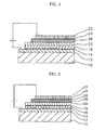
- Fig. 1 shows a cross sectional view of a conventional OLED.
- the OLED includes the first electrode 12 (anode), at least one organic light-emitting layer 20 formed on the first electrode 12, and the second electrode 22 (cathode) formed on the light-emitting layer 20 while facing the first electrode 12.
- the first electrode 12 is made of materials having a high work function, for example, Indium Tin Oxide, polyaniline and Ag
- the second electrode 22 is made of materials having a low work function (generally, less than 4eV), for example, Al, Mg-Ag, Li, and Ca.
- the organic light-emitting layer 20 is composed of an organic luminescent single compound or a conjugated polymer.
- a hole injecting layer 14 and a hole transporting layer 16 are provided between the first electrode 12 and the light-emitting layer 20 to facilitate hole injection and transportation.
- the hole injecting layer 14 is made of materials having an ionization potential higher than that of the anode and lower than that of the light-emitting layer 20
- the hole transporting layer 16 is made of materials having an ionization potential higher than that of the hole injecting layer 14 and lower than that of the light-emitting layer 20.
- an electron injecting layer 24 and an electron transporting layer 26 can be generally provided between the second electrode 22 and the light-emitting layer 20 to facilitate electron injection and transportation.
- the electron injecting layer 24 is made of materials having work function higher than that of the cathode 22 and an electron affinity lower than that of the electron transporting layer 26, and the electron transporting layer 26 is made of materials having an electron affinity higher than that of the electron injecting layer 24 and lower than that of the light-emitting layer 20.
- the hole and the electron are produced at the anode 12 and the cathode 16 by applying a voltage.
- the produced hole and the electron are injected into the light-emitting layer 20 via the hole injecting layer 14, the hole transporting layer 16, the electron injecting layer 24 and the electron transporting layer 26.
- the injected holes and the electrons are recombined in the light-emitting layer 20, which induces light radiation, and the radiated light is displayed through the anode 12 and a substrate 10 made of optically transparent material.
- Amount of holes and electrons injected to the light-emitting layer 20 can be adjusted by modifying the thickness of the hole injecting layer 14, the hole transporting layer 16, the electron injecting layer 24 or the electron transporting layer 26 or by modifying the materials composing the layers.
- the amount of the injected electrons increases. In this case, a part of the injected electrons passes through the light-emitting layer 20, and is extinguished in a layer other than the light-emitting layer 20. Thus, the part of the electron cannot used for light-emitting, which deteriorates the luminescent efficiency of the OLED.
- EP 1 109 234 A2 discloses an organic light emitting device with a multi-layer structure with an emission layer and an electron layer between an anode and a cathode, wherein an intermediate layer comprising a material, having an ionization potential larger than the material used for the emission layer, is provided between the emission layer and electron layer.
- the International Patent application WO 00/16593 also discloses a light emitting device comprising a multi-layer structure including a transparent anode, a hole transporting layer over the anode, an emission layer over the hole transporting layer and a cathode in electrical contact with the electron transporting layer.
- the present invention provides an OLED comprising a first electrode formed on a substrate, at least one organic layer including an organic light-emitting layer, a second electrode formed on the organic layer, a hole inducing layer including a material having an ionization potential higher than that of the organic light-emitting layer and formed between the first electrode and the organic light-emitting layer
- the hole inducing layer is interposed between a hole transporting layer formed on the first electrode and the light-emitting layer.
- the electron blocking layer is interposed between an electron transporting layer formed on the light-emitting layer and the light-emitting layer.
- the hole inducing layer and the electron blocking layer may be formed by being mixed with the hole transporting layer and the electron transporting layer, respectively.
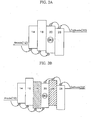
- Fig. 2 is a cross sectional view of an OLED according to an embodiment of the present invention.
- the OLED according to the present invention radiates light by interposing a light emitting organic material between two electrodes, and applying an operation voltage between the electrodes.
- One of the two electrodes must be transparent for transmission of the radiated light.
- the OLED includes an anode 12, a hole injecting layer 14, a hole transporting layer 16, a hole inducing layer 18, a light-emitting layer 20, an electron blocking layer 28, an electron transporting layer 26, an electron injecting layer 24 and a cathode 22, which are successively formed on a substrate 10.
- the hole injecting layer 14 and the electron injecting layer 24 can be optionally formed in accordance with the structure of the OLED.
- the hole inducing layer 18 may be formed by doping or depositing a material having an ionization potential higher than that of the light-emitting layer 20 on the hole transporting layer 16.
- the hole inducing layer 18 may be formed in the hole transporting layer 16 in a mixed form by mixing the material for producing the hole inducing layer 18 with the material for producing the hole transporting layer 16 and then depositing them.
- the hole inducing layer's practical thickness can be 0 to 500 ⁇ , preferably 1 to 100 ⁇ .
- the electron blocking layer 28 may be formed by doping or depositing a material having an electron affinity higher than that of the light-emitting layer 20 on the light-emitting layer 20.
- the electron blocking layer 28 may be formed in the electron transporting layer 26 in a mixed form by mixing the material for producing the electron blocking layer 18 with the material for producing the electron transporting layer 26 and then depositing them.
- the electron blocking layer's practical thickness can be 0 to 500 ⁇ , preferably 1 to 100 ⁇ .
- the hole inducing layer 18 is formed with a material having an ionization potential higher than that of the light-emitting layer 20, that is, with a material having a HOMO energy level lower than that of the light-emitting layer 20.
- the electrons in the light-emitting layer 20 can be inductively injected to the hole inducing layer 18.
- the electron blocking layer 28 is formed with a material having an electron affinity higher than that of the light-emitting layer 20, that is, with a material having a LUMO energy level higher than that of the light-emitting layer 20.
- the amount of the electrons injected into the light-emitting layer 20 can be controlled by the electron blocking layer 28. Therefore, the amount of the electrons and amount of the holes injected to the light-emitting layer 20 can be balanced, and the possibility for recombination of the electrons and the holes in the light-emitting layer 20 increases, and the luminescent efficiency of the OLED increases.
- the OLED of Fig. 2 includes both the hole inducing layer 18 and the electron blocking layer 28, the OLED according to the present invention can include one of the two layers..
- FIG. 3a and 3b The energy band diagrams of OLEDs according to a conventional art and an embodiment of the present invention are shown in Figs. 3a and 3b , respectively.
- the reference numeral depicted in an energy band in Figs. 3a and 3b indicates that the energy band is the energy band of the layer in Fig. 2 to which same reference numeral are designated. As shown in Fig.
- the ionization potentials of the anode 12, the hole injecting layer 14, the hole transporting layer 16, and the light-emitting layer 20 of the conventional OLED gradually increases to naturally induce the hole into the light-emitting layer 20, and the electron affinities of the cathode 14, the electron injecting layer 24, the electron transporting layer 26, and the light-emitting layer 20 of the conventional OLED gradually increases to naturally induce the electron into the light-emitting layer 20.
- the electron blocking layer 28 having the electron affinity higher than that of the light-emitting layer 20 is formed between the electron transporting layer 26 and the light-emitting layer 20, to control the amount of the electrons injected to the light-emitting layer 20.
- the hole inducing layer 18 having the ionization potential higher than that of the light-emitting layer 20 is provided between the hole transporting layer 16 and the light-emitting layer 20, to increase the hole density of the light-emitting layer 20.
- the anode 12 can be made of materials having a high work function, for example, Indium Tin Oxide(ITO), polyaniline and Ag, and the cathode 22 can be made of materials having a low work function, for example, Al, Mg-Ag, Li, and Ca.
- the organic light-emitting layer 20 can be made of various conventional organic compounds under the condition that the organic compounds satisfy the above-described energy relationship with the materials for producing the hole inducing layer 18 and/or the electron blocking layer 28.
- Examples of the organic compounds for producing the organic light-emitting layer 20 include tris(8-quinolinolate)aluminum (Alq 3 ), 10-benzo[h]quinolinol-beryllium complex (BeBq 2 ) or tris(4-methyl-8-quinolinolate)aluminum (Almq), which emits green light (550 nm).
- blue (460nm) luminescent single compound examples include a metal complex such as Bis[2-(2-benzoxazolyl)phenolato]Zinc(II) (ZnPBO) or Bis(2-methyl-8-quinolinolato)(para-phenyl-phenolato)aluminum (Balq) or an organic compound such as strylarylene derivatives, 4,4'-bis(2,2'-biphenylvinyl)-1,1'-biphenyl (DPVBi), oxadiazole derivatives or bisstrylanthracene-based derivatives such as 4,4'-Bis((2-carbazole)vinylene)biphenyl (BczVBi).
- a metal complex such as Bis[2-(2-benzoxazolyl)phenolato]Zinc(II) (ZnPBO) or Bis(2-methyl-8-quinolinolato)(para-phenyl-phenolato)aluminum (Balq
- red (590nm) luminescent organic compound examples include 4-(dicyanomethylene)-2-methyl-6-(p-dimethylaminostyryl)-4H-pyran (DCM) or DCM-based 4-dicyanomethylene-6-cp-julolidinostyryl-2-tert-butyl-4H-pyran (DCJTB).
- DCM 4-(dicyanomethylene)-2-methyl-6-(p-dimethylaminostyryl)-4H-pyran
- DCJTB DCM-based 4-dicyanomethylene-6-cp-julolidinostyryl-2-tert-butyl-4H-pyran
- various other organic compounds or conjugated oligomers or polymers can be used to form the light-emitting layer 20.
- a host material having good electron/hole mobility and the luminescent efficiency and a dopant having various colors can be mixed to form the light-emitting layer 20, which generally called as a guest-host doping system.
- Examples of materials to form the hole injecting layer 14 and the hole transporting layer includes porphyrinic compound such as copper phthalocyanine (CuPc, See United States Patent No. 4,356,429 ), tri(phenyldiamine) derivatives such as N,N'-diphenyl-N,N'bis(3-methylphenyl)-[1,1'-biphenyl]-4,4'-diamine (TPD), 4,4',4"-tris[3-methylphenyl(phenyl)amino]triphenylamine (m-MTDATA), N,N'-diphenyl-N,N'-bis(1-naphthylphenyl)-1,1'-biphenyl-4,4'-diamine ( ⁇ -NPD), N,N,N'N'-tetrakis(m-methylphenyl)-1,3-diaminobenzene (PDA), 1,1-bis[N,N-di(p-toly
- Examples of materials to form the electron injecting layer 24 and the electron transporting layer 26 include LiF, 1,2,4-triazole (TAZ), quinoline derivatives and Alq 3 .
- the materials to form the hole inducing layer 18 or the electron blocking layer 28 can include the materials to form the hole injecting layer 14, the hole transporting layer 16, the electron injecting layer 24 and the electron transporting layer 26 under the condition that the materials for producing the hole inducing layer 18 and/or the electron blocking layer 28 satisfy the above-described energy relationship with the material for producing the light-emitting layer 20.
- the hole inducing layer 18 and/or the electron blocking layer 28 can be made of one or more materials, if necessary to satisfy the above-described energy relationship.
- Layers including the hole inducing layer 18 and the electron blocking layer 28 can be prepared by various conventional methods such as a spin-coating method, a thermal evaporation, a spin-casting method, a sputtering method, an electron-beam evaporation, and a chemical vapor deposition (CVD). Alternatively, two or more materials for producing the layers can be co-deposited by the above-mentioned methods.
- the anode 12 and the cathode 22 can be prepared by a conventional method such as a sputtering method, an ion plating method, a thermal or electron-beam evaporation, or a chemical vapor deposition.
- the thickness of the organic layers are not specifically restricted and can be determined according to the operation condition and the structure of the desired OLED. However, it is preferred that the thickness of each layer is within the range of from 5 nm to 500nm.
- An Indium Tin oxide (ITO) coated glass substrate was ultrasonically washed and then washed with deionized water. The grease on the washed substrate was removed with gas phase toluene, and dried.
- a hole injection layer of thickness of 400 ⁇ was formed by vacuum depositing m-MTDATA on the ITO layer, and a hole transporting layer of thickness of 300 ⁇ was formed by vacuum depositing ⁇ -NPD on the hole injection layer. Then, the mixture of ⁇ -NPD and TAZ was vacuum deposited on the hole transporting layer to form a hole inducing layer of the thickness of about 200 ⁇ .
- the weight ratio of ⁇ -NPD:TAZ can be 1:0.5-1.5, and the ratio was 1:1 in this example.
- Alq3 was vacuum deposited to a thickness of 600 ⁇ to form the organic light-emitting layer.
- TAZ(3-(4-Biphenyl)-4-phenyl-5-tert-butylphenyl)-1,2,4-triazole) was vacuum deposited to a thickness of 380 ⁇ to form an electron transporting layer on the organic light-emitting layer, and LiF of thickness of 7 ⁇ and Ag of thickness of 2000 ⁇ were subsequently deposited on the electron transporting layer to form an electron injection layer and a cathode.
- an OLED was manufactured according to the method described in the above Example.
- the material having the ionization potential higher than that of the light-emitting layer 20 is incorporated between the anode 12 and the light-emitting layer 20, which induces the hole generation and increases the hole density in the light-emitting layer 20.
- the material having the electron affinity higher than that of the light-emitting layer 20 is incorporated between the cathode 22 and the light-emitting layer 20, which controls or decreases the amount of the injected electrons, and minimizes the number of electrons extinguished in a layer other than the light-emitting layer 20. Therefore, the possibility for recombination of the electrons and the holes in the light-emitting layer 20 increases, and the luminescent efficiency and the life time of the OLED increases.
Landscapes
- Physics & Mathematics (AREA)
- Optics & Photonics (AREA)
- Electroluminescent Light Sources (AREA)
- Led Devices (AREA)
- Luminescent Compositions (AREA)
Abstract
Description
- The present invention relates to an organic light-emitting device (OLED) having high luminescent efficiency and, more particularly, to an OLED having high luminescent efficiency and long lifetime in which most holes and electrons are combined in a light-emitting layer of the OLED.
- Generally, an OLED has a transparent anode, a metal cathode and a light-emitting layer including a low molecular or polymeric luminescent organic compound and formed between the anode and the cathode. When a voltage is applied between the anode and the cathode, light is radiated from the light-emitting layer. The OLED has not only a fast response speed but also an excellent brightness and wide viewing angle. Also, the OLED has advantages that the OLED operates with a low driving voltage, and full colors in a visible region can be displayed, and it does not need a backlight for light-emitting due to its self-light emitting property. In addition, the OLED can be manufactured into a thin film and flexible type device, and can be mass-produced by well-known film fabrication techniques.
-
Fig. 1 shows a cross sectional view of a conventional OLED. As shown inFig.1 , the OLED includes the first electrode 12 (anode), at least one organic light-emittinglayer 20 formed on thefirst electrode 12, and the second electrode 22 (cathode) formed on the light-emittinglayer 20 while facing thefirst electrode 12. Conventionally, thefirst electrode 12 is made of materials having a high work function, for example, Indium Tin Oxide, polyaniline and Ag, and thesecond electrode 22 is made of materials having a low work function (generally, less than 4eV), for example, Al, Mg-Ag, Li, and Ca. The organic light-emittinglayer 20 is composed of an organic luminescent single compound or a conjugated polymer. In addition, a hole injectinglayer 14 and ahole transporting layer 16 are provided between thefirst electrode 12 and the light-emittinglayer 20 to facilitate hole injection and transportation. The hole injectinglayer 14 is made of materials having an ionization potential higher than that of the anode and lower than that of the light-emittinglayer 20, and thehole transporting layer 16 is made of materials having an ionization potential higher than that of the hole injectinglayer 14 and lower than that of the light-emittinglayer 20. Also, an electron injectinglayer 24 and anelectron transporting layer 26 can be generally provided between thesecond electrode 22 and the light-emittinglayer 20 to facilitate electron injection and transportation. The electron injectinglayer 24 is made of materials having work function higher than that of thecathode 22 and an electron affinity lower than that of theelectron transporting layer 26, and theelectron transporting layer 26 is made of materials having an electron affinity higher than that of the electron injectinglayer 24 and lower than that of the light-emitting layer 20. - In operation, the hole and the electron are produced at the
anode 12 and thecathode 16 by applying a voltage. The produced hole and the electron are injected into the light-emittinglayer 20 via the hole injectinglayer 14, thehole transporting layer 16, the electron injectinglayer 24 and theelectron transporting layer 26. The injected holes and the electrons are recombined in the light-emittinglayer 20, which induces light radiation, and the radiated light is displayed through theanode 12 and asubstrate 10 made of optically transparent material. - Amount of holes and electrons injected to the light-emitting
layer 20 can be adjusted by modifying the thickness of the hole injectinglayer 14, thehole transporting layer 16, the electron injectinglayer 24 or theelectron transporting layer 26 or by modifying the materials composing the layers. However, it is generally difficult to precisely control the thickness of each layer in a large-size OLED. In addition, as the voltage applied between theanode 12 and thecathode 22 increases, the amount of the injected electrons increases. In this case, a part of the injected electrons passes through the light-emittinglayer 20, and is extinguished in a layer other than the light-emittinglayer 20. Thus, the part of the electron cannot used for light-emitting, which deteriorates the luminescent efficiency of the OLED. - To obtain a favorable colour emission with high efficiency European Patent Application (
EP 1 109 234 A2 - The International Patent application
WO 00/16593 - It is an object of the present invention to provide an OLED having high luminescent efficiency in which most electrons and holes are combined within a light-emitting layer of the OLED.
- It is another object of the present invention to improve the luminescent efficiency of an OLED, thereby to increase the life-time of the OLED.
- To accomplish these objects, the present invention provides an OLED comprising a first electrode formed on a substrate, at least one organic layer including an organic light-emitting layer, a second electrode formed on the organic layer, a hole inducing layer including a material having an ionization potential higher than that of the organic light-emitting layer and formed between the first electrode and the organic light-emitting layer
- The hole inducing layer is interposed between a hole transporting layer formed on the first electrode and the light-emitting layer. Preferably the electron blocking layer is interposed between an electron transporting layer formed on the light-emitting layer and the light-emitting layer. Alternatively, the hole inducing layer and the electron blocking layer may be formed by being mixed with the hole transporting layer and the electron transporting layer, respectively.
- A more complete appreciation of the invention, and many of the attendant advantages thereof, will be readily apparent by reference to the following detailed description when considered in conjunction with the accompanying drawings in which like reference numerals indicate the same or the similar components, wherein:
-
Fig. 1 is a cross sectional view of a conventional OLED; -
Fig. 2 is a cross sectional view of an OLED according to an embodiment of the present invention; -
Figs. 3a and 3b are energy band diagrams of OLEDs according to a conventional art and an embodiment of the present invention, respectively; -
Figs. 4a and 4b are graphs showing the relationship of an applied voltage vs. a current density and a brightness of OLEDs according to a conventional art and an embodiment of the present invention, respectively; and -
Figs. 5a and 5b are graphs showing a relationship of an applied voltage vs. a luminescent efficiency of the OLEDs according to a conventional art and an embodiment of the present invention, respectively. -
Fig. 2 is a cross sectional view of an OLED according to an embodiment of the present invention. As shown inFig.2 , the OLED according to the present invention radiates light by interposing a light emitting organic material between two electrodes, and applying an operation voltage between the electrodes. One of the two electrodes must be transparent for transmission of the radiated light. - As shown in
Fig. 2 , the OLED according to an embodiment of the present invention includes ananode 12, a hole injectinglayer 14, ahole transporting layer 16, ahole inducing layer 18, a light-emitting layer 20, anelectron blocking layer 28, anelectron transporting layer 26, an electron injectinglayer 24 and acathode 22, which are successively formed on asubstrate 10. The hole injectinglayer 14 and the electron injectinglayer 24 can be optionally formed in accordance with the structure of the OLED. - The
hole inducing layer 18 may be formed by doping or depositing a material having an ionization potential higher than that of the light-emittinglayer 20 on thehole transporting layer 16. Alternatively, thehole inducing layer 18 may be formed in thehole transporting layer 16 in a mixed form by mixing the material for producing thehole inducing layer 18 with the material for producing thehole transporting layer 16 and then depositing them. In this case, the hole inducing layer's practical thickness can be 0 to 500Å, preferably 1 to 100Å. - In order to control amount of electrons injected to the light-emitting
layer 20, theelectron blocking layer 28 may be formed by doping or depositing a material having an electron affinity higher than that of the light-emittinglayer 20 on the light-emitting layer 20. Alternatively, theelectron blocking layer 28 may be formed in theelectron transporting layer 26 in a mixed form by mixing the material for producing theelectron blocking layer 18 with the material for producing theelectron transporting layer 26 and then depositing them. In this case, the electron blocking layer's practical thickness can be 0 to 500Å, preferably 1 to 100Å. - In the OLED according to the present invention, the
hole inducing layer 18 is formed with a material having an ionization potential higher than that of the light-emittinglayer 20, that is, with a material having a HOMO energy level lower than that of the light-emittinglayer 20. Thus, the electrons in the light-emittinglayer 20 can be inductively injected to thehole inducing layer 18. Thereby the hole density of the light-emittinglayer 20 increases, and the luminescent efficiency of the OLED increases. Theelectron blocking layer 28 is formed with a material having an electron affinity higher than that of the light-emittinglayer 20, that is, with a material having a LUMO energy level higher than that of the light-emittinglayer 20. Thus, the amount of the electrons injected into the light-emittinglayer 20 can be controlled by theelectron blocking layer 28. Therefore, the amount of the electrons and amount of the holes injected to the light-emittinglayer 20 can be balanced, and the possibility for recombination of the electrons and the holes in the light-emittinglayer 20 increases, and the luminescent efficiency of the OLED increases. Though the OLED ofFig. 2 includes both thehole inducing layer 18 and theelectron blocking layer 28, the OLED according to the present invention can include one of the two layers.. - The energy band diagrams of OLEDs according to a conventional art and an embodiment of the present invention are shown in
Figs. 3a and 3b , respectively. The reference numeral depicted in an energy band inFigs. 3a and 3b indicates that the energy band is the energy band of the layer inFig. 2 to which same reference numeral are designated. As shown inFig. 3A , the ionization potentials of theanode 12, thehole injecting layer 14, thehole transporting layer 16, and the light-emittinglayer 20 of the conventional OLED gradually increases to naturally induce the hole into the light-emittinglayer 20, and the electron affinities of thecathode 14, theelectron injecting layer 24, theelectron transporting layer 26, and the light-emittinglayer 20 of the conventional OLED gradually increases to naturally induce the electron into the light-emittinglayer 20. - In contrast, in the OLED according to an embodiment of the present invention shown in
Fig. 3b , theelectron blocking layer 28 having the electron affinity higher than that of the light-emittinglayer 20 is formed between theelectron transporting layer 26 and the light-emittinglayer 20, to control the amount of the electrons injected to the light-emittinglayer 20. In addition, thehole inducing layer 18 having the ionization potential higher than that of the light-emittinglayer 20 is provided between thehole transporting layer 16 and the light-emittinglayer 20, to increase the hole density of the light-emittinglayer 20. - In the present invention, the
anode 12 can be made of materials having a high work function, for example, Indium Tin Oxide(ITO), polyaniline and Ag, and thecathode 22 can be made of materials having a low work function, for example, Al, Mg-Ag, Li, and Ca. The organic light-emittinglayer 20 can be made of various conventional organic compounds under the condition that the organic compounds satisfy the above-described energy relationship with the materials for producing thehole inducing layer 18 and/or theelectron blocking layer 28. Examples of the organic compounds for producing the organic light-emittinglayer 20 include tris(8-quinolinolate)aluminum (Alq3), 10-benzo[h]quinolinol-beryllium complex (BeBq2) or tris(4-methyl-8-quinolinolate)aluminum (Almq), which emits green light (550 nm). Examples of the blue (460nm) luminescent single compound include a metal complex such as Bis[2-(2-benzoxazolyl)phenolato]Zinc(II) (ZnPBO) or Bis(2-methyl-8-quinolinolato)(para-phenyl-phenolato)aluminum (Balq) or an organic compound such as strylarylene derivatives, 4,4'-bis(2,2'-biphenylvinyl)-1,1'-biphenyl (DPVBi), oxadiazole derivatives or bisstrylanthracene-based derivatives such as 4,4'-Bis((2-carbazole)vinylene)biphenyl (BczVBi). Examples of the red (590nm) luminescent organic compound include 4-(dicyanomethylene)-2-methyl-6-(p-dimethylaminostyryl)-4H-pyran (DCM) or DCM-based 4-dicyanomethylene-6-cp-julolidinostyryl-2-tert-butyl-4H-pyran (DCJTB). Besides these compounds, various other organic compounds or conjugated oligomers or polymers can be used to form the light-emittinglayer 20. In addition, a host material having good electron/hole mobility and the luminescent efficiency and a dopant having various colors can be mixed to form the light-emittinglayer 20, which generally called as a guest-host doping system. - Examples of materials to form the
hole injecting layer 14 and the hole transporting layer includes porphyrinic compound such as copper phthalocyanine (CuPc, See United States Patent No.4,356,429 ), tri(phenyldiamine) derivatives such as N,N'-diphenyl-N,N'bis(3-methylphenyl)-[1,1'-biphenyl]-4,4'-diamine (TPD), 4,4',4"-tris[3-methylphenyl(phenyl)amino]triphenylamine (m-MTDATA), N,N'-diphenyl-N,N'-bis(1-naphthylphenyl)-1,1'-biphenyl-4,4'-diamine (α -NPD), N,N,N'N'-tetrakis(m-methylphenyl)-1,3-diaminobenzene (PDA), 1,1-bis[N,N-di(p-tolyl)aminophenyl]cyclohexane (TPAC), strylamine derivatives and amine derivatives having fused aromatic ring such as N,N'-bis(1-naphthyl)-N,N'-diphenyl-benzidin. Examples of materials to form theelectron injecting layer 24 and theelectron transporting layer 26 include LiF, 1,2,4-triazole (TAZ), quinoline derivatives and Alq3. The materials to form thehole inducing layer 18 or theelectron blocking layer 28 can include the materials to form thehole injecting layer 14, thehole transporting layer 16, theelectron injecting layer 24 and theelectron transporting layer 26 under the condition that the materials for producing thehole inducing layer 18 and/or theelectron blocking layer 28 satisfy the above-described energy relationship with the material for producing the light-emittinglayer 20. Thehole inducing layer 18 and/or theelectron blocking layer 28 can be made of one or more materials, if necessary to satisfy the above-described energy relationship. Layers including thehole inducing layer 18 and theelectron blocking layer 28 can be prepared by various conventional methods such as a spin-coating method, a thermal evaporation, a spin-casting method, a sputtering method, an electron-beam evaporation, and a chemical vapor deposition (CVD). Alternatively, two or more materials for producing the layers can be co-deposited by the above-mentioned methods. Theanode 12 and thecathode 22 can be prepared by a conventional method such as a sputtering method, an ion plating method, a thermal or electron-beam evaporation, or a chemical vapor deposition. The thickness of the organic layers are not specifically restricted and can be determined according to the operation condition and the structure of the desired OLED. However, it is preferred that the thickness of each layer is within the range of from 5 nm to 500nm. - Hereinafter, the present invention will be explained in detail with reference to an example and a comparative example.
- An Indium Tin oxide (ITO) coated glass substrate was ultrasonically washed and then washed with deionized water. The grease on the washed substrate was removed with gas phase toluene, and dried. To produce an OLED, a hole injection layer of thickness of 400Å was formed by vacuum depositing m-MTDATA on the ITO layer, and a hole transporting layer of thickness of 300Å was formed by vacuum depositing α -NPD on the hole injection layer. Then, the mixture of α -NPD and TAZ was vacuum deposited on the hole transporting layer to form a hole inducing layer of the thickness of about 200Å. The weight ratio of α -NPD:TAZ can be 1:0.5-1.5, and the ratio was 1:1 in this example. As the organic luminescent compound, Alq3 was vacuum deposited to a thickness of 600 Å to form the organic light-emitting layer. Then, TAZ(3-(4-Biphenyl)-4-phenyl-5-tert-butylphenyl)-1,2,4-triazole) was vacuum deposited to a thickness of 380Å to form an electron transporting layer on the organic light-emitting layer, and LiF of thickness of 7Å and Ag of thickness of 2000Å were subsequently deposited on the electron transporting layer to form an electron injection layer and a cathode.
- Except for not depositing the mixture of α -NPD and TAZ for forming the hole inducing layer, an OLED was manufactured according to the method described in the above Example.
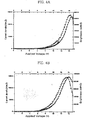
- The relationship of an applied voltage vs. a current density and a brightness of the OLEDs according to the Comparative Example and the Example were measured, and shown in
Figs. 4a and 4b , respectively. InFigs. 4A and 4B , the symbol "□" stands for the brightness and the symbol " ■" stands for the current density. As shown inFigs. 4a and 4b , the brightness of the OLED of the Example (Fig. 4B ) is very high in comparison with that of the OLED of the Comparative Example(Fig. 4A ). The relationship of an applied voltage vs. a luminescent efficiency of the OLEDs according to the Comparative Example and the Example were measured, and shown inFigs. 5a and 5b , respectively. The luminescent efficiency η was calculated by the equation η = π x L/[V x J], wherein L represents a brightness, V represents an applied voltage, and J represents a current density. As shown inFigs. 5a and 5b , the luminescent efficiency of the OLED of the Example (Fig. 5B ) is very high in comparison with that of the OLED of the Comparative Example(Fig. 5A ), especially at low applied voltage. - In the OLED of the present invention, the material having the ionization potential higher than that of the light-emitting
layer 20 is incorporated between theanode 12 and the light-emittinglayer 20, which induces the hole generation and increases the hole density in the light-emittinglayer 20. Also, the material having the electron affinity higher than that of the light-emittinglayer 20 is incorporated between thecathode 22 and the light-emittinglayer 20, which controls or decreases the amount of the injected electrons, and minimizes the number of electrons extinguished in a layer other than the light-emittinglayer 20. Therefore, the possibility for recombination of the electrons and the holes in the light-emittinglayer 20 increases, and the luminescent efficiency and the life time of the OLED increases.
Claims (6)
- An organic light-emitting device comprising:a first electrode formed on a substrate:at least one organic layer including an organic light-emitting layer formed on the first electrode;a second electrode formed on the organic layer; anda hole inducing layer including a material having an ionization potential higher than that of the organic light-emitting layer and formed between the first electrode and the organic light-emitting layer,further comprising a hole transporting layer formed on the first electrode,characterised in that the hole inducing layer is formed between the hole transporting layer and the organic light-emitting layer.
- The organic light-emitting device according to claim 1, wherein the hole inducing layer is formed by being mixed with the hole transporting layer.
- The organic light-emitting device according to claim 1, further comprising an electron transporting layer formed on the light-emitting layer.
- The organic light-emitting device according to claim 1, further comprising a hole injecting layer on the first electrode, and an electron injecting layer under the second electrode.
- The organic light-emitting device according to claim 1, wherein the first electrode is made of ITO, the second electrode is made of Ag, the hole inducing layer includes the mixture of alpha-NPD and TAZ and the organic light-emitting layer is made of Alq3.
- The organic light-emitting device according to claim 5, further comprising a hole injecting layer formed on the first electrode and comprising m-MTDATA, a hole transporting layer formed on the hole injecting layer and comprising alpha-NPD, and wherein the hole inducing layer is formed on the hole transporting layer and made of the mixture of alpha-NPD and TAZ.
Applications Claiming Priority (3)
| Application Number | Priority Date | Filing Date | Title |
|---|---|---|---|
| KR1020010070024A KR100596028B1 (en) | 2001-11-12 | 2001-11-12 | High Efficiency Organic Electroluminescent Devices |
| KR2001070024 | 2001-11-12 | ||
| PCT/KR2002/002021 WO2003043383A1 (en) | 2001-11-12 | 2002-10-30 | Organic light-emitting device having high luminescent efficiency |
Publications (3)
| Publication Number | Publication Date |
|---|---|
| EP1444869A1 EP1444869A1 (en) | 2004-08-11 |
| EP1444869A4 EP1444869A4 (en) | 2008-05-28 |
| EP1444869B1 true EP1444869B1 (en) | 2011-04-13 |
Family
ID=19715895
Family Applications (1)
| Application Number | Title | Priority Date | Filing Date |
|---|---|---|---|
| EP02781992A Expired - Lifetime EP1444869B1 (en) | 2001-11-12 | 2002-10-30 | Organic light-emitting device having high luminescent efficiency |
Country Status (8)
| Country | Link |
|---|---|
| US (1) | US20040245542A1 (en) |
| EP (1) | EP1444869B1 (en) |
| JP (1) | JP2005510025A (en) |
| KR (1) | KR100596028B1 (en) |
| CN (1) | CN1586095A (en) |
| AT (1) | ATE505935T1 (en) |
| DE (1) | DE60239755D1 (en) |
| WO (1) | WO2003043383A1 (en) |
Families Citing this family (34)
| Publication number | Priority date | Publication date | Assignee | Title |
|---|---|---|---|---|
| US20050069727A1 (en) * | 2003-09-30 | 2005-03-31 | Rahul Gupta | Oled emissive polymer layer |
| JPWO2005076668A1 (en) * | 2004-02-06 | 2007-10-18 | 出光興産株式会社 | Organic electroluminescence device |
| US20060017057A1 (en) * | 2004-07-20 | 2006-01-26 | Cumpston Brian H | Device structure to improve OLED reliability |
| US20060115673A1 (en) * | 2004-12-01 | 2006-06-01 | Au Optronics Corporation | Organic light emitting device with improved electrode structure |
| TW200714131A (en) * | 2005-07-29 | 2007-04-01 | Sanyo Electric Co | Organic electroluminescent element and organic electroluminescent display device |
| JP2007035579A (en) * | 2005-07-29 | 2007-02-08 | Sanyo Electric Co Ltd | Organic electroluminescent device and organic electroluminescent display device |
| US8148891B2 (en) * | 2005-10-04 | 2012-04-03 | Universal Display Corporation | Electron impeding layer for high efficiency phosphorescent OLEDs |
| JP4673279B2 (en) * | 2005-12-20 | 2011-04-20 | 三星モバイルディスプレイ株式會社 | Organic light emitting display device and method for manufacturing the same |
| WO2008069153A1 (en) * | 2006-12-04 | 2008-06-12 | Semiconductor Energy Laboratory Co., Ltd. | Light-emitting element, light-emitting device, and electronic device |
| JP5380275B2 (en) * | 2007-02-19 | 2014-01-08 | 大日本印刷株式会社 | Organic electroluminescence device |
| US20080238300A1 (en) * | 2007-04-02 | 2008-10-02 | Sang Tae Park | Organic electroluminescence device and method for fabricating the same |
| JP5530608B2 (en) * | 2007-09-13 | 2014-06-25 | 株式会社半導体エネルギー研究所 | Light emitting element and light emitting device |
| US8115382B2 (en) | 2007-09-20 | 2012-02-14 | Semiconductor Energy Laboratory Co., Ltd. | Light-emitting element, light-emitting device, and electronic device, comprising controlled carrier transport |
| TWI481308B (en) * | 2007-09-27 | 2015-04-11 | Semiconductor Energy Lab | Light-emitting element, light-emitting device, and electronic device |
| JP5540600B2 (en) * | 2008-08-13 | 2014-07-02 | 三菱化学株式会社 | Electronic device, organic electroluminescent element, organic EL display device, and organic EL lighting |
| JP5293120B2 (en) * | 2008-11-28 | 2013-09-18 | 住友化学株式会社 | Organic electroluminescence device and method for producing the same |
| JP2013545293A (en) * | 2010-10-20 | 2013-12-19 | ▲海▼洋王照明科技股▲ふん▼有限公司 | Organic electroluminescent device and manufacturing method thereof |
| KR102017745B1 (en) | 2012-10-12 | 2019-09-04 | 삼성디스플레이 주식회사 | Organic light-emitting diode, method for preparing the same, and organic light-emitting devise including the same |
| CN103730581B (en) * | 2012-10-15 | 2016-05-18 | 乐金显示有限公司 | Organic light emitting apparatus and the organic light-emitting display device that uses it |
| KR102367337B1 (en) | 2014-11-26 | 2022-02-25 | 삼성디스플레이 주식회사 | Organic light emitting diode and display panel having the same |
| CN105244446B (en) | 2015-08-28 | 2018-06-29 | 京东方科技集团股份有限公司 | Organic electroluminescence device and preparation method thereof, display device |
| US10270041B2 (en) * | 2015-08-28 | 2019-04-23 | Semiconductor Energy Laboratory Co., Ltd. | Light-emitting element, light-emitting device, electronic device, and lighting device |
| CN113773298A (en) | 2015-12-17 | 2021-12-10 | 株式会社半导体能源研究所 | Light-emitting element, light-emitting device, electronic equipment, lighting device, lighting system and guidance system |
| US10388900B2 (en) | 2016-07-28 | 2019-08-20 | Semiconductor Energy Laboratory Co., Ltd. | Light-emitting element, light-emitting device, electronic device, and lighting device |
| KR102701648B1 (en) | 2016-12-28 | 2024-09-03 | 가부시키가이샤 한도오따이 에네루기 켄큐쇼 | Organic compound, light-emitting element, light-emitting device, electronic device, display device, and lighting device |
| CN107195791B (en) * | 2017-05-03 | 2019-01-01 | 武汉华星光电技术有限公司 | Organic light-emitting display device |
| US11342524B2 (en) * | 2018-03-30 | 2022-05-24 | Sharp Kabushiki Kaisha | Light emitting element, light emitting device, and apparatus for producing light emitting element |
| CN113498631A (en) * | 2019-02-26 | 2021-10-12 | 夏普株式会社 | Light emitting element and light emitting device |
| JP2020188199A (en) * | 2019-05-16 | 2020-11-19 | 株式会社Joled | Organic el element, organic el display panel, and manufacturing method of organic el element |
| CN110364636B (en) * | 2019-07-22 | 2022-02-22 | 云谷(固安)科技有限公司 | Organic electroluminescent device and display device |
| JP7438509B2 (en) * | 2019-08-02 | 2024-02-27 | 国立大学法人九州大学 | Light emitting device, light emitting method and organic light emitting device |
| US11925046B2 (en) | 2019-08-02 | 2024-03-05 | Kyushu University, National University Corporation | Light-emitting device, light-emitting method, and organic light-emitting element |
| CN115701229A (en) * | 2021-07-30 | 2023-02-07 | 京东方科技集团股份有限公司 | Light emitting diode device, manufacturing method thereof, light emitting substrate and light emitting device |
| CN114551743A (en) * | 2022-02-24 | 2022-05-27 | 京东方科技集团股份有限公司 | Light-emitting device, preparation method thereof, display substrate and display device |
Family Cites Families (25)
| Publication number | Priority date | Publication date | Assignee | Title |
|---|---|---|---|---|
| US4539507A (en) * | 1983-03-25 | 1985-09-03 | Eastman Kodak Company | Organic electroluminescent devices having improved power conversion efficiencies |
| JP3476855B2 (en) * | 1992-01-07 | 2003-12-10 | 株式会社東芝 | Organic EL device |
| JPH08138868A (en) * | 1994-09-16 | 1996-05-31 | Ricoh Co Ltd | Organic thin film EL device |
| US5645948A (en) * | 1996-08-20 | 1997-07-08 | Eastman Kodak Company | Blue organic electroluminescent devices |
| KR100292830B1 (en) * | 1998-09-17 | 2001-07-12 | 김덕중 | Organic light-emitting device having improved luminous efficiency |
| GB9810798D0 (en) * | 1998-05-20 | 1998-07-15 | Sharp Kk | Light emitting devices |
| JPH11354278A (en) * | 1998-06-08 | 1999-12-24 | Fuji Photo Film Co Ltd | Organic electroluminescent device material and organic electroluminescent device using the same |
| JP2000012237A (en) * | 1998-06-25 | 2000-01-14 | Nec Corp | Manufacturing method of organic electroluminescent display device |
| JP2000040589A (en) * | 1998-07-22 | 2000-02-08 | Tdk Corp | Organic EL device |
| US6097147A (en) * | 1998-09-14 | 2000-08-01 | The Trustees Of Princeton University | Structure for high efficiency electroluminescent device |
| US6361886B2 (en) * | 1998-12-09 | 2002-03-26 | Eastman Kodak Company | Electroluminescent device with improved hole transport layer |
| JP2000196140A (en) * | 1998-12-28 | 2000-07-14 | Sharp Corp | Organic electroluminescent device and manufacturing method thereof |
| JP3125777B2 (en) * | 1999-01-28 | 2001-01-22 | 日本電気株式会社 | Organic electroluminescence device and panel |
| JP2000235893A (en) * | 1999-02-15 | 2000-08-29 | Idemitsu Kosan Co Ltd | Organic electroluminescence device and method of manufacturing the same |
| JP2000268959A (en) * | 1999-03-12 | 2000-09-29 | Toyota Motor Corp | Method for changing emission color of organic EL element |
| JP4395216B2 (en) * | 1999-05-07 | 2010-01-06 | 矢崎総業株式会社 | Instrument with self-luminous guidelines and self-luminous guidelines |
| JP3885412B2 (en) * | 1999-05-25 | 2007-02-21 | 松下電器産業株式会社 | Organic electroluminescence device |
| US6528940B1 (en) * | 1999-09-28 | 2003-03-04 | Canon Kabushiki Kaisha | Conductive liquid crystal device, and organic electroluminescence device |
| JP2001167886A (en) * | 1999-12-13 | 2001-06-22 | Nec Corp | Organic electroluminescence device |
| JP4068279B2 (en) * | 2000-02-23 | 2008-03-26 | パイオニア株式会社 | Organic electroluminescence device |
| TWI226205B (en) * | 2000-03-27 | 2005-01-01 | Semiconductor Energy Lab | Self-light emitting device and method of manufacturing the same |
| JP2002367786A (en) * | 2001-06-08 | 2002-12-20 | Toray Ind Inc | Luminous element |
| WO2002104080A1 (en) * | 2001-06-15 | 2002-12-27 | Canon Kabushiki Kaisha | Organic electroluminescnece device |
| US6727644B2 (en) * | 2001-08-06 | 2004-04-27 | Eastman Kodak Company | Organic light-emitting device having a color-neutral dopant in an emission layer and in a hole and/or electron transport sublayer |
| US6835469B2 (en) * | 2001-10-17 | 2004-12-28 | The University Of Southern California | Phosphorescent compounds and devices comprising the same |
-
2001
- 2001-11-12 KR KR1020010070024A patent/KR100596028B1/en not_active Expired - Fee Related
-
2002
- 2002-10-30 WO PCT/KR2002/002021 patent/WO2003043383A1/en not_active Ceased
- 2002-10-30 AT AT02781992T patent/ATE505935T1/en not_active IP Right Cessation
- 2002-10-30 CN CNA028222954A patent/CN1586095A/en active Pending
- 2002-10-30 DE DE60239755T patent/DE60239755D1/en not_active Expired - Lifetime
- 2002-10-30 EP EP02781992A patent/EP1444869B1/en not_active Expired - Lifetime
- 2002-10-30 JP JP2003545077A patent/JP2005510025A/en active Pending
-
2004
- 2004-04-22 US US10/830,256 patent/US20040245542A1/en not_active Abandoned
Also Published As
| Publication number | Publication date |
|---|---|
| CN1586095A (en) | 2005-02-23 |
| WO2003043383A1 (en) | 2003-05-22 |
| JP2005510025A (en) | 2005-04-14 |
| DE60239755D1 (en) | 2011-05-26 |
| EP1444869A1 (en) | 2004-08-11 |
| EP1444869A4 (en) | 2008-05-28 |
| ATE505935T1 (en) | 2011-04-15 |
| KR100596028B1 (en) | 2006-07-03 |
| US20040245542A1 (en) | 2004-12-09 |
| KR20030039100A (en) | 2003-05-17 |
Similar Documents
| Publication | Publication Date | Title |
|---|---|---|
| US20040245542A1 (en) | Organic light-emitting device having high luminescent efficiency | |
| KR100329571B1 (en) | Organic electroluminescent device | |
| KR100922759B1 (en) | Organic light emitting device | |
| KR100922760B1 (en) | Organic light emitting device | |
| US6150043A (en) | OLEDs containing thermally stable glassy organic hole transporting materials | |
| US6392250B1 (en) | Organic light emitting devices having improved performance | |
| CN100372144C (en) | Organic Electroluminescent Devices | |
| US6627333B2 (en) | White organic light-emitting devices with improved efficiency | |
| US6720092B2 (en) | White organic light-emitting devices using rubrene layer | |
| US8557398B2 (en) | Organic light emitting device | |
| US6806491B2 (en) | Organic light-emitting devices | |
| WO2001039234A2 (en) | Organic light emitting diode having a blue phosphorescent molecule as an emitter | |
| KR20090072447A (en) | Organic light emitting device | |
| KR20090050369A (en) | Organic light emitting device | |
| EP1296386A2 (en) | Sputtered cathode having a heavy alkaline metal halide in an organic light-emitting device structure | |
| KR100894066B1 (en) | Organic light emitting device | |
| KR100879476B1 (en) | Organic light emitting device | |
| WO2002102117A1 (en) | Three-terminal organic electro-luminescent device | |
| JPH10335066A (en) | Organic electroluminescent device and flat panel display using the same | |
| JPH1060427A (en) | Organic el element produced by using coumarin derivative | |
| KR100898075B1 (en) | Organic light emitting device | |
| JP3763325B2 (en) | Organic electroluminescence device | |
| JPH10223372A (en) | Organic electroluminescent device and flat panel display using the same | |
| KR20040100523A (en) | White organic light emitting device using three emissive layer | |
| KR100594775B1 (en) | White organic light emitting device |
Legal Events
| Date | Code | Title | Description |
|---|---|---|---|
| PUAI | Public reference made under article 153(3) epc to a published international application that has entered the european phase |
Free format text: ORIGINAL CODE: 0009012 |
|
| 17P | Request for examination filed |
Effective date: 20040507 |
|
| AK | Designated contracting states |
Kind code of ref document: A1 Designated state(s): AT BE BG CH CY CZ DE DK EE ES FI FR GB GR IE IT LI LU MC NL PT SE SK TR |
|
| AX | Request for extension of the european patent |
Extension state: AL LT LV MK RO SI |
|
| A4 | Supplementary search report drawn up and despatched |
Effective date: 20080428 |
|
| 17Q | First examination report despatched |
Effective date: 20090126 |
|
| GRAP | Despatch of communication of intention to grant a patent |
Free format text: ORIGINAL CODE: EPIDOSNIGR1 |
|
| RIN1 | Information on inventor provided before grant (corrected) |
Inventor name: KIM, HAE-WON Inventor name: IM,WOO-BIN, |
|
| GRAS | Grant fee paid |
Free format text: ORIGINAL CODE: EPIDOSNIGR3 |
|
| GRAA | (expected) grant |
Free format text: ORIGINAL CODE: 0009210 |
|
| AK | Designated contracting states |
Kind code of ref document: B1 Designated state(s): AT BE BG CH CY CZ DE DK EE ES FI FR GB GR IE IT LI LU MC NL PT SE SK TR |
|
| REG | Reference to a national code |
Ref country code: GB Ref legal event code: FG4D |
|
| REG | Reference to a national code |
Ref country code: CH Ref legal event code: EP |
|
| REG | Reference to a national code |
Ref country code: IE Ref legal event code: FG4D |
|
| REF | Corresponds to: |
Ref document number: 60239755 Country of ref document: DE Date of ref document: 20110526 Kind code of ref document: P |
|
| REG | Reference to a national code |
Ref country code: DE Ref legal event code: R096 Ref document number: 60239755 Country of ref document: DE Effective date: 20110526 |
|
| REG | Reference to a national code |
Ref country code: NL Ref legal event code: VDEP Effective date: 20110413 |
|
| PG25 | Lapsed in a contracting state [announced via postgrant information from national office to epo] |
Ref country code: SE Free format text: LAPSE BECAUSE OF FAILURE TO SUBMIT A TRANSLATION OF THE DESCRIPTION OR TO PAY THE FEE WITHIN THE PRESCRIBED TIME-LIMIT Effective date: 20110413 Ref country code: PT Free format text: LAPSE BECAUSE OF FAILURE TO SUBMIT A TRANSLATION OF THE DESCRIPTION OR TO PAY THE FEE WITHIN THE PRESCRIBED TIME-LIMIT Effective date: 20110816 |
|
| PG25 | Lapsed in a contracting state [announced via postgrant information from national office to epo] |
Ref country code: BE Free format text: LAPSE BECAUSE OF FAILURE TO SUBMIT A TRANSLATION OF THE DESCRIPTION OR TO PAY THE FEE WITHIN THE PRESCRIBED TIME-LIMIT Effective date: 20110413 Ref country code: CY Free format text: LAPSE BECAUSE OF FAILURE TO SUBMIT A TRANSLATION OF THE DESCRIPTION OR TO PAY THE FEE WITHIN THE PRESCRIBED TIME-LIMIT Effective date: 20110413 Ref country code: FI Free format text: LAPSE BECAUSE OF FAILURE TO SUBMIT A TRANSLATION OF THE DESCRIPTION OR TO PAY THE FEE WITHIN THE PRESCRIBED TIME-LIMIT Effective date: 20110413 Ref country code: AT Free format text: LAPSE BECAUSE OF FAILURE TO SUBMIT A TRANSLATION OF THE DESCRIPTION OR TO PAY THE FEE WITHIN THE PRESCRIBED TIME-LIMIT Effective date: 20110413 Ref country code: GR Free format text: LAPSE BECAUSE OF FAILURE TO SUBMIT A TRANSLATION OF THE DESCRIPTION OR TO PAY THE FEE WITHIN THE PRESCRIBED TIME-LIMIT Effective date: 20110714 Ref country code: ES Free format text: LAPSE BECAUSE OF FAILURE TO SUBMIT A TRANSLATION OF THE DESCRIPTION OR TO PAY THE FEE WITHIN THE PRESCRIBED TIME-LIMIT Effective date: 20110724 |
|
| PG25 | Lapsed in a contracting state [announced via postgrant information from national office to epo] |
Ref country code: NL Free format text: LAPSE BECAUSE OF FAILURE TO SUBMIT A TRANSLATION OF THE DESCRIPTION OR TO PAY THE FEE WITHIN THE PRESCRIBED TIME-LIMIT Effective date: 20110413 |
|
| PG25 | Lapsed in a contracting state [announced via postgrant information from national office to epo] |
Ref country code: CZ Free format text: LAPSE BECAUSE OF FAILURE TO SUBMIT A TRANSLATION OF THE DESCRIPTION OR TO PAY THE FEE WITHIN THE PRESCRIBED TIME-LIMIT Effective date: 20110413 Ref country code: EE Free format text: LAPSE BECAUSE OF FAILURE TO SUBMIT A TRANSLATION OF THE DESCRIPTION OR TO PAY THE FEE WITHIN THE PRESCRIBED TIME-LIMIT Effective date: 20110413 |
|
| PLBE | No opposition filed within time limit |
Free format text: ORIGINAL CODE: 0009261 |
|
| STAA | Information on the status of an ep patent application or granted ep patent |
Free format text: STATUS: NO OPPOSITION FILED WITHIN TIME LIMIT |
|
| PG25 | Lapsed in a contracting state [announced via postgrant information from national office to epo] |
Ref country code: DK Free format text: LAPSE BECAUSE OF FAILURE TO SUBMIT A TRANSLATION OF THE DESCRIPTION OR TO PAY THE FEE WITHIN THE PRESCRIBED TIME-LIMIT Effective date: 20110413 Ref country code: SK Free format text: LAPSE BECAUSE OF FAILURE TO SUBMIT A TRANSLATION OF THE DESCRIPTION OR TO PAY THE FEE WITHIN THE PRESCRIBED TIME-LIMIT Effective date: 20110413 |
|
| 26N | No opposition filed |
Effective date: 20120116 |
|
| REG | Reference to a national code |
Ref country code: DE Ref legal event code: R097 Ref document number: 60239755 Country of ref document: DE Effective date: 20120116 |
|
| PG25 | Lapsed in a contracting state [announced via postgrant information from national office to epo] |
Ref country code: MC Free format text: LAPSE BECAUSE OF NON-PAYMENT OF DUE FEES Effective date: 20111031 Ref country code: IT Free format text: LAPSE BECAUSE OF FAILURE TO SUBMIT A TRANSLATION OF THE DESCRIPTION OR TO PAY THE FEE WITHIN THE PRESCRIBED TIME-LIMIT Effective date: 20110413 |
|
| REG | Reference to a national code |
Ref country code: CH Ref legal event code: PL |
|
| PG25 | Lapsed in a contracting state [announced via postgrant information from national office to epo] |
Ref country code: LI Free format text: LAPSE BECAUSE OF NON-PAYMENT OF DUE FEES Effective date: 20111031 Ref country code: CH Free format text: LAPSE BECAUSE OF NON-PAYMENT OF DUE FEES Effective date: 20111031 |
|
| REG | Reference to a national code |
Ref country code: IE Ref legal event code: MM4A |
|
| PG25 | Lapsed in a contracting state [announced via postgrant information from national office to epo] |
Ref country code: IE Free format text: LAPSE BECAUSE OF NON-PAYMENT OF DUE FEES Effective date: 20111030 |
|
| PG25 | Lapsed in a contracting state [announced via postgrant information from national office to epo] |
Ref country code: LU Free format text: LAPSE BECAUSE OF NON-PAYMENT OF DUE FEES Effective date: 20111030 |
|
| PG25 | Lapsed in a contracting state [announced via postgrant information from national office to epo] |
Ref country code: BG Free format text: LAPSE BECAUSE OF FAILURE TO SUBMIT A TRANSLATION OF THE DESCRIPTION OR TO PAY THE FEE WITHIN THE PRESCRIBED TIME-LIMIT Effective date: 20110713 |
|
| PG25 | Lapsed in a contracting state [announced via postgrant information from national office to epo] |
Ref country code: TR Free format text: LAPSE BECAUSE OF FAILURE TO SUBMIT A TRANSLATION OF THE DESCRIPTION OR TO PAY THE FEE WITHIN THE PRESCRIBED TIME-LIMIT Effective date: 20110413 |
|
| REG | Reference to a national code |
Ref country code: FR Ref legal event code: PLFP Year of fee payment: 15 |
|
| REG | Reference to a national code |
Ref country code: FR Ref legal event code: PLFP Year of fee payment: 16 |
|
| REG | Reference to a national code |
Ref country code: FR Ref legal event code: PLFP Year of fee payment: 17 |
|
| PGFP | Annual fee paid to national office [announced via postgrant information from national office to epo] |
Ref country code: GB Payment date: 20200910 Year of fee payment: 19 Ref country code: FR Payment date: 20200910 Year of fee payment: 19 |
|
| PGFP | Annual fee paid to national office [announced via postgrant information from national office to epo] |
Ref country code: DE Payment date: 20200908 Year of fee payment: 19 |
|
| REG | Reference to a national code |
Ref country code: DE Ref legal event code: R119 Ref document number: 60239755 Country of ref document: DE |
|
| GBPC | Gb: european patent ceased through non-payment of renewal fee |
Effective date: 20211030 |
|
| PG25 | Lapsed in a contracting state [announced via postgrant information from national office to epo] |
Ref country code: GB Free format text: LAPSE BECAUSE OF NON-PAYMENT OF DUE FEES Effective date: 20211030 Ref country code: DE Free format text: LAPSE BECAUSE OF NON-PAYMENT OF DUE FEES Effective date: 20220503 |
|
| PG25 | Lapsed in a contracting state [announced via postgrant information from national office to epo] |
Ref country code: FR Free format text: LAPSE BECAUSE OF NON-PAYMENT OF DUE FEES Effective date: 20211031 |