EP1443670A2 - Digital baseband modulation apparatus and demodulation apparatus - Google Patents
Digital baseband modulation apparatus and demodulation apparatus Download PDFInfo
- Publication number
- EP1443670A2 EP1443670A2 EP04000697A EP04000697A EP1443670A2 EP 1443670 A2 EP1443670 A2 EP 1443670A2 EP 04000697 A EP04000697 A EP 04000697A EP 04000697 A EP04000697 A EP 04000697A EP 1443670 A2 EP1443670 A2 EP 1443670A2
- Authority
- EP
- European Patent Office
- Prior art keywords
- signal
- component
- output
- axis
- amplitude
- Prior art date
- Legal status (The legal status is an assumption and is not a legal conclusion. Google has not performed a legal analysis and makes no representation as to the accuracy of the status listed.)
- Granted
Links
Images








Classifications
-
- H—ELECTRICITY
- H04—ELECTRIC COMMUNICATION TECHNIQUE
- H04B—TRANSMISSION
- H04B1/00—Details of transmission systems, not covered by a single one of groups H04B3/00 - H04B13/00; Details of transmission systems not characterised by the medium used for transmission
- H04B1/69—Spread spectrum techniques
- H04B1/707—Spread spectrum techniques using direct sequence modulation
-
- H—ELECTRICITY
- H04—ELECTRIC COMMUNICATION TECHNIQUE
- H04L—TRANSMISSION OF DIGITAL INFORMATION, e.g. TELEGRAPHIC COMMUNICATION
- H04L27/00—Modulated-carrier systems
- H04L27/32—Carrier systems characterised by combinations of two or more of the types covered by groups H04L27/02, H04L27/10, H04L27/18 or H04L27/26
- H04L27/34—Amplitude- and phase-modulated carrier systems, e.g. quadrature-amplitude modulated carrier systems
- H04L27/3405—Modifications of the signal space to increase the efficiency of transmission, e.g. reduction of the bit error rate, bandwidth, or average power
- H04L27/3411—Modifications of the signal space to increase the efficiency of transmission, e.g. reduction of the bit error rate, bandwidth, or average power reducing the peak to average power ratio or the mean power of the constellation; Arrangements for increasing the shape gain of a signal set
Definitions
- the present invention relates to digital baseband modulation/demodulation apparatuses. More particularly, the present invention relates to digital baseband modulation/demodulation apparatuses applicable to base stations or mobile stations in a CDMA (Code Division Multiple Access) cellular communication system in which spread spectrum modulation by QPSK is performed as a primary modulation method.
- CDMA Code Division Multiple Access
- HSDPA High Speed Downlink Packet Access
- Figs.1A, 1B and Fig.2 are diagrams for explaining a conventional technology.
- Fig.1A is a block diagram showing a three level QPSK modulation apparatus applicable to the IMT-2000 standard.
- the number 11 indicates a spread modulation part for complex spreading a pair of an Ic component and a Qc component of an input digital signal by using spreading code Is and Qs, wherein Is corresponds to the I axis, and Qs corresponds to the Q axis.
- the number 12 shows a phase rotation part for rotating the phase of the output signal from the spread modulation part 11.
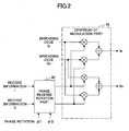
- Fig.2 is a block diagram of a demodulation apparatus corresponding to the modulation apparatus shown in Fig.1A. In Fig.2, 45 indicates a phase reverse rotation part and 46 indicates a despread demodulation part.
- the spread modulation part 11 has a transmit interrupt function (DXT) formed by AND gates A1-A4.
- the phase rotation part 12 is a part of a transmit diversity function for transmitting the same source information signals by shifting the phases.
- Fig. 1B shows constellations on a complex plain for the modulation apparatus.
- (b) shows a case where there is a phase rotation of 45° in which there are 9 signal points.
- the amplitude (2) of a signal output only on the I axis or only on the Q axis by the spread modulation part is two times of the amplitude (1) of other signal points. That is, 2 bits are necessary in a signal amplitude part. This results in increasing of the circuit size and the power consumption of the baseband modulation/demodulation apparatus.
- An object of the present invention is to provide digital baseband modulation/demodulation apparatuses for realizing high speed transmission while decreasing the size and the power consumption of the apparatuses.
- a digital baseband modulation apparatus including:
- the size (number of bits and the like) of the process circuits and transmit power consumption can be decreased.
- the size of the whole circuits can be downsized.
- a digital baseband demodulation apparatus including:
- the size (number of bits and the like) of the process circuits for air interface and receive power consumption can be decreased.
- the size of the whole circuits can be downsized.
- a digital baseband modulation apparatus of the present invention includes: a spread modulation part for complex spreading an I component signal and a Q component signal of a transmit signal by using spreading code for I axis and spreading code for Q axis so as to output an output signal comprising an output I component signal and an output Q component signal; and an amplitude conversion part for decreasing the amplitude component of the output signal to the half when the output signal is output on the I axis or on the Q axis.
- the spread modulation part may include a phase rotation part for rotating the phase angle of the output signal according to a control from the outside.
- transmit diversity can be efficiently realized by rotating the phase.
- a digital baseband demodulation apparatus of the present invention includes: a part for quadrature detecting an I component signal and a Q component signal from a received signal; an amplitude reverse conversion part for doubling the amplitude component of the received signal when the received signal is on the I axis or on the Q axis; and a despread demodulation part for complex despreading the I component signal and the Q component signal by using spreading code for I axis and spreading code for Q axis to obtain a complex despread signal.
- the despread demodulation part may include a phase rotation part for rotating the phase of the complex despread signal according to a control from the outside.
- receive diversity can be efficiently realized by rotating the phase.
- another digital baseband modulation apparatus of the present invention includes, as shown in Fig.8A, a plurality of pairs of the above-mentioned spread modulation part and the above-mentioned amplitude conversion part; a duplexing part for duplexing output signals output from the amplitude conversion parts by linearly adding the output signals; a separation part for separating a received high speed channel signal into a plurality of separated signals to be input into the spread modulation parts; and a switch part for switching between the separated signals and received low speed channel signals to input the separated signals or the received low speed channel signals into the spread modulation parts.
- Fig.8B shows a constellation of the signal output from the duplexing part 16. Since each amplitude component of signals output from the amplitude conversion parts on the I axis or on the Q axis are decreased to the half, the amplitude component of the duplexed signal is also decreased. Thus, the large capacity data transmission (HSDPA) can be realized with smaller circuit and lower power consumption.
- the duplexing part may add an offset value to each I component signal when the value of the I component signal is 0 and add an offset value to each Q component signal when the value of the Q component signal is 0. By adding the offset value to prevent I component or Q component from becoming 0. Accordingly, the process amount of a signal processing part can be decreased and dynamic range of a power amplifying part can be decreased.
- Fig.4 is a block diagram showing a part of a communication apparatus (for example, a mobile terminal) which is based on an embodiment of the present invention.
- 11 is a spread modulation part
- 12 is a phase rotation part
- 13 is an amplitude conversion part
- 31 is a D/A conversion part
- 32 is a quadrature modulation part (QMOD)
- 33 is a RF modulation part (TX) for up converting the quadrature modulated signal to the RF signal
- 34 is a transmit/receive wave switch part
- 35 is an antenna
- 41 is a RF demodulation part (RX) for down converting the received RF signal to the baseband signal
- 42 is a quadrature demodulation part (QDEM)
- 43 is an A/D conversion part
- 44 is an amplitude reverse conversion part
- 45 is a phase rotation part
- 46 is a despread demodulation part
- 47 is a detector part
- 48a and 48b show
- Figs.5A and 5B are block diagrams of the modulation/demodulation parts which are based on the first embodiment, in which a pair of the I component channel signal and the Q component signal is modulated/demodulated.
- Fig.5A is a block diagram of the modulation part.
- the modulation part includes the spread modulation part 11, the phase rotation part 12 and the amplitude conversion part 13 in which the amplitude conversion part 13 is provided at the back of the phase rotation part 12.
- Fig.5B is a block diagram of the demodulation part that includes the amplitude reverse conversion part 44, the phase reverse rotation part 45 and the despread demodulation part 46 in which the phase reverse rotation part 45 and the despread demodulation part 46 are provided behind the amplitude reverse conversion part 44.
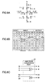
- Figs.6A-6C are diagrams for explaining the amplitude conversion part according to the first embodiment.
- Fig.6A shows constellations before and after performing the amplitude conversion process.
- the amplitude of the input signal on the I or Q axis takes one of three levels of (-2, 0, 2).
- the amplitude of other signals takes one of three levels of (-1, 0, 1).
- Fig.6B is a truth table used for the above-mentioned amplitude conversion process. As shown in the table, only when the amplitude component (I1, I0) or (Q1, Q0) of the input signal is (1, 0) or (0, 1), the amplitude component (I0) or (Q0) is converted to 1 and only the one bit is output. Accordingly, the amplitude component of the output signal can be reduced to 1 bit.
- Fig.6C is a logic circuit diagram that realizes the above truth table. As shown in the figure, the 1 bit sign of the input signal SI/SQ is output as it is. As to two bits amplitude components (I1, I0) and (Q1, Q0), EX-OR is calculated between I1 and I0, and between Q1 and Q0, so that amplitude of the output signal can be reduced to 1 bit amplitude component IO and Q0.
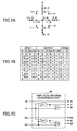
- Figs.7A-7C are diagrams for explaining the amplitude reverse conversion part which are based on the first embodiment.
- Fig.7A shows constellations before and after performing amplitude reverse conversion process.
- the amplitude of the input signal of the amplitude reverse part takes one of three levels of (-1, 0, 1) regardless whether the input signal is on the I/Q axis or not.
- Fig.7B is a truth table for realizing the above-mentioned amplitude reverse conversion process. As shown in the table, if (I0, Q0) is (1, 0) or (0, 1), amplitude component (I1, I0), (Q1, Q0) is converted to (1, 0), (0, 0) or (0, 0), (1, 0) respectively. Accordingly, the amplitude component of each of the I component signal and Q component signal can be reconstructed to two bits, that is, (I1, I0) or (Q1, Q0).
- Fig.7C is a logic circuit diagram for realizing the above truth table. As shown in the figure, 1 bit sign of input signal SI/SQ is output as it is. As to one bit amplitude component (I0) or (Q0), a logic shown in the figure is applied so that two bit amplitude component (I1, I0) or (Q1, Q0) can be reconstructed.
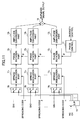
- Fig.8A is a block diagram of the modulation part which is based on the second embodiment of the present invention, in which signals of a plurality of channels each comprising a pair of I component signal and Q component signal are duplexed and transmitted.
- 11 1 -11 n are spread modulation parts
- 13 1 - 13 n are amplitude conversion parts
- 14 1 - 14 n are switches
- 15 is a serial to parallel conversion part (S/P) for separating an input signal of a high speed channel HSCH into signals of low speed channels
- 16 is a duplexing part for linearly adding (duplexing) output signals from the amplitude conversion parts 13 1 - 13 n .
- the modulation part accommodates n low speed channels CH1 - CHn for transmitting sounds and the like, and one high-speed channel HSCH for transmitting image data and the like.
- Each channel signal includes quadrature pair of the I component signal and the Q component signal.
- Fig.9 is a diagram for explaining a process for multiplexing signal points which is based on the second embodiment.
- Fig.9 shows a case in which I, Q data of two channels CH1 and CH2 are duplexed (linearly added).
- both amplitudes are 1, they cannot be distinguished from each other from the viewpoint of amplitude.
- phase rotation amounts of CH1 and CH2 are equally 0° or 45° (in phase synchronization), there is no combination other than the above-mentioned examples.
- phase rotation amounts of CH1 and CH2 are not the same (asynchronous), there are following combinations further.
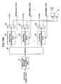
- Fig.10A is a block diagram of the demodulation part which is based on the second embodiment of the present invention, in which the demodulation part separates the duplexed received signal into a plurality of signals and demodulates each signal.
- 61 is an amplitude reverse conversion part for reverse converting the amplitude of the duplexed signal
- 62 is a hybrid for distributing signals after the amplitude reverse conversion
- 46 1 - 46 n are despread demodulation parts corresponding to each separated channel signal
- 63 1 -63 n are switches
- 64 is a parallel to serial conversion part (P/S).
- Fig.10B shows reverse conversion characteristics of the amplitude reverse conversion part. As shown in the figure, the input signal ( ⁇ N, 0) that exists only on I axis is reverse converted to ( ⁇ 2N, 0) and the input signal (0, ⁇ N) that exists only on Q axis is reverse converted to (0, ⁇ 2N), where N indicates the number of multiplexed channels.
- Fig.11 is a block diagram of a modulation part of the third embodiment, in which the modulation part has a transmit diversity function.
- 12 1 - 12 n are phase rotation parts
- 17 is a phase control part.
- phase rotation parts 12 1 - 12 n are provided for each channel, so that transmit diversity control can be performed. Thus, communication quality can be improved.
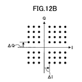
- Fig. 12A is a block diagram of a modulation part according to the fourth embodiment, in which a predetermined level offset is added to the output signal from the duplexing part. Following offset process is performed in the duplexing part 16. Predetermined offset values I and Q are added to I and Q levels respectively if the added result becomes a plus level (0 is considered to be +0). Other I and Q component signals are output as it is.
- the plus I component signal and the plus Q component signal are shifted to a plus direction in the above-mentioned example, a minus signal component may be shifted to a minus direction.
- the offset values can be added only when the level of the I component signal or the Q component signal is detected to be "0". In this case, whether the offset is added or not is sent to the receiving side.
- the present invention is not limited to this.
- the adder used for complex spread modulation can be removed from each spread modulation part 11, and add functions of the removed adders can be centered to an adder of the multiplexing part. Accordingly, the circuit size of the spread modulation parts can be decreased.
- the present invention since the size and the power consumption of the digital baseband modulation/demodulation apparatuses can be decreased, large capacity information can be transmitted efficiently at high speed. Thus, the present invention contributes to develop and popularize the next generation cellular phone system and the like.
Landscapes
- Engineering & Computer Science (AREA)
- Computer Networks & Wireless Communication (AREA)
- Signal Processing (AREA)
- Digital Transmission Methods That Use Modulated Carrier Waves (AREA)
- Amplitude Modulation (AREA)
Abstract
Description

Claims (7)
- A digital baseband modulation apparatus, comprising:a spread modulation part for complex spreading an I component signal and a Q component signal of a transmit signal by using spreading code for I axis and spreading code for Q axis so as to output an output signal comprising an output I component signal and an output Q component signal; andan amplitude conversion part for decreasing the amplitude component of the output signal to the half when the output signal is output on the I axis or on the Q axis.
- The digital baseband modulation apparatus as claimed in claim 1, wherein the spread modulation part comprises a phase rotation part for rotating the phase angle of the output signal according to a control from the outside.
- A digital baseband demodulation apparatus, comprising:a part for quadrature detecting an I component signal and a Q component signal from a received signal;an amplitude reverse conversion part for doubling the amplitude component of the received signal when the received signal is on the I,axis or on the Q axis; anda despread demodulation part for complex despreading the I component signal and the Q component signal by using spreading code for I axis and spreading code for Q axis to obtain a complex despread signal.
- The digital baseband demodulation apparatus as claimed in claim 3, the despread demodulation part further comprising a phase rotation part for rotating the phase of the complex despread signal according to a control from the outside.
- A digital baseband modulation apparatus, comprising a plurality of pairs of a spread modulation part and an amplitude conversion part, each pair receiving a transmit signal, wherein
the spread modulation part complex spreads an I component signal and a Q component signal of the transmit signal by using spreading code for I axis and spreading code for Q axis so as to output an output signal comprising an output I component signal and an output Q component signal; and
the amplitude conversion part decreases the amplitude component of the output signal to the half when the output signal is output on the I axis or on the Q axis;
the digital baseband modulation apparatus further comprising:a duplexing part for duplexing output signals output from the amplitude conversion parts by linearly adding the output signals;a separation part for separating a received high speed channel signal into a plurality of separated signals to be input into the spread modulation parts; anda switch part for switching between the separated signals and received low speed channel signals to input the separated signals or the received low speed channel signals into the spread modulation parts. - The digital baseband modulation apparatus as claimed in claim 5, wherein the duplexing part adds an offset value to each I component signal when the value of the I component signal is 0 and adds an offset value to each Q component signal when the value of the Q component signal is 0.
- A digital baseband demodulation apparatus, comprising:a part for quadrature detecting an I component signal and a Q component signal from a duplexed received signal;an amplitude reverse conversion part for doubling the amplitude component of the duplexed received signal when the duplexed received signal is on the I axis or on the Q axis;a part for separating the I component signal and the Q component signal output from the amplitude reverse conversion part into separated I component signals and separated Q component signals; anddespread demodulation parts for receiving each pair of the separated I component signals and separated Q component signals, each despread demodulation part complex despreading the pair by using spreading code for I axis and spreading code for Q axis.
Priority Applications (1)
| Application Number | Priority Date | Filing Date | Title |
|---|---|---|---|
| EP20060023540 EP1755232B1 (en) | 2003-01-29 | 2004-01-15 | Digital baseband modulation apparatus and demodulation apparatus |
Applications Claiming Priority (2)
| Application Number | Priority Date | Filing Date | Title |
|---|---|---|---|
| JP2003019986A JP4152205B2 (en) | 2003-01-29 | 2003-01-29 | Digital baseband modulator / demodulator |
| JP2003019986 | 2003-01-29 |
Related Child Applications (1)
| Application Number | Title | Priority Date | Filing Date |
|---|---|---|---|
| EP20060023540 Division EP1755232B1 (en) | 2003-01-29 | 2004-01-15 | Digital baseband modulation apparatus and demodulation apparatus |
Publications (3)
| Publication Number | Publication Date |
|---|---|
| EP1443670A2 true EP1443670A2 (en) | 2004-08-04 |
| EP1443670A3 EP1443670A3 (en) | 2004-10-20 |
| EP1443670B1 EP1443670B1 (en) | 2007-03-07 |
Family
ID=32652864
Family Applications (2)
| Application Number | Title | Priority Date | Filing Date |
|---|---|---|---|
| EP20060023540 Expired - Lifetime EP1755232B1 (en) | 2003-01-29 | 2004-01-15 | Digital baseband modulation apparatus and demodulation apparatus |
| EP20040000697 Expired - Lifetime EP1443670B1 (en) | 2003-01-29 | 2004-01-15 | Digital baseband modulation apparatus and demodulation apparatus |
Family Applications Before (1)
| Application Number | Title | Priority Date | Filing Date |
|---|---|---|---|
| EP20060023540 Expired - Lifetime EP1755232B1 (en) | 2003-01-29 | 2004-01-15 | Digital baseband modulation apparatus and demodulation apparatus |
Country Status (5)
| Country | Link |
|---|---|
| US (1) | US7545884B2 (en) |
| EP (2) | EP1755232B1 (en) |
| JP (1) | JP4152205B2 (en) |
| CN (1) | CN100490432C (en) |
| DE (2) | DE602004016053D1 (en) |
Families Citing this family (4)
| Publication number | Priority date | Publication date | Assignee | Title |
|---|---|---|---|---|
| CN101371464A (en) * | 2005-12-14 | 2009-02-18 | 艾利森电话股份有限公司 | On-Demand Despreading for Spread Spectrum Receivers |
| CN1988523B (en) * | 2005-12-21 | 2011-08-17 | 上海华虹集成电路有限责任公司 | Demodulating method and its circuit for amplitude modulation signal |
| US8059697B2 (en) * | 2008-07-02 | 2011-11-15 | Telefonaktiebolaget L M Ericsson (Publ) | Reduced peak-to-RMS ratio multicode signal |
| US8873603B2 (en) | 2011-08-01 | 2014-10-28 | Electronics And Telecommunications Research Institute | Method and apparatus for amplitude modulation of spread signal |
Family Cites Families (14)
| Publication number | Priority date | Publication date | Assignee | Title |
|---|---|---|---|---|
| FR2701178A1 (en) * | 1993-02-03 | 1994-08-05 | Philips Electronique Lab | Spread spectrum communication system with multiple users. |
| JP3311950B2 (en) | 1996-12-19 | 2002-08-05 | 富士通株式会社 | Code multiplex radio equipment |
| JP3311951B2 (en) | 1996-12-20 | 2002-08-05 | 富士通株式会社 | Code multiplex transmitter |
| US6266320B1 (en) * | 1998-04-08 | 2001-07-24 | Telefonaktiebolaget Lm Ericsson (Publ) | Amplitude limitation in CDMA system |
| JPH11331140A (en) * | 1998-05-15 | 1999-11-30 | Nec Eng Ltd | Frame synchronizing circuit |
| JP3031346B2 (en) * | 1998-08-19 | 2000-04-10 | 日本電気株式会社 | CDMA base station transmitting apparatus and serial signal transmitting method in CDMA base station transmitting apparatus |
| JP3362009B2 (en) | 1999-03-01 | 2003-01-07 | シャープ株式会社 | Spread spectrum communication equipment |
| JP4224168B2 (en) * | 1999-04-23 | 2009-02-12 | パナソニック株式会社 | Base station apparatus and peak power suppression method |
| EP2242192B1 (en) * | 1999-07-06 | 2018-09-12 | Samsung Electronics Co., Ltd. | Apparatus and method for encoding/decoding transport format combination indicator in CDMA mobile communication system |
| EP1484845B1 (en) * | 1999-09-14 | 2010-12-08 | Fujitsu Limited | CDMA receiver |
| US6535562B1 (en) * | 1999-11-30 | 2003-03-18 | Qualcomm Inc. | Method and apparatus for rotating the phase of a complex signal |
| US6421397B1 (en) * | 2000-01-28 | 2002-07-16 | Alcatel Canada Inc. | Modulation system having on-line IQ calibration |
| US7170952B2 (en) * | 2001-07-02 | 2007-01-30 | Powerwave Technologies, Inc. | System and method for post filtering peak power reduction in communications systems |
| KR100547843B1 (en) * | 2001-07-13 | 2006-02-01 | 삼성전자주식회사 | Transmission power control device and method for mobile communication system |
-
2003
- 2003-01-29 JP JP2003019986A patent/JP4152205B2/en not_active Expired - Fee Related
-
2004
- 2004-01-14 US US10/757,083 patent/US7545884B2/en not_active Expired - Fee Related
- 2004-01-15 DE DE200460016053 patent/DE602004016053D1/en not_active Expired - Lifetime
- 2004-01-15 EP EP20060023540 patent/EP1755232B1/en not_active Expired - Lifetime
- 2004-01-15 EP EP20040000697 patent/EP1443670B1/en not_active Expired - Lifetime
- 2004-01-15 DE DE200460005087 patent/DE602004005087T2/en not_active Expired - Lifetime
- 2004-01-19 CN CNB2004100027299A patent/CN100490432C/en not_active Expired - Fee Related
Also Published As
| Publication number | Publication date |
|---|---|
| CN100490432C (en) | 2009-05-20 |
| EP1443670B1 (en) | 2007-03-07 |
| EP1443670A3 (en) | 2004-10-20 |
| EP1755232B1 (en) | 2008-08-20 |
| DE602004016053D1 (en) | 2008-10-02 |
| EP1755232A1 (en) | 2007-02-21 |
| DE602004005087T2 (en) | 2007-11-08 |
| US20040146090A1 (en) | 2004-07-29 |
| US7545884B2 (en) | 2009-06-09 |
| JP2004235803A (en) | 2004-08-19 |
| JP4152205B2 (en) | 2008-09-17 |
| DE602004005087D1 (en) | 2007-04-19 |
| CN1520117A (en) | 2004-08-11 |
Similar Documents
| Publication | Publication Date | Title |
|---|---|---|
| US5737326A (en) | Multi-code code division multiple access receiver | |
| JP3830925B2 (en) | Constant amplitude binary quadrature modulation and demodulation device | |
| JP2737730B2 (en) | Spread spectrum transceiver | |
| US5583851A (en) | Mobile communication apparatus having multi-codes allocating function | |
| JP3003006B2 (en) | Method and apparatus for signal demodulation and diversity combining of quadrature modulated signals | |
| CN1107391C (en) | CDMA receiving apparatus | |
| US7031370B1 (en) | Spread-spectrum communication device | |
| US5910950A (en) | Demodulator phase correction for code division multiple access receiver | |
| US7545884B2 (en) | Digital baseband modulation apparatus and demodulation apparatus | |
| JP2001223614A (en) | Combiner | |
| KR20000022721A (en) | Method and apparatus for achieving demodulation in radio communications system using m-sequence orthogonal modulation | |
| US5724382A (en) | Multimode spread spectrum communication system tolerant to varying channel characteristics | |
| JP2002050982A (en) | Cdma reception equipment and its method | |
| JP2713269B2 (en) | Code multiplex communication equipment | |
| JP2974004B1 (en) | CDMA receiver and CDMA communication system | |
| KR20010027280A (en) | Parallel combinatory processing adaptive communication system and method for supporting multi-transmission rate | |
| JP3429716B2 (en) | Demodulation method and apparatus in wireless communication system using M-sequence quadrature modulation | |
| JP2928776B1 (en) | Spread spectrum communication equipment | |
| JPH10294716A (en) | Multi-code transmission method, transmitter and receiver, and multi-code transmission system | |
| JPH09284176A (en) | Spread spectrum transmitters and receivers | |
| KR100327415B1 (en) | Cdma receiver and method for controlling dynamic range thereof | |
| JPH09214466A (en) | Spread spectrum communication equipment | |
| KR20040095843A (en) | Constant amplitude coded bi-orthogonal coding and decoding apparatus | |
| JP2005130510A (en) | Multiple signal interference canceling apparatus and method in mobile communication system | |
| KR20000012197U (en) | Signal receiver |
Legal Events
| Date | Code | Title | Description |
|---|---|---|---|
| PUAI | Public reference made under article 153(3) epc to a published international application that has entered the european phase |
Free format text: ORIGINAL CODE: 0009012 |
|
| AK | Designated contracting states |
Kind code of ref document: A2 Designated state(s): AT BE BG CH CY CZ DE DK EE ES FI FR GB GR HU IE IT LI LU MC NL PT RO SE SI SK TR |
|
| AX | Request for extension of the european patent |
Extension state: AL LT LV MK |
|
| PUAL | Search report despatched |
Free format text: ORIGINAL CODE: 0009013 |
|
| AK | Designated contracting states |
Kind code of ref document: A3 Designated state(s): AT BE BG CH CY CZ DE DK EE ES FI FR GB GR HU IE IT LI LU MC NL PT RO SE SI SK TR |
|
| AX | Request for extension of the european patent |
Extension state: AL LT LV MK |
|
| 17P | Request for examination filed |
Effective date: 20041022 |
|
| 17Q | First examination report despatched |
Effective date: 20050209 |
|
| AKX | Designation fees paid |
Designated state(s): DE FR GB |
|
| GRAP | Despatch of communication of intention to grant a patent |
Free format text: ORIGINAL CODE: EPIDOSNIGR1 |
|
| GRAJ | Information related to disapproval of communication of intention to grant by the applicant or resumption of examination proceedings by the epo deleted |
Free format text: ORIGINAL CODE: EPIDOSDIGR1 |
|
| GRAP | Despatch of communication of intention to grant a patent |
Free format text: ORIGINAL CODE: EPIDOSNIGR1 |
|
| GRAS | Grant fee paid |
Free format text: ORIGINAL CODE: EPIDOSNIGR3 |
|
| RIN1 | Information on inventor provided before grant (corrected) |
Inventor name: SAWADA, KENSUKU |
|
| GRAA | (expected) grant |
Free format text: ORIGINAL CODE: 0009210 |
|
| AK | Designated contracting states |
Kind code of ref document: B1 Designated state(s): DE FR GB |
|
| REG | Reference to a national code |
Ref country code: GB Ref legal event code: FG4D |
|
| REF | Corresponds to: |
Ref document number: 602004005087 Country of ref document: DE Date of ref document: 20070419 Kind code of ref document: P |
|
| ET | Fr: translation filed | ||
| PLBE | No opposition filed within time limit |
Free format text: ORIGINAL CODE: 0009261 |
|
| STAA | Information on the status of an ep patent application or granted ep patent |
Free format text: STATUS: NO OPPOSITION FILED WITHIN TIME LIMIT |
|
| 26N | No opposition filed |
Effective date: 20071210 |
|
| REG | Reference to a national code |
Ref country code: FR Ref legal event code: PLFP Year of fee payment: 13 |
|
| REG | Reference to a national code |
Ref country code: FR Ref legal event code: PLFP Year of fee payment: 14 |
|
| REG | Reference to a national code |
Ref country code: FR Ref legal event code: PLFP Year of fee payment: 15 |
|
| PGFP | Annual fee paid to national office [announced via postgrant information from national office to epo] |
Ref country code: FR Payment date: 20171211 Year of fee payment: 15 |
|
| PGFP | Annual fee paid to national office [announced via postgrant information from national office to epo] |
Ref country code: DE Payment date: 20180103 Year of fee payment: 15 Ref country code: GB Payment date: 20180110 Year of fee payment: 15 |
|
| REG | Reference to a national code |
Ref country code: DE Ref legal event code: R119 Ref document number: 602004005087 Country of ref document: DE |
|
| GBPC | Gb: european patent ceased through non-payment of renewal fee |
Effective date: 20190115 |
|
| PG25 | Lapsed in a contracting state [announced via postgrant information from national office to epo] |
Ref country code: DE Free format text: LAPSE BECAUSE OF NON-PAYMENT OF DUE FEES Effective date: 20190801 Ref country code: FR Free format text: LAPSE BECAUSE OF NON-PAYMENT OF DUE FEES Effective date: 20190131 |
|
| PG25 | Lapsed in a contracting state [announced via postgrant information from national office to epo] |
Ref country code: GB Free format text: LAPSE BECAUSE OF NON-PAYMENT OF DUE FEES Effective date: 20190115 |