EP1443625A2 - Simple load driving circuit for driving plural loads in a given priority order - Google Patents
Simple load driving circuit for driving plural loads in a given priority order Download PDFInfo
- Publication number
- EP1443625A2 EP1443625A2 EP04000618A EP04000618A EP1443625A2 EP 1443625 A2 EP1443625 A2 EP 1443625A2 EP 04000618 A EP04000618 A EP 04000618A EP 04000618 A EP04000618 A EP 04000618A EP 1443625 A2 EP1443625 A2 EP 1443625A2
- Authority
- EP
- European Patent Office
- Prior art keywords
- load
- driving
- switching means
- switch
- terminal
- Prior art date
- Legal status (The legal status is an assumption and is not a legal conclusion. Google has not performed a legal analysis and makes no representation as to the accuracy of the status listed.)
- Granted
Links
Images
Classifications
-
- H—ELECTRICITY
- H03—ELECTRONIC CIRCUITRY
- H03K—PULSE TECHNIQUE
- H03K17/00—Electronic switching or gating, i.e. not by contact-making and –breaking
- H03K17/18—Modifications for indicating state of switch
-
- E—FIXED CONSTRUCTIONS
- E05—LOCKS; KEYS; WINDOW OR DOOR FITTINGS; SAFES
- E05F—DEVICES FOR MOVING WINGS INTO OPEN OR CLOSED POSITION; CHECKS FOR WINGS; WING FITTINGS NOT OTHERWISE PROVIDED FOR, CONCERNED WITH THE FUNCTIONING OF THE WING
- E05F15/00—Power-operated mechanisms for wings
- E05F15/60—Power-operated mechanisms for wings using electrical actuators
- E05F15/603—Power-operated mechanisms for wings using electrical actuators using rotary electromotors
- E05F15/665—Power-operated mechanisms for wings using electrical actuators using rotary electromotors for vertically-sliding wings
- E05F15/689—Power-operated mechanisms for wings using electrical actuators using rotary electromotors for vertically-sliding wings specially adapted for vehicle windows
- E05F15/695—Control circuits therefor
-
- H—ELECTRICITY
- H03—ELECTRONIC CIRCUITRY
- H03K—PULSE TECHNIQUE
- H03K17/00—Electronic switching or gating, i.e. not by contact-making and –breaking
- H03K17/002—Switching arrangements with several input- or output terminals
- H03K17/007—Switching arrangements with several input- or output terminals with several outputs only
-
- E—FIXED CONSTRUCTIONS
- E05—LOCKS; KEYS; WINDOW OR DOOR FITTINGS; SAFES
- E05Y—INDEXING SCHEME ASSOCIATED WITH SUBCLASSES E05D AND E05F, RELATING TO CONSTRUCTION ELEMENTS, ELECTRIC CONTROL, POWER SUPPLY, POWER SIGNAL OR TRANSMISSION, USER INTERFACES, MOUNTING OR COUPLING, DETAILS, ACCESSORIES, AUXILIARY OPERATIONS NOT OTHERWISE PROVIDED FOR, APPLICATION THEREOF
- E05Y2900/00—Application of doors, windows, wings or fittings thereof
- E05Y2900/50—Application of doors, windows, wings or fittings thereof for vehicles
- E05Y2900/53—Type of wing
- E05Y2900/55—Windows
Definitions
- the present invention relates to a load-driving circuit for driving loads such as motors, and more particularly, to a load-driving circuit capable of driving a plurality of loads based on a priority order endowed therewith.
- Japanese Unexamined Patent Application Publication No. 8-105270 is a power window apparatus with plural sets of driving devices, each having a power window motor and a power window switch for driving the power window motor, in which the operation of the power window switch with the highest priority order takes precedence, and the operation of the remaining switches is invalidated, when a plurality of the power window switches operates at the same time.
- the conventional power window apparatus described above is constructed with a microcomputer. Therefore, the apparatus can be driven in accordance with the predetermined order of priority given to the power window driving motors by the programs incorporated into the microcomputer. Furthermore, a control method thereof can be easily changed, thereby improving the convenience of use and scalability.
- the present invention has been designed to solve the above-described problems, and it is an object of.the present invention to provide a simple load-driving circuit capable of driving a plurality of loads based on a priority order endowed therewith.
- a load-driving circuit in accordance with one aspect of the present invention comprises the following components: a first load; a first driving switch for driving the first load; a second load; a second driving switch for driving the second load; first switching means being turned on when the first driving switch is switched to a position where the first load is driven; second switching means being turned on when the second driving switch is switched to a position where the second load is driven; and third switching means for ceasing driving the first load when the first switching means and the second switching means are turned on at the same time.
- a plurality of loads can be driven by a simple circuit based on the priority order endowed therewith.
- a load-driving circuit in accordance with another aspect of the present invention comprises the following components: a first motor; a first driving switch including a first switch connecting one terminal of the first motor to either a power supply terminal or a ground terminal, and a second switch connecting the other terminal of the first motor to either the power supply terminal or the ground terminal; a second motor; a second driving switch including a third switch connecting one terminal of the second motor to either the power supply terminal or the ground terminal, and a fourth switch connecting the other terminal of the second motor to either the power supply terminal to the ground terminal; first switching means being turned on when the first switch or the second switch operates; second switching means being turned on when the third switch or the fourth switch operates; and third switching means for disconnecting either terminal of the first motor from the power supply terminal or the ground terminal when the first switching means and the second switching means are turned on at the same time.
- a plurality of loads first and second motors capable of rotating in forward and reverse directions
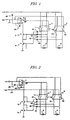
- Fig. 1 is a view illustrating a load-driving circuit according to an embodiment of the present invention.
- symbol +B designates a direct current source
- reference numeral 1 designates a first driving switch
- reference numeral 3 designates a first load including a motor driven by the first driving switch.
- the first driving switch 1 comprises a first changeover switch 11 that connects one end (one terminal) of the first load 3 to a terminal, of the direct current source +B, or to a ground terminal GND through third switching means 7, and a second changeover switch 12 that connects the other end (the other terminal) of the first load 3 to the terminal of the direct current source +B, or to the ground terminal GND through the third switching means 7.
- Reference numeral 2 designates a second driving switch
- reference numeral 4 designates a second load including a motor driven by the second driving switch.
- the second driving switch 2 comprises a third changeover switch 21 that connects one end (one terminal) of the second load 4 to either the terminal of the direct current source +B or the ground terminal GND, and a fourth changeover switch 22 that connects the other end (the other terminal) of the second load 4 to either the terminal of the direct current source +B or the ground terminal GND.
- Reference numeral 5 designates first switching means composed of a transistor and the like
- reference numeral 6 designates second switching means composed of a transistor and the like, which is connected in series to the first switching means 5
- reference numeral 7 designates third switching means composed of a relay and the like. Furthermore, the third switching means 7 is in an off state when the first switching means 5 and the second switching means 6 are in an on state.
- Reference numerals 41 and 42 designate diodes, which connect a base electrode of a transistor T1 constituting the first switching means to both terminals of the first load
- reference numerals 43 and 44 designate diodes, which connect a base electrode of a transistor T2 constituting the second switching means to both terminals of the second load
- Reference numerals 45 and 46 designate diodes
- reference numeral 47 designate an exciting coil of a relay constituting the third switching means.
- the base electrode of the transistor T1 constituting the first switching means 5 is supplied with a bias voltage through the diode 41 or the diode 42.
- the base electrode of the transistor T2 constituting the second switching means 6 is supplied with a bias voltage through the diode 43 or the diode 44.
- the transistor T1 constituting the first switching means 5 and the transistor T2 constituting the second switching means 6 are turned on at the same time. Consequently, the third switching means 7 is turned off, and thus one end of the first load 3 is disconnected from the ground terminal GND.
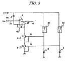
- Fig. 2 is a view illustrating a load-driving circuit according to another embodiment of the present invention.
- reference numeral T1 designates a transistor that constitutes the first switching means 5
- reference numeral T2 designates a transistor that constitutes the second switching means 6.
- NPN-type transistors have been employed as transistors constituting the first switching means 5 and the second switching means 6 in the aforementioned embodiment shown in Fig. 1, PNP-type transistors are employed for that purpose in the present embodiment.
- the diodes 41, 42, 43 and 44 are connected in the opposite direction to those in the above embodiment.
- the third switching means 7 is connected between either end of the first load 3 and the terminal of the direct current source +B. Because the operation of the circuit is the same as that of the above embodiment, a detailed description thereof is omitted.
- Fig. 3 is a view illustrating a load-driving circuit according to still another embodiment of the present invention.
- reference numeral 31 designates a first driving switch
- reference numeral 3 designates a first load such as a lamp driven by the first driving switch.
- the first driving switch 31 connects one end of the first load 3 to a direct current source +B.
- Reference numeral 32 designates a second driving switch
- reference numeral 4 designates a second load such as a lamp driven by the second switch.
- the second driving switch 32 connects one end of the second load 4 to the direct current source +B.
- Reference numeral 7 designates third switching means including a relay, which connects the other end of the first load 3 to the ground terminal GND.
- a base electrode of the transistor T1 constituting the first switching means 5 and one end of the first load 3 are connected to each other through a bias resistor R1.
- a base electrode of the transistor T2 constituting the second switching means 6 and one end of the second load 4 are connected to each other through a bias resistor R3.
- the parts that are the same as those depicted in Fig. 1 are designated with the same reference numerals, and a description thereof is omitted in order to avoid redundancy.
- the transistors T1 constituting the first switching means 5 and T2 constituting the second switching means 6 are turned on at the same time. Consequently, the third switching means is turned off, and thus one end of the first load 3 is disconnected from the ground terminal GND.
- a plurality of loads can be driven according to the priority order endowed therewith with a simple circuit and without using a microcomputer.
Landscapes
- Control Of Multiple Motors (AREA)
- Electronic Switches (AREA)
- Power-Operated Mechanisms For Wings (AREA)
- Window Of Vehicle (AREA)
- Logic Circuits (AREA)
Abstract
Description
Claims (2)
- A load-driving circuit comprising:a first load;a first driving switch for driving the first load;a second load;a second driving switch for driving the second load;first switching means being turned on when the first driving switch is switched to a position where the first load is driven;second switching means being turned on when the second driving switch is switched to a position where the second load is driven; andthird switching means for ceasing driving the first load when the first switching means and the second switching means are turned on at the same time.
- A motor driving circuit comprising:a first motor;a first driving switch including a first switch connecting one terminal of the first motor to either a power supply terminal or a ground terminal, and a second switch connecting the other terminal of the first motor to either the power supply terminal or the ground terminal;a second motor;a second driving switch including a third switch connecting one terminal of the second motor to either the power supply terminal or the ground terminal, and a fourth switch connecting the other terminal of the second motor to either the power supply terminal or the ground terminal;first switching means being turned on when the first switch or the second switch operates;second switching means being turned on when the third switch or the fourth switch operates; andthird switching means for disconnecting either terminal of the first motor from the power supply terminal or the ground terminal when the first switching means and the second switching means are turned on at the same time.
Applications Claiming Priority (2)
| Application Number | Priority Date | Filing Date | Title |
|---|---|---|---|
| JP2003012399A JP4160834B2 (en) | 2003-01-21 | 2003-01-21 | Load drive circuit |
| JP2003012399 | 2003-01-21 |
Publications (3)
| Publication Number | Publication Date |
|---|---|
| EP1443625A2 true EP1443625A2 (en) | 2004-08-04 |
| EP1443625A3 EP1443625A3 (en) | 2004-10-27 |
| EP1443625B1 EP1443625B1 (en) | 2006-03-29 |
Family
ID=32652808
Family Applications (1)
| Application Number | Title | Priority Date | Filing Date |
|---|---|---|---|
| EP04000618A Expired - Lifetime EP1443625B1 (en) | 2003-01-21 | 2004-01-14 | Simple load driving circuit for driving plural loads in a given priority order |
Country Status (4)
| Country | Link |
|---|---|
| US (1) | US6903522B2 (en) |
| EP (1) | EP1443625B1 (en) |
| JP (1) | JP4160834B2 (en) |
| DE (1) | DE602004000537T2 (en) |
Cited By (1)
| Publication number | Priority date | Publication date | Assignee | Title |
|---|---|---|---|---|
| DE102005058228A1 (en) * | 2005-11-11 | 2007-06-21 | Kia Motors Corporation | System for safely opening / closing a vehicle window with electric window lifter |
Family Cites Families (12)
| Publication number | Priority date | Publication date | Assignee | Title |
|---|---|---|---|---|
| DE204597C (en) | ||||
| JPS641722Y2 (en) * | 1979-07-30 | 1989-01-17 | ||
| US4349772A (en) * | 1980-12-23 | 1982-09-14 | General Electric Company | Method and apparatus for controlling an alternating current motor load using plural controlled-current inverter circuits |
| JPS59167276U (en) * | 1983-04-22 | 1984-11-09 | トヨタ自動車株式会社 | Vehicle power window device |
| DE3423830A1 (en) * | 1984-06-28 | 1986-01-02 | BURMEISTER Vertriebs- und Betreuungsgesellschaft mbH, 2900 Oldenburg | Circuit for limiting the maximum total power of a plurality of electrical loads |
| JP2798988B2 (en) * | 1989-07-28 | 1998-09-17 | 株式会社東芝 | Adjustable AC power supply for air conditioner |
| JP2674838B2 (en) * | 1989-08-23 | 1997-11-12 | アスモ株式会社 | Wind glass lifting device and window drive motor |
| JP2884942B2 (en) * | 1992-09-17 | 1999-04-19 | 株式会社日立製作所 | Electric car control device |
| JPH0835713A (en) * | 1994-07-26 | 1996-02-06 | Fujitsu General Ltd | Air conditioner control method and device |
| JP2853582B2 (en) | 1994-10-05 | 1999-02-03 | 住友電装株式会社 | Power window control method |
| IT1280496B1 (en) * | 1995-12-01 | 1998-01-20 | Magneti Marelli Climat Srl | CONTROL DEVICE FOR AN ELECTRIC WINDOW FOR VEHICLES. |
| JP3555567B2 (en) * | 2000-09-04 | 2004-08-18 | 日産自動車株式会社 | Control device for rotating electric machine |
-
2003
- 2003-01-21 JP JP2003012399A patent/JP4160834B2/en not_active Expired - Fee Related
-
2004
- 2004-01-14 EP EP04000618A patent/EP1443625B1/en not_active Expired - Lifetime
- 2004-01-14 DE DE602004000537T patent/DE602004000537T2/en not_active Expired - Lifetime
- 2004-01-16 US US10/759,329 patent/US6903522B2/en not_active Expired - Fee Related
Cited By (3)
| Publication number | Priority date | Publication date | Assignee | Title |
|---|---|---|---|---|
| DE102005058228A1 (en) * | 2005-11-11 | 2007-06-21 | Kia Motors Corporation | System for safely opening / closing a vehicle window with electric window lifter |
| DE102005058228B4 (en) * | 2005-11-11 | 2008-07-10 | Kia Motors Corporation | System for safely opening / closing a vehicle window with electric window lifter |
| US7605553B2 (en) | 2005-11-11 | 2009-10-20 | Kia Motor Corporation | System for safely opening/closing power window of vehicle |
Also Published As
| Publication number | Publication date |
|---|---|
| EP1443625A3 (en) | 2004-10-27 |
| DE602004000537T2 (en) | 2007-03-29 |
| US6903522B2 (en) | 2005-06-07 |
| US20040145329A1 (en) | 2004-07-29 |
| JP4160834B2 (en) | 2008-10-08 |
| JP2004229381A (en) | 2004-08-12 |
| DE602004000537D1 (en) | 2006-05-18 |
| EP1443625B1 (en) | 2006-03-29 |
Similar Documents
| Publication | Publication Date | Title |
|---|---|---|
| US20070152612A1 (en) | Motor controller | |
| EP0442688A2 (en) | Switching circuit | |
| US6903526B2 (en) | Electronically commutated DC motor comprising a bridge circuit | |
| JP4295389B2 (en) | Circuit and method for protection from overcurrent conditions and electrical no-load detection | |
| JPH08107632A (en) | Switching device | |
| US6429550B1 (en) | Polarity reversal protection circuit for a final electronic power stage | |
| US9209725B2 (en) | Motor drive circuit | |
| US6784687B2 (en) | Diagnostic device for electric mechanism drive circuits | |
| US6903522B2 (en) | Simple load-driving circuit capable of driving plural loads according to given priority order | |
| US20040165869A1 (en) | Speed control circuit for a brushless dc motor | |
| JP6724539B2 (en) | Load drive | |
| KR100260499B1 (en) | Structure of a selective calling receiver to connect with a vibration annunciator | |
| US10177761B2 (en) | Digital output circuit, printed-wiring board, and industrial apparatus | |
| JP3255927B2 (en) | Switching circuit with lockout characteristics | |
| KR970013619A (en) | Power transistor driving circuit in single power supply | |
| WO2023079975A1 (en) | Control device | |
| US5023493A (en) | FET and bipolar transistor bridge circuit for driving a load | |
| JP7310591B2 (en) | drive | |
| US20240421744A1 (en) | Motor drive circuit | |
| JP2010021818A (en) | Multifunctional driver circuit | |
| US7282817B2 (en) | Electrical circuit arrangement for controlling an electromotor in a motor vehicle | |
| US12105546B2 (en) | Control circuit and control unit for a vehicle | |
| JP2006197276A (en) | Simultaneous ON prevention circuit in relay drive | |
| CN117811558B (en) | High-side driving circuit, control method thereof and vehicle | |
| JP2000350494A (en) | Drive device for linear actuator |
Legal Events
| Date | Code | Title | Description |
|---|---|---|---|
| PUAI | Public reference made under article 153(3) epc to a published international application that has entered the european phase |
Free format text: ORIGINAL CODE: 0009012 |
|
| AK | Designated contracting states |
Kind code of ref document: A2 Designated state(s): AT BE BG CH CY CZ DE DK EE ES FI FR GB GR HU IE IT LI LU MC NL PT RO SE SI SK TR |
|
| AX | Request for extension of the european patent |
Extension state: AL LT LV MK |
|
| PUAL | Search report despatched |
Free format text: ORIGINAL CODE: 0009013 |
|
| AK | Designated contracting states |
Kind code of ref document: A3 Designated state(s): AT BE BG CH CY CZ DE DK EE ES FI FR GB GR HU IE IT LI LU MC NL PT RO SE SI SK TR |
|
| AX | Request for extension of the european patent |
Extension state: AL LT LV MK |
|
| RIC1 | Information provided on ipc code assigned before grant |
Ipc: 7E 05F 15/16 A Ipc: 7H 02P 7/00 B |
|
| 17P | Request for examination filed |
Effective date: 20050117 |
|
| 17Q | First examination report despatched |
Effective date: 20050324 |
|
| AKX | Designation fees paid |
Designated state(s): DE FR GB SE |
|
| GRAP | Despatch of communication of intention to grant a patent |
Free format text: ORIGINAL CODE: EPIDOSNIGR1 |
|
| GRAS | Grant fee paid |
Free format text: ORIGINAL CODE: EPIDOSNIGR3 |
|
| GRAA | (expected) grant |
Free format text: ORIGINAL CODE: 0009210 |
|
| AK | Designated contracting states |
Kind code of ref document: B1 Designated state(s): DE FR GB SE |
|
| REG | Reference to a national code |
Ref country code: GB Ref legal event code: FG4D |
|
| REF | Corresponds to: |
Ref document number: 602004000537 Country of ref document: DE Date of ref document: 20060518 Kind code of ref document: P |
|
| REG | Reference to a national code |
Ref country code: SE Ref legal event code: TRGR |
|
| ET | Fr: translation filed | ||
| PLBE | No opposition filed within time limit |
Free format text: ORIGINAL CODE: 0009261 |
|
| STAA | Information on the status of an ep patent application or granted ep patent |
Free format text: STATUS: NO OPPOSITION FILED WITHIN TIME LIMIT |
|
| 26N | No opposition filed |
Effective date: 20070102 |
|
| PGFP | Annual fee paid to national office [announced via postgrant information from national office to epo] |
Ref country code: GB Payment date: 20090123 Year of fee payment: 6 |
|
| PGFP | Annual fee paid to national office [announced via postgrant information from national office to epo] |
Ref country code: FR Payment date: 20090120 Year of fee payment: 6 |
|
| GBPC | Gb: european patent ceased through non-payment of renewal fee |
Effective date: 20100114 |
|
| REG | Reference to a national code |
Ref country code: FR Ref legal event code: ST Effective date: 20100930 |
|
| PG25 | Lapsed in a contracting state [announced via postgrant information from national office to epo] |
Ref country code: FR Free format text: LAPSE BECAUSE OF NON-PAYMENT OF DUE FEES Effective date: 20100201 |
|
| PG25 | Lapsed in a contracting state [announced via postgrant information from national office to epo] |
Ref country code: GB Free format text: LAPSE BECAUSE OF NON-PAYMENT OF DUE FEES Effective date: 20100114 |
|
| PGFP | Annual fee paid to national office [announced via postgrant information from national office to epo] |
Ref country code: DE Payment date: 20120131 Year of fee payment: 9 |
|
| PG25 | Lapsed in a contracting state [announced via postgrant information from national office to epo] |
Ref country code: DE Free format text: LAPSE BECAUSE OF NON-PAYMENT OF DUE FEES Effective date: 20130801 |
|
| REG | Reference to a national code |
Ref country code: DE Ref legal event code: R119 Ref document number: 602004000537 Country of ref document: DE Effective date: 20130801 |
|
| PGFP | Annual fee paid to national office [announced via postgrant information from national office to epo] |
Ref country code: SE Payment date: 20150108 Year of fee payment: 12 |
|
| PG25 | Lapsed in a contracting state [announced via postgrant information from national office to epo] |
Ref country code: SE Free format text: LAPSE BECAUSE OF NON-PAYMENT OF DUE FEES Effective date: 20160115 |