EP1443383A2 - Speed-matching control method and circuit - Google Patents
Speed-matching control method and circuit Download PDFInfo
- Publication number
- EP1443383A2 EP1443383A2 EP04250053A EP04250053A EP1443383A2 EP 1443383 A2 EP1443383 A2 EP 1443383A2 EP 04250053 A EP04250053 A EP 04250053A EP 04250053 A EP04250053 A EP 04250053A EP 1443383 A2 EP1443383 A2 EP 1443383A2
- Authority
- EP
- European Patent Office
- Prior art keywords
- chip
- signal
- frequency
- internal
- frequency signal
- Prior art date
- Legal status (The legal status is an assumption and is not a legal conclusion. Google has not performed a legal analysis and makes no representation as to the accuracy of the status listed.)
- Withdrawn
Links
Images


Classifications
-
- G—PHYSICS
- G06—COMPUTING OR CALCULATING; COUNTING
- G06F—ELECTRIC DIGITAL DATA PROCESSING
- G06F1/00—Details not covered by groups G06F3/00 - G06F13/00 and G06F21/00
- G06F1/04—Generating or distributing clock signals or signals derived directly therefrom
- G06F1/12—Synchronisation of different clock signals provided by a plurality of clock generators
Definitions
- the present invention relates to a method and apparatus for controlling and matching speeds of operation between different chips, especially for use in the design of circuitry for asynchronous inter-chip communications.
- the present invention provides apparatus and a method as set out in the appended claims.
- a system matches speeds of asynchronous operation between a local chip and a neighboring chip.
- the system derives an internal frequency signal from an internal oscillator on the local chip, and receives an external frequency signal from a neighboring chip.
- the system compares the internal frequency signal with the external frequency signal to generate a control signal, which is applied to the local chip to adjust the operating speed of the local chip.
- the control signal is also applied to the internal oscillator to adjust the frequency of the internal oscillator.
- adjusting the frequency of the local chip involves changing the power-supply voltage of the local chip.
- receiving the external frequency signal from the neighboring chip involves receiving the external frequency signal through a capacitor, an inductor, a resistor, a transmission line, or a direct contact.
- comparing the internal frequency signal with the external frequency signal involves converting the internal frequency signal and external frequency signal into corresponding current or voltage signals, which are proportional to the frequencies of the frequency signals.
- the system converts the internal frequency signal and the external frequency signal into corresponding current signals, and then compares the two current signals to generate a difference current signal.
- the difference current signal is then coupled to an integrating capacitor to produce an integrated voltage signal.
- the system also applies an offset current source to the integrating capacitor to compensate for transistor leakages, parasitics, and/or nonlinearities.
- the system further includes an amplifier which is coupled to the integrating capacitor. The input to the amplifier is the integrated voltage signal and the output of the amplifier is the control signal.
- the system filters the control signal to improve matching between the local chip's operating speed and the neighboring chip's operating speed.
- filtering the control signal involves coupling a filter capacitor between the control signal and ground.
- the internal frequency signal has a frequency that is a fraction of the internal oscillator frequency of the local node
- the external frequency signal has a frequency that is a fraction of an external oscillator frequency of the neighboring node.
- FIG. 1 illustrates a speed control circuit in accordance with one embodiment of the present invention.
- chips 130 and 140 contain the same speed control circuits, which are coupled together to form a loop.
- Chips 130 and 140 are coupled together through capacitors 105 and 106.
- they can be coupled through any type of connection, for instance a resistor, an inductor, a transmission line, or just a simple wire.
- Each half of the speed control loop comprises two parts: a variable frequency oscillator with a control input, and a frequency detector circuit 110. Additionally, there may be filtering elements, such as capacitors, resistors, or inductors, which are used to improve the stability, response time, and/or performance of the control loop. For example, in FIG. 1, a filter capacitor 103 is shown coupled to V ctl to smooth out ripples on the control voltages. Note that the frequency detector circuit can additionally include an internal integrating capacitor to improve the loop stability of the overall speed control loop.
- the speed control loop operates as follows.
- the oscillator on each chip is designed to operate just below the chip's maximum operating speed when the control voltage input is at its maximum speed setting.
- the connections between chips transmit a signal whose frequency is the frequency of the oscillator.
- Each chip compares its internal oscillator frequency against the frequency transmitted by the other chip and, if necessary, slows down or speeds up its internal frequency to match the frequency of the other chip.
- the response time of these frequency corrections needs to be slow in comparison with delay involved in sending signals between chips to make the overall control loop stable.
- Each chip starts by transmitting its maximum frequency.
- the slower chip will be unable to go any faster and its oscillator will simply continue to oscillate at the maximum speed.
- the faster chip will slow down to match the speed of the slower chip.
- the local oscillator is comprised of NAND gate 102 and a number of cascaded inverters, such as inverter 101.
- the cascaded inverters are coupled to the inputs of NAND gate 102, wherein distribution of inverters on each input of NAND gate 102 determines the duty cycle of the generated timing signal.
- the oscillator frequency is determined by the delays of inverters. Note that the delays of these inverters and NAND gate 101 can be controlled by varying the voltage of their power supply. Hence, by varying a common power-supply voltage, V ctl , one can adjust the frequency of the timing signal generated by the oscillator.
- FIG. 2 illustrates a frequency detector circuit in accordance with one embodiment of the present invention.
- This frequency detector first converts the frequency of each input signal into a current signal that is proportional to the respective signal's frequency. It then integrates the current signals on a capacitor. Finally the integrated voltage is buffered by an amplifier before being used to adjust the internal oscillator frequency and the chip's operating speed. Note that this integration can help to provide control loop stability.
- V out K FD ( Freq1 - Freq2 ) wherein Freq1 and Freq2 are two input frequencies, and K FD is a constant.
- frequency 1 and frequency 2 there are two input frequency signals: frequency 1 and frequency 2. These input frequency signals feed into respective edge detector circuits comprised of cascaded invertors and NAND gates. Each of these edge detector circuits produces a low voltage pulse on a rising edge of the input frequency signal. This configuration allows the output pulse signal's frequency to be proportional to the frequency of the input signal while the pulse width is independent of the input signal's duty cycle. This is because the width of the pulse is determined only by the delays of the inverters.
- frequency 1 is converted to a downward pulsed signal V edge1
- frequency 2 is converted to an upward pulsed signal V edge2 with an additional inverter 210.
- V edge1 is then coupled to the gate of PMOS transistor 203, the source of which is connected to current source 201.
- the purpose of this configuration is to turn on PMOS transistor 203 and to let a current flow into the drain of PMOS transistor 203 for the duration of the pulse whenever there is a rising edge in the input signal, frequency 1.
- V edge2 is coupled to the gate of NMOS transistor 204, the source of which is connected to current source 202, such that whenever there is a rising edge in frequency 2, NMOS transistor 202 is turned on and a current flows out of the drain of NMOS transistor 202.
- the circuit further includes an integrating capacitor 206.
- the voltage that appears across capacitor 206 reflects the time integral of the difference current signal.
- V ctl The final output of the frequency detector circuit, V ctl , is obtained from an operational amplifier (OP AMP) 207 configured as a unity-gain amplifier, wherein the input of the unity-gain amplifier is the voltage produced by integrating capacitor 206. V ctl is then used to adjust both the internal oscillator frequency and the operating speed of the asynchronous chip.
- OP AMP operational amplifier
- control loop may successively increase an oscillator's frequency to be just slightly higher than the other chip's frequency, and stop when the slower chip's oscillator hits its maximum frequency. At that point, the control loop is nonlinear, and the faster chip will operate just a bit faster than that frequency.
- the offset current causes frequency 1 signal to cycle slightly faster than the frequency 2 signal when the speed control loop is locked. This is important to prevent a certain error mode where both chips would try to go slightly more slowly than each other, and would eventually slow down to a complete stop.
- biasing the frequency detector circuit one can make each chip try to cycle slightly faster than the other. What happens is that the slow chip operates at its maximum frequency (because its control loop is pegged against its maximum speed of operation) and the fast chip operates slightly faster than that.
- the frequency broadcast should be slightly slower than the chip's maximum speed of operation. For example, if the offset current causes the frequency control loop to attempt to operate 1 % faster than the other chip, then the frequencies broadcast should be at least 1 % slower than the chips' maximum frequencies.
- the slower chip may not be able to recognize the faster chip's frequency. Instead, the slower chip may mistake the faster chip's frequency signal for a DC signal. In this case, the slower chip will initially slow down its speed. This, however, is acceptable, because the faster chip will slow down its speed of operation. Eventually the faster chip will slow down enough such that the slower chip can correctly recognize the faster chip's frequency. At this point the control loop will operate correctly and the slower chip's oscillator will speed back up to its maximum speed of operation.
- An alternative to transmitting a chip's full oscillating frequency to other chips is transmitting a frequency that is a fraction of the chip's full oscillating frequency, wherein this transmitted frequency is proportional to the full oscillating frequency via a factor K .
- the frequency detector circuit in a receiving chip generates a V ctl that makes its oscillator operate at a frequency that is (approximately) K times as fast as the detected external frequency.
- FIG. 3A shows an example waveform of an input frequency signal coupled to the "frequency 1" input in FIG. 2.
- FIG. 3B shows the waveform at V edge1 .
- the pulse of V edge1 is a downward pulse, and the starting (falling) edge of a pulse corresponds to a rising edge of the input frequency signal.
- the pulse width is independent of the duty cycle of the input frequency signal.
- FIG. 3C shows an example waveform of an input frequency signal coupled to the "frequency 2" input in FIG. 2.
- FIG. 3D shows the waveform at V edge2 .
- the pulse of V edge2 is an upward pulse, and the starting (rising) edge of a pulse corresponds to a rising edge of the input frequency signal.
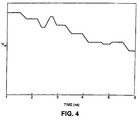
- FIG. 4 illustrates an example waveform of the output control voltage (V ctl ) from a frequency detector in accordance with one embodiment of the present invention.
- V ctl is slowing down the local oscillator to match the speed of a slower chip.
Landscapes
- Engineering & Computer Science (AREA)
- Theoretical Computer Science (AREA)
- Physics & Mathematics (AREA)
- General Engineering & Computer Science (AREA)
- General Physics & Mathematics (AREA)
- Stabilization Of Oscillater, Synchronisation, Frequency Synthesizers (AREA)
Abstract
Description
Claims (16)
- A method for matching speeds of asynchronous operation between a local chip (130) and a neighboring chip (140), the method comprising:deriving an internal frequency signal from an internal oscillator on the local chip;receiving an external frequency signal from a neighboring chip;comparing the internal frequency signal with the external frequency signal to generate a control signal;adjusting the operating speed of the local chip by applying the control signal to the local chip; andadjusting the frequency of the internal oscillator by applying the control signal to the internal oscillator.
- The method of claim 1, wherein adjusting the operating speed of the local chip involves changing the power-supply voltage of the local chip.
- The method of claim 1 or 2, wherein comparing the internal frequency signal with the external frequency signal involves converting the internal frequency signal and external frequency signal into corresponding current or voltage signals that are proportional to the frequencies of the internal and external frequency signals.
- The method of claim 3,
wherein the internal frequency signal and the external frequency signal are converted into corresponding current signals;
wherein comparing the internal frequency signal with the external frequency signal involves comparing the two current signals to generate a difference current signal; and
wherein the method further comprises:coupling the difference current signal to an integrating capacitor (206) to produce an integrated voltage signal;applying an offset current source (205) to the integrating capacitor; andcoupling the integrating capacitor to an amplifier (207), wherein the input to the amplifier is the integrated voltage signal and the output of the amplifier is the control signal. - The method of any preceding claim, further comprising filtering the control signal to improve matching between the local chip's operating speed and the neighboring chip's operating speed.
- The method of claim 5, wherein filtering the control signal involves coupling a filter capacitor (103) between the control signal and ground.
- The method of any preceding claim, whereinthe internal frequency signal has a frequency that is a fraction of the internal oscillator frequency of the local node; and whereinthe external frequency signal has a frequency that is a fraction of an external oscillator frequency of the neighboring node.
- Apparatus for matching speeds of asynchronous operation between a local chip (130) and a neighboring chip (140), the apparatus comprising:an internal oscillator on the local chip, from which an internal frequency signal can be derived;a receiving mechanism configured to receive an external frequency signal from a neighboring chip;a comparison mechanism (110) configured to compare the internal frequency signal with the external frequency signal to generate a control signal; andan adjusting mechanism configured to adjust the operating speed of the local chip and the internal oscillator by applying the control signal to the local chip and the internal oscillator.
- The apparatus of claim 8, wherein the adjusting mechanism is configured to adjust the operating speed of the local chip by changing the power-supply voltage of the local chip.
- The apparatus of claim 8 or 9, wherein the receiving mechanism is configured to receive the external frequency signal from the neighboring chip through a capacitor (105), an inductor, a resistor, a transmission line, or a direct contact.
- The apparatus of any of claims 8 to 10, wherein the comparison mechanism is configured to convert the internal frequency signal and the external frequency signal into corresponding current or voltage signals that are proportional to the frequencies of the internal and external frequency signals.
- The apparatus of claim 11,
wherein the external frequency signal and the internal frequency signal are converted into corresponding current signals;
wherein the comparison mechanism is configured to compare the two current signals to generate a difference current signal; and
wherein the apparatus further comprises:an integrating capacitor (206) to which the difference current signal is coupled to produce an integrated voltage signal;an offset current source (205) applied to the integrating capacitor; andan amplifier (207) to which the integrating capacitor is coupled, wherein the input to the amplifier is the integrated voltage signal and the output of the amplifier is the control signal. - The apparatus of any of claims 8 to 12, further comprising a filtering mechanism configured to filter the control signal to improve matching between the local chip's operating speed and the neighboring chip's operating speed.
- The apparatus of claim 13, wherein the filtering mechanism includes a filter capacitor (103) coupled between the control signal and ground.
- The apparatus of any of claims 8 to 14, whereinthe internal frequency signal has a frequency that is a fraction of the internal oscillator frequency of the local node; and whereinthe external frequency signal has a frequency that is a fraction of an external oscillator frequency of the neighboring node.
- A computer system comprising:a central processing unit;a semiconductor memory; anda circuit for matching speeds of asynchronous operation between a local chip and a neighboring chip, said circuit comprising the apparatus of any of claims 8 to 15.
Applications Claiming Priority (4)
| Application Number | Priority Date | Filing Date | Title |
|---|---|---|---|
| US44359103P | 2003-01-29 | 2003-01-29 | |
| US443591P | 2003-01-29 | ||
| US671641 | 2003-09-26 | ||
| US10/671,641 US7256628B2 (en) | 2003-01-29 | 2003-09-26 | Speed-matching control method and circuit |
Publications (2)
| Publication Number | Publication Date |
|---|---|
| EP1443383A2 true EP1443383A2 (en) | 2004-08-04 |
| EP1443383A3 EP1443383A3 (en) | 2006-09-06 |
Family
ID=32659510
Family Applications (1)
| Application Number | Title | Priority Date | Filing Date |
|---|---|---|---|
| EP04250053A Withdrawn EP1443383A3 (en) | 2003-01-29 | 2004-01-07 | Speed-matching control method and circuit |
Country Status (4)
| Country | Link |
|---|---|
| US (1) | US7256628B2 (en) |
| EP (1) | EP1443383A3 (en) |
| JP (1) | JP2004236326A (en) |
| TW (1) | TWI249288B (en) |
Cited By (1)
| Publication number | Priority date | Publication date | Assignee | Title |
|---|---|---|---|---|
| US7256628B2 (en) | 2003-01-29 | 2007-08-14 | Sun Microsystems, Inc. | Speed-matching control method and circuit |
Families Citing this family (7)
| Publication number | Priority date | Publication date | Assignee | Title |
|---|---|---|---|---|
| JP4246141B2 (en) * | 2004-03-22 | 2009-04-02 | シャープ株式会社 | Data processing device |
| KR100688530B1 (en) * | 2005-02-12 | 2007-03-02 | 삼성전자주식회사 | Operation speed detection device and operation speed detection method |
| KR101003153B1 (en) * | 2009-05-15 | 2010-12-21 | 주식회사 하이닉스반도체 | Voltage stabilization circuit and semiconductor memory device using same |
| US8907707B2 (en) | 2013-03-01 | 2014-12-09 | Laurence H. Cooke | Aligning multiple chip input signals using digital phase lock loops |
| US8593191B1 (en) | 2013-03-01 | 2013-11-26 | Laurence H. Cooke | Aligning multiple chip input signals using digital phase lock loops |
| US9413364B2 (en) | 2014-07-09 | 2016-08-09 | Intel Corporation | Apparatus and method for clock synchronization for inter-die synchronized data transfer |
| CN105634445B (en) * | 2015-12-28 | 2018-07-31 | 北京时代民芯科技有限公司 | A kind of configurable pierce circuit of frequency applied to Switching Power Supply |
Family Cites Families (22)
| Publication number | Priority date | Publication date | Assignee | Title |
|---|---|---|---|---|
| US4151473A (en) * | 1977-11-18 | 1979-04-24 | Harris Corporation | Phase detector circuit |
| US4239982A (en) * | 1978-06-14 | 1980-12-16 | The Charles Stark Draper Laboratory, Inc. | Fault-tolerant clock system |
| US4383216A (en) | 1981-01-29 | 1983-05-10 | International Business Machines Corporation | AC Measurement means for use with power control means for eliminating circuit to circuit delay differences |
| AU549343B2 (en) | 1981-06-08 | 1986-01-23 | British Telecommunications Public Limited Company | Phase locking |
| US4495594A (en) * | 1981-07-01 | 1985-01-22 | International Business Machines Corporation | Synchronization of CRT controller chips |
| US4635186A (en) * | 1983-06-20 | 1987-01-06 | International Business Machines Corporation | Detection and correction of multi-chip synchronization errors |
| US4902986B1 (en) | 1989-01-30 | 1998-09-01 | Credence Systems Corp | Phased locked loop to provide precise frequency and phase tracking of two signals |
| EP0560525B1 (en) * | 1992-03-11 | 1997-10-15 | Matsushita Electric Industrial Co., Ltd. | Frequency synthesizer |
| US5631591A (en) * | 1995-05-30 | 1997-05-20 | National Semiconductor Corporation | Method and apparatus for synchronizing timing signals of two integrated circuit chips |
| US6112308A (en) * | 1998-01-23 | 2000-08-29 | Intel Corporation | Cascaded multiple internal phase-locked loops for synchronization of hierarchically distinct chipset components and subsystems |
| US6009532A (en) * | 1998-01-23 | 1999-12-28 | Intel Corporation | Multiple internal phase-locked loops for synchronization of chipset components and subsystems |
| US6208183B1 (en) * | 1999-04-30 | 2001-03-27 | Conexant Systems, Inc. | Gated delay-locked loop for clock generation applications |
| US6194969B1 (en) * | 1999-05-19 | 2001-02-27 | Sun Microsystems, Inc. | System and method for providing master and slave phase-aligned clocks |
| US6757350B1 (en) * | 1999-06-12 | 2004-06-29 | Cisco Technology, Inc. | Redundant clock generation and distribution |
| US6239626B1 (en) * | 2000-01-07 | 2001-05-29 | Cisco Technology, Inc. | Glitch-free clock selector |
| US6297702B1 (en) * | 2000-01-10 | 2001-10-02 | Honeywell International Inc. | Phase lock loop system and method |
| US6973145B1 (en) * | 2000-09-01 | 2005-12-06 | Ut-Battelle, Llc | Digital-data receiver synchronization method and apparatus |
| US6346838B1 (en) * | 2001-01-05 | 2002-02-12 | Taiwan Semiconductor Manufacturing Corporation | Internal offset-canceled phase locked loop-based deskew buffer |
| US6538516B2 (en) * | 2001-05-17 | 2003-03-25 | Fairchild Semiconductor Corporation | System and method for synchronizing multiple phase-lock loops or other synchronizable oscillators without using a master clock signal |
| US6489821B1 (en) * | 2001-08-28 | 2002-12-03 | Intel Corporation | High frequency system with duty cycle buffer |
| JP2003198339A (en) * | 2001-12-21 | 2003-07-11 | Mitsubishi Electric Corp | Semiconductor device |
| US7256628B2 (en) | 2003-01-29 | 2007-08-14 | Sun Microsystems, Inc. | Speed-matching control method and circuit |
-
2003
- 2003-09-26 US US10/671,641 patent/US7256628B2/en not_active Expired - Lifetime
-
2004
- 2004-01-07 EP EP04250053A patent/EP1443383A3/en not_active Withdrawn
- 2004-01-28 JP JP2004020596A patent/JP2004236326A/en not_active Withdrawn
- 2004-01-29 TW TW093102023A patent/TWI249288B/en not_active IP Right Cessation
Cited By (1)
| Publication number | Priority date | Publication date | Assignee | Title |
|---|---|---|---|---|
| US7256628B2 (en) | 2003-01-29 | 2007-08-14 | Sun Microsystems, Inc. | Speed-matching control method and circuit |
Also Published As
| Publication number | Publication date |
|---|---|
| US20040145395A1 (en) | 2004-07-29 |
| JP2004236326A (en) | 2004-08-19 |
| EP1443383A3 (en) | 2006-09-06 |
| TWI249288B (en) | 2006-02-11 |
| TW200419913A (en) | 2004-10-01 |
| US7256628B2 (en) | 2007-08-14 |
Similar Documents
| Publication | Publication Date | Title |
|---|---|---|
| US5642082A (en) | Loop filter level detection circuit and method | |
| US5359727A (en) | Clock generator using PLL and information processing system using the clock generator | |
| US7015721B2 (en) | Push-pull output driver | |
| US20080258700A1 (en) | Method and apparatus for adjusting on-chip delay with power supply control | |
| JPS62234415A (en) | High speed switching charge pump | |
| US7352755B2 (en) | Network interface card (NIC) with phase lock rise time control generating circuit | |
| KR960027337A (en) | Positive logic circuit with improved output signal level | |
| US7106114B2 (en) | Delay time adjusting method of delaying a phase of an output signal until a phase difference between an input signal and the output signal becomes an integral number of periods other than zero | |
| US5638019A (en) | Accurately generating precisely skewed clock signals | |
| JP2025078717A (en) | Pulse signal transmission circuit | |
| US7256628B2 (en) | Speed-matching control method and circuit | |
| US7061290B2 (en) | PLL circuit with simulation components to reduce phase offset | |
| KR19990078246A (en) | Charge pump circuit for PLL | |
| US6414517B1 (en) | Input buffer circuits with input signal boost capability and methods of operation thereof | |
| US6246294B1 (en) | Supply noise immunity low-jitter voltage-controlled oscillator design | |
| US6891411B2 (en) | Low injection charge pump | |
| US6642761B1 (en) | Interface circuit of various clock period between a fast slope signal and a very slow slope, voltage controlled delay cell | |
| US6232813B1 (en) | Phase locked loop integrated circuits having fuse-enabled and fuse-disabled delay devices therein | |
| JP2001044813A (en) | Power-on reset circuit | |
| US20030128065A1 (en) | Circuit assembly for converting a differential input clock signal pair into a single-ended output clock signal | |
| CN110719103B (en) | Integrated circuit including phase-locked loop circuit | |
| US20160241233A1 (en) | Driver circuit for single wire protocol slave unit | |
| JPH07115351A (en) | Delay circuit, signal processing circuit using the same, and semiconductor integrated circuit device incorporating the signal processing circuit | |
| WO1997009811A1 (en) | Low jitter low power single ended driver | |
| KR0146192B1 (en) | Charging pump for driving high current |
Legal Events
| Date | Code | Title | Description |
|---|---|---|---|
| PUAI | Public reference made under article 153(3) epc to a published international application that has entered the european phase |
Free format text: ORIGINAL CODE: 0009012 |
|
| AK | Designated contracting states |
Kind code of ref document: A2 Designated state(s): AT BE BG CH CY CZ DE DK EE ES FI FR GB GR HU IE IT LI LU MC NL PT RO SE SI SK TR |
|
| AX | Request for extension of the european patent |
Extension state: AL LT LV MK |
|
| PUAL | Search report despatched |
Free format text: ORIGINAL CODE: 0009013 |
|
| AK | Designated contracting states |
Kind code of ref document: A3 Designated state(s): AT BE BG CH CY CZ DE DK EE ES FI FR GB GR HU IE IT LI LU MC NL PT RO SE SI SK TR |
|
| AX | Request for extension of the european patent |
Extension state: AL LT LV MK |
|
| AKX | Designation fees paid | ||
| REG | Reference to a national code |
Ref country code: DE Ref legal event code: 8566 |
|
| STAA | Information on the status of an ep patent application or granted ep patent |
Free format text: STATUS: THE APPLICATION IS DEEMED TO BE WITHDRAWN |
|
| 18D | Application deemed to be withdrawn |
Effective date: 20070307 |