EP1442328B1 - Optical fiber array block embedding optical device therein - Google Patents
Optical fiber array block embedding optical device therein Download PDFInfo
- Publication number
- EP1442328B1 EP1442328B1 EP02790959A EP02790959A EP1442328B1 EP 1442328 B1 EP1442328 B1 EP 1442328B1 EP 02790959 A EP02790959 A EP 02790959A EP 02790959 A EP02790959 A EP 02790959A EP 1442328 B1 EP1442328 B1 EP 1442328B1
- Authority
- EP
- European Patent Office
- Prior art keywords
- optical
- block
- intermediate panel
- leakage
- optical fiber
- Prior art date
- Legal status (The legal status is an assumption and is not a legal conclusion. Google has not performed a legal analysis and makes no representation as to the accuracy of the status listed.)
- Expired - Lifetime
Links
- 230000003287 optical effect Effects 0.000 title claims abstract description 169
- 239000013307 optical fiber Substances 0.000 title claims abstract description 76
- 239000000758 substrate Substances 0.000 claims description 28
- 239000003292 glue Substances 0.000 claims description 7
- 229910000679 solder Inorganic materials 0.000 claims description 4
- 239000000463 material Substances 0.000 claims description 3
- 230000000149 penetrating effect Effects 0.000 claims description 3
- 238000012545 processing Methods 0.000 claims description 3
- 239000000835 fiber Substances 0.000 claims 1
- 150000002500 ions Chemical class 0.000 claims 1
- 238000000034 method Methods 0.000 abstract description 12
- 238000005468 ion implantation Methods 0.000 abstract 1
- 238000004891 communication Methods 0.000 description 6
- 238000013459 approach Methods 0.000 description 5
- 238000009826 distribution Methods 0.000 description 5
- 230000005540 biological transmission Effects 0.000 description 2
- 230000008878 coupling Effects 0.000 description 2
- 238000010168 coupling process Methods 0.000 description 2
- 238000005859 coupling reaction Methods 0.000 description 2
- 238000005520 cutting process Methods 0.000 description 2
- 238000001514 detection method Methods 0.000 description 2
- 238000010586 diagram Methods 0.000 description 2
- 239000012535 impurity Substances 0.000 description 2
- 230000002265 prevention Effects 0.000 description 2
- 230000001902 propagating effect Effects 0.000 description 2
- RZVAJINKPMORJF-UHFFFAOYSA-N Acetaminophen Chemical compound CC(=O)NC1=CC=C(O)C=C1 RZVAJINKPMORJF-UHFFFAOYSA-N 0.000 description 1
- 239000011149 active material Substances 0.000 description 1
- 150000001875 compounds Chemical class 0.000 description 1
- 230000001808 coupling effect Effects 0.000 description 1
- 239000011521 glass Substances 0.000 description 1
- 230000006698 induction Effects 0.000 description 1
- 238000003780 insertion Methods 0.000 description 1
- 230000037431 insertion Effects 0.000 description 1
- 239000007791 liquid phase Substances 0.000 description 1
- 238000004519 manufacturing process Methods 0.000 description 1
- 238000005259 measurement Methods 0.000 description 1
- 239000005297 pyrex Substances 0.000 description 1
- 229910052710 silicon Inorganic materials 0.000 description 1
- 239000010703 silicon Substances 0.000 description 1
- 238000003892 spreading Methods 0.000 description 1
Images



Classifications
-
- G—PHYSICS
- G02—OPTICS
- G02B—OPTICAL ELEMENTS, SYSTEMS OR APPARATUS
- G02B6/00—Light guides; Structural details of arrangements comprising light guides and other optical elements, e.g. couplings
- G02B6/24—Coupling light guides
- G02B6/42—Coupling light guides with opto-electronic elements
-
- G—PHYSICS
- G02—OPTICS
- G02B—OPTICAL ELEMENTS, SYSTEMS OR APPARATUS
- G02B6/00—Light guides; Structural details of arrangements comprising light guides and other optical elements, e.g. couplings
- G02B6/24—Coupling light guides
- G02B6/26—Optical coupling means
- G02B6/28—Optical coupling means having data bus means, i.e. plural waveguides interconnected and providing an inherently bidirectional system by mixing and splitting signals
- G02B6/2804—Optical coupling means having data bus means, i.e. plural waveguides interconnected and providing an inherently bidirectional system by mixing and splitting signals forming multipart couplers without wavelength selective elements, e.g. "T" couplers, star couplers
- G02B6/2852—Optical coupling means having data bus means, i.e. plural waveguides interconnected and providing an inherently bidirectional system by mixing and splitting signals forming multipart couplers without wavelength selective elements, e.g. "T" couplers, star couplers using tapping light guides arranged sidewardly, e.g. in a non-parallel relationship with respect to the bus light guides (light extraction or launching through cladding, with or without surface discontinuities, bent structures)
-
- G—PHYSICS
- G02—OPTICS
- G02B—OPTICAL ELEMENTS, SYSTEMS OR APPARATUS
- G02B6/00—Light guides; Structural details of arrangements comprising light guides and other optical elements, e.g. couplings
- G02B6/24—Coupling light guides
- G02B6/36—Mechanical coupling means
- G02B6/3628—Mechanical coupling means for mounting fibres to supporting carriers
- G02B6/3632—Mechanical coupling means for mounting fibres to supporting carriers characterised by the cross-sectional shape of the mechanical coupling means
- G02B6/3636—Mechanical coupling means for mounting fibres to supporting carriers characterised by the cross-sectional shape of the mechanical coupling means the mechanical coupling means being grooves
-
- G—PHYSICS
- G02—OPTICS
- G02B—OPTICAL ELEMENTS, SYSTEMS OR APPARATUS
- G02B6/00—Light guides; Structural details of arrangements comprising light guides and other optical elements, e.g. couplings
- G02B6/24—Coupling light guides
- G02B6/42—Coupling light guides with opto-electronic elements
- G02B6/4201—Packages, e.g. shape, construction, internal or external details
- G02B6/4202—Packages, e.g. shape, construction, internal or external details for coupling an active element with fibres without intermediate optical elements, e.g. fibres with plane ends, fibres with shaped ends, bundles
-
- G—PHYSICS
- G02—OPTICS
- G02B—OPTICAL ELEMENTS, SYSTEMS OR APPARATUS
- G02B6/00—Light guides; Structural details of arrangements comprising light guides and other optical elements, e.g. couplings
- G02B6/24—Coupling light guides
- G02B6/42—Coupling light guides with opto-electronic elements
- G02B6/4201—Packages, e.g. shape, construction, internal or external details
- G02B6/4219—Mechanical fixtures for holding or positioning the elements relative to each other in the couplings; Alignment methods for the elements, e.g. measuring or observing methods especially used therefor
-
- G—PHYSICS
- G02—OPTICS
- G02B—OPTICAL ELEMENTS, SYSTEMS OR APPARATUS
- G02B6/00—Light guides; Structural details of arrangements comprising light guides and other optical elements, e.g. couplings
- G02B6/24—Coupling light guides
- G02B6/42—Coupling light guides with opto-electronic elements
- G02B6/4201—Packages, e.g. shape, construction, internal or external details
- G02B6/4249—Packages, e.g. shape, construction, internal or external details comprising arrays of active devices and fibres
Definitions
- the present invention relates to an optical fiber array block and, more particularly, to an optical fiber array block embedding optical devices such as photodiodes for use in a monitor.
- Optical circuit devices are widely used in a wavelength division multiplexing (WDM) optical communication system.
- the optical circuit devices include an arrayed wavelength grating (AWG) device, an arrayed variable optical attenuator (VOA), and so forth.
- AWG arrayed wavelength grating
- VOA arrayed variable optical attenuator
- the intensity of an optical signal transmitted between optical circuit devices is generally varied at each optical fiber channel due to insertion loss resulting from an optical coupling characteristic of each channel, optical wavelength amplifying characteristics, and an optical transmission path difference.
- it is significant that different-intensity optical signals are readjusted to have the uniform intensity so as to correctly transmit the optical signals to multiple channels. For that reason, what is firstly needed is to accurately measure the different intensities of the optical signals.
- a tap coupler 15 for dividing an optical signal at a constant ratio is coupled to each optical fiber 13 from an optical circuit device 10 with a horizontal waveguide integrated therein and an optical fiber array block 11.
- a monitor photodiode 19 for detecting the intensity of an optical signal is optically coupled to one end of an optical line that branches by a branch coupler 15.
- the optical signal detected from the photodiode 19 generates photocurrent having a functional relation to the intensity thereof, and is inputted to a control module 23 via an electric wire 21.
- the optical signal processed in the control module 23 is feedbacked to a controller of the optical circuit device 10 of a previous stage when an optical signal already passed, controlling an attenuation rate of the optical signal.
- JP 2001 183552 discloses a method and a device for detecting light in an optical fibre. Leaking light is detected via a recessed part formed in the clad. A light transmission plate having a reflecting film directs the leaking light obtained from the optical fibre towards a condensing lens. The leaking light is then converged by the condensing lens to be read by the light detecting device.
- US 5,892,857 discloses an electro-optic modulator in the form of a compound waveguide device having a channel waveguide in optical proximity to an elongate waveguide propagating an optical signal therein.
- the channel waveguide is formed from an electro-optically active material, and modulation of the optical signal propagating in the elongate waveguide is effected using the evanescent coupling effect between the two waveguides.
- an optical fiber array block where a detection module for measuring the intensity of an optical signal to an optical waveguide is integrated and miniaturized in an optical circuit device to facilitate a process for forming an associated device and realize a mass production by way of an automated work.
- an optical fiber array block comprising:
- the optical fiber array block according to the invention therefore comprises an optical waveguide including a space for optical fibers on a board includes leakage windows installed on the optical waveguide, and optical devices arranged to correspond to the leakage window.
- the optical waveguide is composed of optical fibers each including a core and a clad layer that are around the leakage window made partially from the clad layer.
- the optical device is one of a photodiode and a kind of photo receiving device.
- the optical waveguide is made of an optical fiber array composed of a plurality of optical fibers each being settled in each of grooves formed on the board.
- the leakage windows are parallel to the optical fiber array along a direction crossing the grooves.
- the optical devices are arranged along the direction to be spaced with same intervals to each other together with the leakage windows.
- the optical fiber array block further comprises an intermediate panel interposed between the substrate and the board, electric terminals connectable to the optical devices on the substrate, guiding holes penetrating the intermediate panel to lead optical signals emitted from the leakage windows to the optical devices, junction pads connected to the electric terminals, electric wires led from the junction pads, and electrode pads positioned at ends of the electric wires.
- optical fiber array block further includes an intermediate panel installed on the substrate to electrically connect the substrate to the board, electric terminals connectable to the optical devices on the substrate, junction
- optical fiber array block further includes fosses formed at boundaries of the block cap to stop spread of glue.
- FIG. 2 shows an optical fiber having an optical signal leakage window.
- an optical fiber includes a core 31 into which an optical signal passing the optical fiber is almost concentrated, and a clad layer 33 surrounding a periphery of the core 31. Because an optical signal transmitted through the core 31 is totally reflected at a boundary of the clad layer 33, it is almost concentrated into the core 31. An optical signal passing a specific spot at a specific time is concentrated into the core 31, and a distribution state of the optical signal is exhibited by means of the Gaussian distribution centered at the core 31.
- the clad layer 33 is partially removed at an optical signal leakage window 104, exposing an optical signal passing the window 104 to the exterior of an optical fiber.
- the total optical signal, which passed the optical signal leakage window 104, is realigned to reestablish the Gaussian distribution. Accordingly, a peak value of the realigned distribution is reduced as compared to a peak value of the Gaussian distribution before passing the optical signal leakage window 104.
- An optical leakage window may be formed by implanting impurities into the clad layer 33 using a mask exposing an optical signal portion where the leakage window 104 is to be formed, as shown in FIG. 3 .
- the impurity-implanted window is connected to the core 31 and a refractive index of the leakage window 104 becomes equal to that of the core 31.
- the total reflection of the optical signal is suppressed at the leakage window 104 to leak an optical signal through the leakage window 104.
- a light electric element such as a photodiode
- a leakage window it detects a small optical signal leaked through the leakage window to measure the intensity of an optical signal passing the whole optical fiber. Based on the measurement, optical signal intensities in channels can be compared and controlled.
- a light element such as a diode
- a light produced from an optical device may travel into the optical fiber.
- a security communication may be achieved.
- an optical fiber array includes a plurality of optical fibers, it is preferable to form optical signal leakage windows having the same size, shape, and refraction characteristic at the optical fibers respectively. It is also preferable that equivalent are the distance and relative position of an optical signal leakage window and a corresponding photodiode as well as the intermediary space of a medium.
- optical signal intensities are compared with one another, increase or decrease in optical signal intensity of each channel and other handlings may be carried out through feedback by comparing the relative intensities of optical signals passing optical fibers constituting an array.
- FIG. 4 An appearance of an optical fiber array block according to a first embodiment of the invention is illustrated in FIG. 4 .
- a plurality of V-shaped grooves are horizontally formed on a block board 100.
- An uncoated optical fiber 101 is placed in the respective V-shaped grooves.
- a block cap 200 corresponding to the block board 100 is disposed on the V-shaped grooves.
- the block cap 200 is cut a predetermined width along the horizontal direction of the groove.
- Glue-spread-preventing grooves 105 are formed on the block board adjacent to opposite peripheries of a region where the block cap 200 is cut.
- the block board 100 and the optical fiber are covered with a medium panel 110.
- An optical device board 120 is disposed in the center of a top surface of the medium panel 110.
- Electric wires 118 and junction pads 117 are formed on the top surface of the medium panel 110.
- the junction pads 117 are disposed at ends of the corresponding electric wires 118, respectively.
- FIG. 5 is a perspective exploded view for explaining a detailed structure of an optical fiber array block as shown in FIG. 4 and a method of forming the same.
- the block board 100 is similar to a rectangular parallelepiped block.
- the block board 100 is made of silicon, glass, pyrex and so forth.
- a plurality of V-shaped grooves 103 are formed in the center of a top surface of the block board 100 to be perpendicular to a long side of the block board 100.
- Two grooves 105 for glue spread prevention are formed on the block board 100 to be perpendicular to the V-shaped grooves 103.
- a section having four edges is defined between the two grooves 105.
- An alignment mark is formed at the respective edges, and a linear mark representing a position of the optical signal leakage window 104 is formed parallel to the two grooves 105.
- Each of the optical fibers 101 constituting an optical fiber array is placed without a protection cover 102.
- an optical signal leakage window 104 is formed over the optical fiber 101 without the protection cover 102 at a position where the linear mark 107 is formed.
- the leakage window 104 may be formed by partially cutting the optical fiber 101 or implanting impurities. Accordingly, the parallel leakage windows 104 are disposed at a position of the linear mark 107 throughout the optical fiber array.
- guiding holes 111 are formed corresponding to each of the optical signal leakage windows 104 formed in the optical fiber array.
- the guiding holes 111 are attached to the block board 100. Therefore, the guiding holes 111 are also disposed parallel to the linear marks 107.
- Two flip chip junction pads 113 are formed on the intermediary panel 110 so as to drive a photodiode 121, respectively.
- An electric wire 181 leads to the respective junction pads 113. One end of the electric wire 181 is coupled to a wire bonding electrode pad 117 formed parallel to opposite peripheries of the intermediary panel 110.
- An optical device substrate 120 is aligned and attached to a part where the guiding holes 111 are formed.
- a plurality of photodiodes 121 are formed below the optical device substrate 120 so as to cover the guiding holes 111 formed on the intermediary panel 110.
- the intensity of an optical signal traveling into the photodiode 121 becomes low.
- an optical signal, which is leaked at the optical signal leakage window 104 formed in the adjacent optical fiber 101 may affect the photodiode 121 corresponding to another optical signal leakage window 104.
- the guiding hole 111 serves to induce most optical signals, which are leaked from the optical signal leakage window 104, to corresponding photodiodes 121.
- Each of the photodiodes 121 is installed to expose two electric connection terminals 123 at both sides thereof. Therefore, the intermediary panel 110 may be attached to an electric connection terminal 120 of the substrate 120 by a flip chip junction technique to solder a connection pad 113. After the intermediary panel 110 and the substrate 120 are attached to make an optical device panel, the guiding hole 111 is covered by a light receiving window of the corresponding photodiode 121. Alignment marks 125 and 115 are formed on a lower side of the substrate 120 and a corresponding upper side of the intermediary panel 110, respectively.
- the optical device panel is aligned and attached to an area defined between the two grooves 105 by glue.
- alignment marks 119 matching an alignment mark 109 formed on the defined area are previously formed at corners of the intermediary panel 110.
- a block cap 200 is attached to the defined area and an external upper side of the two grooves 105 by glue. The two grooves 105 prevent the glue used to attach the block cap 200 from spreading out the defined area and capping the optical signal leakage window 104.
- FIG. 6 there is illustrated interrelationship of the photodiode 121 of the optical device substrate 120, the optical signal guiding hole 111 of the intermediary panel 110, and the optical signal leakage window 104.
- a liquid phase material or a solidified material may fill a space between the photodiode 121 and the intermediary panel 110, the optical signal induction pipe 111, an the optical signal leakage window 104.
- the intermediary panel 110 and the optical device substrate 120 are attached to each other by means of a flip chip junction technique using a solder 143.
- the second embodiment is identical to the first embodiment, except that an electric wire 118 is connected to a flip chip junction pad 114 through a via contact 115.
- the electric wire 118 extends from a flip chip junction pad 113 formed on an intermediary panel 110.
- conductive patterns 106 are formed such that the intermediary panel 110 is connected to the flip chip junction pad 114.
- Each of the conductive patterns 106 is connected to an electrode pad 117 for wire bonding by an electric wire extending to an exterior.
- the wire is connected to the electrode pad 117 formed OD the intermediary panel 110 in the first embodiment, the wire is connected to the electrode pad 108 formed on the block board 100 in the second embodiment.
- a height adjusting unit may be installed at a portion where the electrode pad 108 for wire bonding is formed. In this case, there is a steep difference between the height adjusting unit and the block board 100.
- a third embodiment of the present invention will now be described with reference to FIG. 8 .
- an intermediary panel is not used in the third embodiment.
- a photodiode 121 is formed below an optical device substrate 120.
- An electric wire 128 and a flip chip junction pad 123 are formed directly beneath the optical device substrate 120, while being formed at the intermediary panel in the prior art.
- conductive patterns 106 are formed to connect to the flip chip junction pad 123.
- Each of the conductive patterns 106 is connected to an electrode pad 108 for wire bonding by an electric wire extending to an exterior.
- an optical device substrate is interposed between an intermediary panel and a block board without an optical signal guiding hole and a via contact.
- a height adjusting lid 121 is formed at a flip chip junction pad, so that a space is formed between an intermediary panel 110 and a block board 100.
- An optical device substrate 120 can be contained in the space.
- a photodiode 121 is formed on a lower side of the optical device substrate 120 by means of a die bonding technique.
- a connection terminal 123 is formed on an upper side of the optical device substrate 120 through a contact 222.
- the connection terminal 123 and the height adjusting lid 121 are aligned and attached to each other based on a flip chip manner. In this case, the photodiode 121 are opposite to an optical signal leakage window 104.
- the flip chip junction pad is attached to a conductive pad 106 of the block board 100 through the height adjusting lid 121 based on the flip chip manner.
- a fifth embodiment of the present invention will now be described with reference to Fig. 10 . While the first to fifth embodiments relate to an optical fiber array block that is used in an optical module in the early stage, the fifth embodiment relates to an optical fiber array block that may be used in the exterior of an optical fiber module without a leakage window and an optical device connected thereto.
- an optical fiber protection cover 102 is removed at several portions of an optical fiber 101 for forming a separate waveguide in an existing optical circuit.
- Glue-spread-preventing grooves 105 are preferably formed at a boundary of a block board 100 corresponding to a portion where a block cap 200 is removed.
- An optical fiber 101 is fixed to a V-shaped groove or in position of the block board 100.
- a portion of the optical fiber with the removed prevention cover 102 is located at the block board 100 corresponding to the portion where the block cap 200 is removed.
- an optical signal leakage window 104 is formed at a clad layer of one or more optical fibers that are horizontally arranged.
- An optical device panel which comprises a separate optical device or an optical device panel or an optical device substrate 120 and an intermediary panel 110, is aligned and attached to the block board 100 such that a photodiode 121 covers an optical signal leakage window 104 at a position corresponding to the leakage window 104.
- Each electrode of the optical device may be connected to an eternal electric connection pad that may be formed at an optical device panel or a block board. The electric connection may be done by means of a junction solder, a conductive line, a contact, and so forth. Using glue, the block cap 200 covers the block board 100.
- a part corresponding to the control module 23 shown in FIG. 1 may be monolithically formed on an upper side of an optical device substrate, an intermediary panel or a block board. As a result, a photodiode direct optical fiber array block having an automatic control function can be fabricated.
- a leakage window is formed at a part of an optical fiber fixed to an optical fiber array block without a separate device such as a branch coupling element.
- the intensity of the optical signal is correctly detected and measured in the optical signal device. Therefore, it is possible to fabricate an integrated and miniaturized detection module for measuring the intensity of an optical signal of an optical waveguide. Further, it is possible to reduce the installing spaces of many optical devices in receive and transmit terminals of an optical circuit and to facilitate their installment.
Landscapes
- Physics & Mathematics (AREA)
- General Physics & Mathematics (AREA)
- Optics & Photonics (AREA)
- Optical Couplings Of Light Guides (AREA)
- Light Receiving Elements (AREA)
- Optical Integrated Circuits (AREA)
- Optical Fibers, Optical Fiber Cores, And Optical Fiber Bundles (AREA)
- Mechanical Coupling Of Light Guides (AREA)
- Light Guides In General And Applications Therefor (AREA)
Abstract
Description
- The present invention relates to an optical fiber array block and, more particularly, to an optical fiber array block embedding optical devices such as photodiodes for use in a monitor.
- Optical circuit devices are widely used in a wavelength division multiplexing (WDM) optical communication system. The optical circuit devices include an arrayed wavelength grating (AWG) device, an arrayed variable optical attenuator (VOA), and so forth. When a WDM optical communication apparatus is practically used in an optical communication system, the intensity of an optical signal transmitted between optical circuit devices is generally varied at each optical fiber channel due to insertion loss resulting from an optical coupling characteristic of each channel, optical wavelength amplifying characteristics, and an optical transmission path difference. In the optical communication system, it is significant that different-intensity optical signals are readjusted to have the uniform intensity so as to correctly transmit the optical signals to multiple channels. For that reason, what is firstly needed is to accurately measure the different intensities of the optical signals.
- There are various approaches to measure the intensity of an optical signal in each channel. One of the various approaches is explained with reference to
FIG. 1 . - As shown in
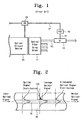
FIG. 1 , atap coupler 15 for dividing an optical signal at a constant ratio is coupled to eachoptical fiber 13 from anoptical circuit device 10 with a horizontal waveguide integrated therein and an opticalfiber array block 11. As a light receiving element, amonitor photodiode 19 for detecting the intensity of an optical signal is optically coupled to one end of an optical line that branches by abranch coupler 15. The optical signal detected from thephotodiode 19 generates photocurrent having a functional relation to the intensity thereof, and is inputted to acontrol module 23 via anelectric wire 21. The optical signal processed in thecontrol module 23 is feedbacked to a controller of theoptical circuit device 10 of a previous stage when an optical signal already passed, controlling an attenuation rate of the optical signal. - Unfortunately, the above-described approach encounters a problem. The problem is to necessarily to install a branch coupler and a light receiving element in each channel, and to install a control module to be transmitted to an optical circuit device of a previous stage by processing an electrical signal of the light receiving element. Further, the space for a photo wire connecting them is needed. Therefore, this approach requires a number of parts used for measuring the intensity of the optical signal throughout a number of channels. Since each of the parts has a great volume and their connection structure is very complicated, there is difficulty in integrating devices, used in this approach, in a small-sized module. In conclusion, the process for uniformly controlling the intensity of an optical signal leads to increase in the total volume of an optical communication apparatus as well as complication of a structure and a fabricating process.
-
JP 2001 183552 -
US 5,892,857 discloses an electro-optic modulator in the form of a compound waveguide device having a channel waveguide in optical proximity to an elongate waveguide propagating an optical signal therein. The channel waveguide is formed from an electro-optically active material, and modulation of the optical signal propagating in the elongate waveguide is effected using the evanescent coupling effect between the two waveguides. - In order to overcome the foregoing disadvantages, the present
- invention provides an optical fiber array block where a detection module for measuring the intensity of an optical signal to an optical waveguide is integrated and miniaturized in an optical circuit device to facilitate a process for forming an associated device and realize a mass production by way of an automated work.
- According to the present invention there is provided an optical fiber array block, the block comprising:
- an optical waveguide including a plurality of optical fibers (101), each optical fiber being settled in one of a plurality of grooves (105) formed on a board (100) and each optical fibre including a core (31), a clad layer (33) having a first clad thickness and comprising one or more leakage window each formed in a portion of the clad layer having a thickness that is less then the first clad thickness;
- one or more optical devices (121) for detecting optical signal output from the one or more leakage windows each of the one or more optical devices (121) corresponding to a predetermined leakage window; and
- an intermediate panel (110) interposed between the one or more optical devices and the one or more leakage windows (104),
- The optical fiber array block according to the invention therefore comprises an optical waveguide including a space for optical fibers on a board includes leakage windows installed on the optical waveguide, and optical devices arranged to correspond to the leakage window.
- The optical waveguide is composed of optical fibers each including a core and a clad layer that are around the leakage window made partially from the clad layer. The optical device is one of a photodiode and a kind of photo receiving device. The optical waveguide is made of an optical fiber array composed of a plurality of optical fibers each being settled in each of grooves formed on the board. The leakage windows are parallel to the optical fiber array along a direction crossing the grooves. The optical devices are arranged along the direction to be spaced with same intervals to each other together with the leakage windows.
- The optical fiber array block further comprises an intermediate panel interposed between the substrate and the board, electric terminals connectable to the optical devices on the substrate, guiding holes penetrating the intermediate panel to lead optical signals emitted from the leakage windows to the optical devices, junction pads connected to the electric terminals, electric wires led from the junction pads, and electrode pads positioned at ends of the electric wires.
- Also the optical fiber array block further includes an intermediate panel installed on the substrate to electrically connect the substrate to the board, electric terminals connectable to the optical devices on the substrate, junction
- pads arranged on a bottom side of the intermediate panel and connected to the electric terminals, electric wires led from the junction pads, conductive patterns contacting with the electrode pads when the board joins to the intermediate panel, substrate wires led from the conductive patterns, and wire-bonded electrode pads arranged on a edge surface of the board. The edge surface is out of covering by the intermediate panel.
- Also the optical fiber array block further includes fosses formed at boundaries of the block cap to stop spread of glue.
-
-
FIG. 1 is a schematic diagram partially showing the structure of a conventional optical circuit for measuring the intensity of an optical signal at each optical waveguide channel. -
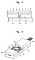
FIG. 2 is a cross-sectional view showing one section of an optical fiber in which an optical signal leakage window is formed according to the present invention. -
FIG. 3 is a state diagram for explaining the state that the optical signal leakage window according to the invention is formed by an ion implanting process. -
FIG. 4 is a perspective view showing the appearance of an optical fiber array block according to a first embodiment of the invention. -
FIG. 5 is an exploded perspective view for explaining a detailed structure of the optical array block shown inFIG. 4 and a method of forming the same. -
FIG. 6 is a cross-sectional view of the optical fiber array block shown inFIG. 4 , taken along an optical fiber. -
FIG. 7 is an exploded perspective view showing an optical fiber array block substrate on which an electrode pad for wire bonding is formed, according to a second embodiment of the invention. -
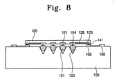
FIG. 8 is a cross-sectional view of an optical fiber array block, vertically taken along the optical fiber forming direction at a position where an optical signal leakage window is formed according to a third embodiment of the invention. -
FIG. 9 is an exploded perspective view showing a fourth embodiment of the invention. -
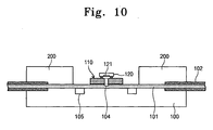
FIG. 10 is a cross-sectional view of a fifth embodiment of the invention. - A principle of the present invention is explained in detail with reference to
FIG. 2 , which shows an optical fiber having an optical signal leakage window. - Referring to
FIG. 2 , an optical fiber includes acore 31 into which an optical signal passing the optical fiber is almost concentrated, and aclad layer 33 surrounding a periphery of thecore 31. Because an optical signal transmitted through thecore 31 is totally reflected at a boundary of theclad layer 33, it is almost concentrated into thecore 31. An optical signal passing a specific spot at a specific time is concentrated into thecore 31, and a distribution state of the optical signal is exhibited by means of the Gaussian distribution centered at thecore 31. Theclad layer 33 is partially removed at an opticalsignal leakage window 104, exposing an optical signal passing thewindow 104 to the exterior of an optical fiber. The total optical signal, which passed the opticalsignal leakage window 104, is realigned to reestablish the Gaussian distribution. Accordingly, a peak value of the realigned distribution is reduced as compared to a peak value of the Gaussian distribution before passing the opticalsignal leakage window 104. - An optical leakage window may be formed by implanting impurities into the
clad layer 33 using a mask exposing an optical signal portion where theleakage window 104 is to be formed, as shown inFIG. 3 . In this case, the impurity-implanted window is connected to thecore 31 and a refractive index of theleakage window 104 becomes equal to that of thecore 31. Thus, the total reflection of the optical signal is suppressed at theleakage window 104 to leak an optical signal through theleakage window 104. - If a light electric element such as a photodiode is installed at a position opposite to a leakage window, it detects a small optical signal leaked through the leakage window to measure the intensity of an optical signal passing the whole optical fiber. Based on the measurement, optical signal intensities in channels can be compared and controlled.
- Meanwhile, if a light element such as a diode is installed thereat, a light produced from an optical device may travel into the optical fiber. By adding or subtracting a pattern of the optical signal in a transmitting part and a receiving part, a security communication may be achieved. In view of this and other advantages, the present invention is suggested.
- If an optical fiber array includes a plurality of optical fibers, it is preferable to form optical signal leakage windows having the same size, shape, and refraction characteristic at the optical fibers respectively. It is also preferable that equivalent are the distance and relative position of an optical signal leakage window and a corresponding photodiode as well as the intermediary space of a medium. In conclusion, if optical signal intensities are compared with one another, increase or decrease in optical signal intensity of each channel and other handlings may be carried out through feedback by comparing the relative intensities of optical signals passing optical fibers constituting an array.
- An appearance of an optical fiber array block according to a first embodiment of the invention is illustrated in
FIG. 4 . - Referring to
FIG. 4 , a plurality of V-shaped grooves are horizontally formed on ablock board 100. An uncoatedoptical fiber 101 is placed in the respective V-shaped grooves. Ablock cap 200 corresponding to theblock board 100 is disposed on the V-shaped grooves. Theblock cap 200 is cut a predetermined width along the horizontal direction of the groove. Glue-spread-preventinggrooves 105 are formed on the block board adjacent to opposite peripheries of a region where theblock cap 200 is cut. Between thegrooves 105, theblock board 100 and the optical fiber are covered with amedium panel 110. Anoptical device board 120 is disposed in the center of a top surface of themedium panel 110.Electric wires 118 andjunction pads 117 are formed on the top surface of themedium panel 110. Thejunction pads 117 are disposed at ends of the correspondingelectric wires 118, respectively. -
FIG. 5 is a perspective exploded view for explaining a detailed structure of an optical fiber array block as shown inFIG. 4 and a method of forming the same. - Referring to
FIG. 5 , theblock board 100 is similar to a rectangular parallelepiped block. Theblock board 100 is made of silicon, glass, pyrex and so forth. A plurality of V-shapedgrooves 103 are formed in the center of a top surface of theblock board 100 to be perpendicular to a long side of theblock board 100. Twogrooves 105 for glue spread prevention are formed on theblock board 100 to be perpendicular to the V-shapedgrooves 103. A section having four edges is defined between the twogrooves 105. An alignment mark is formed at the respective edges, and a linear mark representing a position of the opticalsignal leakage window 104 is formed parallel to the twogrooves 105. - Each of the
optical fibers 101 constituting an optical fiber array is placed without aprotection cover 102. In the optical fiber array, an opticalsignal leakage window 104 is formed over theoptical fiber 101 without theprotection cover 102 at a position where thelinear mark 107 is formed. Theleakage window 104 may be formed by partially cutting theoptical fiber 101 or implanting impurities. Accordingly, theparallel leakage windows 104 are disposed at a position of thelinear mark 107 throughout the optical fiber array. - On an
intermediary panel 110, guidingholes 111 are formed corresponding to each of the opticalsignal leakage windows 104 formed in the optical fiber array. The guiding holes 111 are attached to theblock board 100. Therefore, the guidingholes 111 are also disposed parallel to thelinear marks 107. Two flipchip junction pads 113 are formed on theintermediary panel 110 so as to drive aphotodiode 121, respectively. An electric wire 181 leads to therespective junction pads 113. One end of the electric wire 181 is coupled to a wirebonding electrode pad 117 formed parallel to opposite peripheries of theintermediary panel 110. - An
optical device substrate 120 is aligned and attached to a part where the guidingholes 111 are formed. A plurality ofphotodiodes 121 are formed below theoptical device substrate 120 so as to cover the guiding holes 111 formed on theintermediary panel 110. In a case where thephotodiode 121 are distant apart from the opticalsignal leakage window 104 and the optical fibers are closely adjacent to each other, without the guidinghole 111, the intensity of an optical signal traveling into thephotodiode 121 becomes low. Further an optical signal, which is leaked at the opticalsignal leakage window 104 formed in the adjacentoptical fiber 101, may affect thephotodiode 121 corresponding to another opticalsignal leakage window 104. In order to prevent the above disadvantage, the guidinghole 111 serves to induce most optical signals, which are leaked from the opticalsignal leakage window 104, to correspondingphotodiodes 121. - Each of the
photodiodes 121 is installed to expose twoelectric connection terminals 123 at both sides thereof. Therefore, theintermediary panel 110 may be attached to anelectric connection terminal 120 of thesubstrate 120 by a flip chip junction technique to solder aconnection pad 113. After theintermediary panel 110 and thesubstrate 120 are attached to make an optical device panel, the guidinghole 111 is covered by a light receiving window of thecorresponding photodiode 121. Alignment marks 125 and 115 are formed on a lower side of thesubstrate 120 and a corresponding upper side of theintermediary panel 110, respectively. - On the upper side of the
block board 100, the optical device panel is aligned and attached to an area defined between the twogrooves 105 by glue. In order to align the optical device panel, alignment marks 119 matching analignment mark 109 formed on the defined area are previously formed at corners of theintermediary panel 110. Ablock cap 200 is attached to the defined area and an external upper side of the twogrooves 105 by glue. The twogrooves 105 prevent the glue used to attach theblock cap 200 from spreading out the defined area and capping the opticalsignal leakage window 104. - With reference to
FIG. 6 , there is illustrated interrelationship of thephotodiode 121 of theoptical device substrate 120, the opticalsignal guiding hole 111 of theintermediary panel 110, and the opticalsignal leakage window 104. Using a manner of controlling a refractive index to enhance a sensing efficiency, a liquid phase material or a solidified material may fill a space between thephotodiode 121 and theintermediary panel 110, the opticalsignal induction pipe 111, an the opticalsignal leakage window 104. Theintermediary panel 110 and theoptical device substrate 120 are attached to each other by means of a flip chip junction technique using asolder 143. - A second embodiment of the present invention will now be described with reference to
FIG. 7 . - The second embodiment is identical to the first embodiment, except that an
electric wire 118 is connected to a flipchip junction pad 114 through a viacontact 115. Theelectric wire 118 extends from a flipchip junction pad 113 formed on anintermediary panel 110. When theintermediary panel 110 is aligned and attached to ablock board 100,conductive patterns 106 are formed such that theintermediary panel 110 is connected to the flipchip junction pad 114. Each of theconductive patterns 106 is connected to anelectrode pad 117 for wire bonding by an electric wire extending to an exterior. Thus, while the wire is connected to theelectrode pad 117 formed OD theintermediary panel 110 in the first embodiment, the wire is connected to theelectrode pad 108 formed on theblock board 100 in the second embodiment. - In order to adjust a height of the wire bonding, a height adjusting unit may be installed at a portion where the
electrode pad 108 for wire bonding is formed. In this case, there is a steep difference between the height adjusting unit and theblock board 100. - A third embodiment of the present invention will now be described with reference to
FIG. 8 . - Referring to
FIG. 8 , an intermediary panel is not used in the third embodiment. Aphotodiode 121 is formed below anoptical device substrate 120. Anelectric wire 128 and a flipchip junction pad 123 are formed directly beneath theoptical device substrate 120, while being formed at the intermediary panel in the prior art. Similar to the second embodiment, when theoptical device substrate 120 is aligned and attached to a block board of an optical fiber array block,conductive patterns 106 are formed to connect to the flipchip junction pad 123. Each of theconductive patterns 106 is connected to anelectrode pad 108 for wire bonding by an electric wire extending to an exterior. - A fourth embodiment of the present invention will now be described with reference to
FIG. 9 . Unlike the second embodiment, an optical device substrate is interposed between an intermediary panel and a block board without an optical signal guiding hole and a via contact. - Referring to
FIG. 9 , aheight adjusting lid 121 is formed at a flip chip junction pad, so that a space is formed between anintermediary panel 110 and ablock board 100. Anoptical device substrate 120 can be contained in the space. Aphotodiode 121 is formed on a lower side of theoptical device substrate 120 by means of a die bonding technique. Aconnection terminal 123 is formed on an upper side of theoptical device substrate 120 through a contact 222. Theconnection terminal 123 and theheight adjusting lid 121 are aligned and attached to each other based on a flip chip manner. In this case, thephotodiode 121 are opposite to an opticalsignal leakage window 104. The flip chip junction pad is attached to aconductive pad 106 of theblock board 100 through theheight adjusting lid 121 based on the flip chip manner. - A fifth embodiment of the present invention will now be described with reference to
Fig. 10 . While the first to fifth embodiments relate to an optical fiber array block that is used in an optical module in the early stage, the fifth embodiment relates to an optical fiber array block that may be used in the exterior of an optical fiber module without a leakage window and an optical device connected thereto. - Referring to
FIG. 10 , an opticalfiber protection cover 102 is removed at several portions of anoptical fiber 101 for forming a separate waveguide in an existing optical circuit. Glue-spread-preventinggrooves 105 are preferably formed at a boundary of ablock board 100 corresponding to a portion where ablock cap 200 is removed. Anoptical fiber 101 is fixed to a V-shaped groove or in position of theblock board 100. In this case, a portion of the optical fiber with the removedprevention cover 102 is located at theblock board 100 corresponding to the portion where theblock cap 200 is removed. By means of a cutting or ion-implanting technique, an opticalsignal leakage window 104 is formed at a clad layer of one or more optical fibers that are horizontally arranged. An optical device panel, which comprises a separate optical device or an optical device panel or anoptical device substrate 120 and anintermediary panel 110, is aligned and attached to theblock board 100 such that aphotodiode 121 covers an opticalsignal leakage window 104 at a position corresponding to theleakage window 104. Each electrode of the optical device may be connected to an eternal electric connection pad that may be formed at an optical device panel or a block board. The electric connection may be done by means of a junction solder, a conductive line, a contact, and so forth. Using glue, theblock cap 200 covers theblock board 100. - Although not shown in the figures, a part corresponding to the
control module 23 shown inFIG. 1 may be monolithically formed on an upper side of an optical device substrate, an intermediary panel or a block board. As a result, a photodiode direct optical fiber array block having an automatic control function can be fabricated. - According to the present invention, in a case where an optical fiber array type optical signal device used in a wavelength multiple division system detects the intensity of an optical signal, a leakage window is formed at a part of an optical fiber fixed to an optical fiber array block without a separate device such as a branch coupling element. The intensity of the optical signal is correctly detected and measured in the optical signal device. Therefore, it is possible to fabricate an integrated and miniaturized detection module for measuring the intensity of an optical signal of an optical waveguide. Further, it is possible to reduce the installing spaces of many optical devices in receive and transmit terminals of an optical circuit and to facilitate their installment.
Claims (19)
- An optical fiber array block, the block comprising:an optical waveguide including a plurality of optical fibers (101), each optical fiber being settled in one of a plurality of grooves (105) formed on a board (100) and each optical fibre including a core (31), a clad layer (33) having a first clad thickness and comprising one or more leakage window each formed in a portion of the clad layer having a thickness that is less then the first clad thickness;one or more optical devices (121) for detecting optical signal output from the one or more leakage windows each of the one or more optical devices (121) corresponding to a predetermined leakage window; andan intermediate panel (110) interposed between the one or more optical devices and the one or more leakage windows (104),characterised in that the intermediate panel has one or more guiding holes (111) penetrating the intermediate panel (110) each of which holes defines an optical waveguide to lead optical signals emitted from a leakage window to a corresponding optical device.
- An optical fiber array block, according to claim 1, wherein each of the leakage windows (104) is formed by partially implanting ions into the clad layer surrounding a periphery of the core along the optical waveguide, using a mask, and in that each of the leakage windows has a refractive index substantially equal to that of the core.
- The block of claim 1 or claim 2, wherein the optical devices (121) are one of a photodiode and a photo receiving device.
- The block of claim 1 or claim 2, wherein the leakage windows (104) are spaced apart from one another by an interval and are arranged in a direction parallel to the axis of the optical fibre (101),
and wherein the optical devices (121) are arranged in the same direction as that in which the leakage windows (104) are arranged, the optical devices (121) being spaced apart from one another by same interval as that of the leakage windows (104). - The block of claim 1 or claim 2, wherein the optical devices (121) are formed on a substrate.
- The block of claim 5, wherein the intermediate panel (110) comprises:a plurality of junction pads (113) connected to a plurality of electric terminals (123);a plurality of electric wires (118) led from the junction pads (113); anda plurality of electrode pads (117) positioned at ends of the electric wires (118),wherein electric terminals (123) connectable to the optical devices (121) are formed on the substrate (120).
- The block of claim 5, wherein alignment marks (125, 115) are inscribed at locations where the substrate (120) and the intermediate panel (110) are opposite to and face each other.
- The block of claim 1 or claim 2, wherein alignment marks (119, 109) are inscribed at locations where the intermediate panel (110) and the board (100) are opposite to and face each other.
- The block of claim 1 or claim 2, wherein the one or more guiding holes (111) are filled with a material available for adjusting a refractive index of light.
- The block of claim 6, wherein the substrate (120) adheres to the intermediate panel (110) by means of a flip chip joining between the electric terminals (123) and the junction pads (113).
- The block of claim 6, wherein the electric terminals (123) are formed on a top side of the intermediate panel (110), being connectably wire-bonded to external electric wires.
- The block of claim 6, wherein the junction pads (113), while formed on a bottom side of the intermediate panel (110), are connected to conductive patterns (106) through the electric wires by way of via contact holes (112) when the intermediate panel (110) joins to the board (100), the conductive patterns (106) being electrically connected to wire bonded etectrode pads (108) arranged on an edge surface of the board (100), the edge surface being put of covering by the intermediate panel (110).
- The block of claim 12, wherein conductive patterns (106) are contacted with the junction pads (114) by means of a flip chip joining using a solder ball, so that the board (100) adheres to the intermediate panel (110).
- The block of claim 5, wherein the substrate includes a module in which the optical devices (121) are associated with processing circuits thereof.
- The block of claim 1 or claim 2, further comprising a block cap (200) shielding the optical waveguide while opening regions of the leakage windows (104).
- The block of claim 15, further comprising fosses (105) formed at boundaries of the block cap (200) to stop the spread of glue.
- The block of claim 1 or claim 2, wherein the optical waveguide is composed of optical fibers (101), one end of each of the optical fibres (101) being cut away while the other end of each fibre is coupled to an optical circuit.
- The block of claim 1 or claim 2, wherein the optical waveguide is composed of optical fibers (101), both ends of each optical fibres (101) being coupled to an optical circuit.
- The block of claim 1 or claim 2, further comprising a control module for processing signals generated from the optical devices (121).
Applications Claiming Priority (3)
| Application Number | Priority Date | Filing Date | Title |
|---|---|---|---|
| KR10-2001-0069428A KR100416688B1 (en) | 2001-11-08 | 2001-11-08 | Optical fiber block integrated with photo device |
| KR2001069428 | 2001-11-08 | ||
| PCT/KR2002/002063 WO2003040795A1 (en) | 2001-11-08 | 2002-11-06 | Optical fiber array block embedding optical device therein |
Publications (3)
| Publication Number | Publication Date |
|---|---|
| EP1442328A1 EP1442328A1 (en) | 2004-08-04 |
| EP1442328A4 EP1442328A4 (en) | 2005-11-16 |
| EP1442328B1 true EP1442328B1 (en) | 2008-09-10 |
Family
ID=19715820
Family Applications (1)
| Application Number | Title | Priority Date | Filing Date |
|---|---|---|---|
| EP02790959A Expired - Lifetime EP1442328B1 (en) | 2001-11-08 | 2002-11-06 | Optical fiber array block embedding optical device therein |
Country Status (9)
| Country | Link |
|---|---|
| US (1) | US7010192B2 (en) |
| EP (1) | EP1442328B1 (en) |
| JP (1) | JP4050701B2 (en) |
| KR (1) | KR100416688B1 (en) |
| CN (1) | CN1582405A (en) |
| AT (1) | ATE408164T1 (en) |
| DE (1) | DE60228868D1 (en) |
| TW (1) | TW557380B (en) |
| WO (1) | WO2003040795A1 (en) |
Families Citing this family (19)
| Publication number | Priority date | Publication date | Assignee | Title |
|---|---|---|---|---|
| KR100576152B1 (en) | 2004-01-16 | 2006-05-03 | 주식회사 골드텔 | Optical signal detector |
| KR100616549B1 (en) * | 2004-01-16 | 2006-08-28 | 주식회사 골드텔 | Optical cable for optical signal detection and method of manufacturing same |
| KR100651221B1 (en) | 2005-04-27 | 2006-11-30 | 주식회사 골드텔 | Optical signal detector |
| KR100651238B1 (en) | 2005-04-27 | 2006-11-30 | 주식회사 골드텔 | Optical signal detector |
| TWI368768B (en) * | 2007-12-28 | 2012-07-21 | Ind Tech Res Inst | Optical intermediary component and optical daughter card module |
| KR101023136B1 (en) * | 2009-02-18 | 2011-03-18 | 한국광기술원 | Optical module device with optical fiber network monitoring device |
| US8280203B2 (en) * | 2009-07-07 | 2012-10-02 | Avago Technologies Fiber Ip (Singapore) Pte. Ltd | Parallel optical communications device having weldable inserts |
| JP2013140259A (en) * | 2012-01-05 | 2013-07-18 | Ntt Electornics Corp | Receiving package for flat plate arrangement, optical module, and manufacturing method of receiving package for flat plate arrangement |
| WO2013157761A1 (en) * | 2012-04-20 | 2013-10-24 | Bae Byoung-Young | Apparatus and method for processing an optical fiber |
| CN108181687A (en) * | 2012-11-29 | 2018-06-19 | 深圳迈辽技术转移中心有限公司 | A kind of opto-electronic conversion method of photoelectric conversion device |
| US9178618B2 (en) | 2013-10-22 | 2015-11-03 | Globalfoundries Inc. | Preassembled optoelectronic interconnect structure |
| CN103777280B (en) | 2014-01-27 | 2016-06-15 | 华进半导体封装先导技术研发中心有限公司 | A kind of optical fiber assembly with angle of inclination and assembly method thereof |
| KR20160071810A (en) * | 2014-12-12 | 2016-06-22 | (주)파이버프로 | Polarization maintain fiber array block and manufacturing method of the same |
| CN105572815B (en) * | 2015-12-21 | 2018-02-23 | 华进半导体封装先导技术研发中心有限公司 | Active optics pinboard and optical interconnection module |
| EP3400486B1 (en) * | 2016-01-04 | 2023-06-07 | Infinera Corporation | Photonic integrated circuit package |
| CN105911644B (en) * | 2016-06-01 | 2019-06-04 | 中国电子科技集团公司第四十一研究所 | A kind of optical fiber collimation device and its assembly method |
| JP6933794B2 (en) * | 2016-12-01 | 2021-09-08 | 富士通株式会社 | Optical module and manufacturing method of optical module |
| WO2020184801A1 (en) * | 2019-03-13 | 2020-09-17 | 송수복 | Shoe upper with illuminating logo and shoe including same |
| CN119224936A (en) * | 2023-06-30 | 2024-12-31 | 华为技术有限公司 | Optical fiber connector, optical splitter |
Family Cites Families (34)
| Publication number | Priority date | Publication date | Assignee | Title |
|---|---|---|---|---|
| US3777149A (en) * | 1972-07-17 | 1973-12-04 | Bell Telephone Labor Inc | Signal detection and delay equalization in optical fiber transmission systems |
| DE2553685C2 (en) * | 1975-11-28 | 1985-05-09 | Siemens AG, 1000 Berlin und 8000 München | Method of manufacturing an optical directional coupler |
| US4076375A (en) * | 1975-12-24 | 1978-02-28 | Bell Telephone Laboratories, Incorporated | Directional optical waveguide coupler and power tap arrangement |
| US4081672A (en) * | 1976-10-04 | 1978-03-28 | The United States Of America As Represented By The Secretary Of The Navy | Low-loss signal coupler for optical communications and integrated optics |
| US4558920A (en) * | 1981-11-19 | 1985-12-17 | Board Of Trustees Of The Leland Stanford Junior University | Tapped optical fiber delay line |
| US4514057A (en) * | 1981-12-23 | 1985-04-30 | General Dynamics Pomona Division | Fiber optic coupler array and fabrication method |
| WO1984002005A1 (en) * | 1982-11-12 | 1984-05-24 | Univ Leland Stanford Junior | Fiber optic switch and discretely variable delay line |
| US4549782A (en) * | 1983-06-06 | 1985-10-29 | At&T Bell Laboratories | Active optical fiber tap |
| GB2168165B (en) * | 1984-12-10 | 1988-08-10 | Electronic Components Ltd | Tap for data transmission system |
| US4900118A (en) * | 1987-05-22 | 1990-02-13 | Furukawa Electric Co., Ltd. | Multiple-fiber optical component and method for manufacturing of the same |
| US5037172A (en) * | 1989-03-22 | 1991-08-06 | Teledyne Industry, Inc. | Fiber optic device with a reflective notch coupler |
| US5042896A (en) * | 1990-08-30 | 1991-08-27 | The Charles Stark Draper Laboratory, Inc. | Polarization device |
| US5101090A (en) * | 1990-11-19 | 1992-03-31 | At&T Bell Laboratories | Methods and apparatus for making optical fiber couplers |
| DE4114629A1 (en) * | 1991-04-30 | 1992-11-05 | Siemens Ag | LIGHT WAVE GUIDE WITH A COUPLING AREA |
| US5170448A (en) * | 1992-01-06 | 1992-12-08 | Motorola, Inc. | Optical waveguide apparatus and method for partially collecting light |
| JPH05297331A (en) | 1992-04-17 | 1993-11-12 | Nec Corp | Optical variable attenuating device |
| US5757989A (en) * | 1992-09-10 | 1998-05-26 | Fujitsu Limited | Optical circuit system capable of producing optical signal having a small fluctuation and components of same |
| US5659643A (en) * | 1995-01-23 | 1997-08-19 | Minnesota Mining And Manufacturing Company | Notched fiber array illumination device |
| JP2800715B2 (en) * | 1995-05-12 | 1998-09-21 | 日本電気株式会社 | Optical fiber amplifier |
| US5903685A (en) * | 1995-11-29 | 1999-05-11 | British Telecommunications Public Limited Company | Sensor arrangement |
| JPH09311253A (en) * | 1996-05-20 | 1997-12-02 | Fujitsu Ltd | Optical coupling structure and manufacturing method thereof |
| US5854864A (en) * | 1996-07-16 | 1998-12-29 | The Regents Of The University Of California | In-line polymeric construct for modulators, filters, switches and other electro-optic devices |
| KR100211039B1 (en) * | 1996-12-20 | 1999-07-15 | 이계철 | Optical switch-optical fiber optical coupler |
| US5892857A (en) | 1997-01-21 | 1999-04-06 | Molecular Optoelectronics Corporation | Electro-optic compound waveguide intensity modular and method using same |
| JP3495578B2 (en) | 1997-10-03 | 2004-02-09 | 古河電気工業株式会社 | Optical fiber amplifier |
| US5966493A (en) * | 1998-02-20 | 1999-10-12 | Molecular Optoelectronics Corporation | Fiber optic attenuators and attenuation systems |
| EP1008876A3 (en) * | 1998-12-11 | 2003-03-26 | Litton Systems, Inc. | Optical fiber tap and method of tapping an optical signal from an optical cable |
| US6246819B1 (en) * | 1998-12-11 | 2001-06-12 | Prc Inc. | Fiber optic cladding displacement connector |
| US6490388B1 (en) * | 1999-03-08 | 2002-12-03 | Optigain, Inc. | Side-pumped fiber laser |
| JP2001183552A (en) * | 1999-12-22 | 2001-07-06 | Yazaki Corp | Method and apparatus for detecting light in optical fiber |
| US6456766B1 (en) * | 2000-02-01 | 2002-09-24 | Cornell Research Foundation Inc. | Optoelectronic packaging |
| US6788865B2 (en) * | 2000-03-03 | 2004-09-07 | Nippon Telegraph And Telephone Corporation | Polarization maintaining optical fiber with improved polarization maintaining property |
| US6490391B1 (en) * | 2000-07-12 | 2002-12-03 | Oluma, Inc. | Devices based on fibers engaged to substrates with grooves |
| US6744948B1 (en) * | 2001-06-20 | 2004-06-01 | Oluma, Inc. | Fiber tap monitor based on evanescent coupling |
-
2001
- 2001-11-08 KR KR10-2001-0069428A patent/KR100416688B1/en not_active Expired - Lifetime
-
2002
- 2002-07-19 TW TW091116092A patent/TW557380B/en not_active IP Right Cessation
- 2002-11-06 US US10/493,640 patent/US7010192B2/en not_active Expired - Lifetime
- 2002-11-06 AT AT02790959T patent/ATE408164T1/en not_active IP Right Cessation
- 2002-11-06 DE DE60228868T patent/DE60228868D1/en not_active Expired - Lifetime
- 2002-11-06 EP EP02790959A patent/EP1442328B1/en not_active Expired - Lifetime
- 2002-11-06 CN CNA028218418A patent/CN1582405A/en active Pending
- 2002-11-06 JP JP2003542375A patent/JP4050701B2/en not_active Expired - Lifetime
- 2002-11-06 WO PCT/KR2002/002063 patent/WO2003040795A1/en not_active Ceased
Also Published As
| Publication number | Publication date |
|---|---|
| EP1442328A1 (en) | 2004-08-04 |
| TW557380B (en) | 2003-10-11 |
| KR100416688B1 (en) | 2004-01-31 |
| US20040264865A1 (en) | 2004-12-30 |
| KR20030038023A (en) | 2003-05-16 |
| US7010192B2 (en) | 2006-03-07 |
| JP4050701B2 (en) | 2008-02-20 |
| ATE408164T1 (en) | 2008-09-15 |
| CN1582405A (en) | 2005-02-16 |
| JP2005508519A (en) | 2005-03-31 |
| EP1442328A4 (en) | 2005-11-16 |
| DE60228868D1 (en) | 2008-10-23 |
| WO2003040795A1 (en) | 2003-05-15 |
Similar Documents
| Publication | Publication Date | Title |
|---|---|---|
| US7010192B2 (en) | Optical fiber array block embedding optical device therein | |
| US6374021B1 (en) | Light transmitting/receiving module | |
| EP1028339B1 (en) | Light transmitting/receiving module | |
| US6241399B1 (en) | Ferrule assembly and optical module | |
| JP3750649B2 (en) | Optical communication device | |
| US20050105848A1 (en) | Optical waveguide modulator with output light monitor | |
| US6408121B1 (en) | Optical communication module | |
| US20220035100A1 (en) | Optical Circuit and Optical Connection Structure | |
| US7203390B2 (en) | Planar lightwave circuit package | |
| CA2354457C (en) | An optical transmitter-receiver module | |
| CN100376909C (en) | Optical element, optical transceiver and other optical device using the optical element | |
| US7394952B1 (en) | Optical transmission device and optical module | |
| KR101216732B1 (en) | Optical power monitoring module using the thin flexible pcb, and the manufacturing method | |
| KR101220303B1 (en) | Optical power monitoring module | |
| EP1115012B1 (en) | Waveguide with tap recess for optical monitoring in photonic devices | |
| JP2003004991A (en) | Optical transmitting / receiving module and manufacturing method thereof | |
| JP2008040029A (en) | OPTICAL ELEMENT FOR MONITORING AND MANUFACTURING METHOD THEREOF | |
| JP2006259769A (en) | Optical waveguide device, manufacturing method thereof, and optical communication device | |
| KR20130055818A (en) | Method for manufacturing hybrid integration of monitor photodiode on plc platform | |
| JPH0372306A (en) | Waveguide type wavelength multiplex transmission/ reception module | |
| JPH10308528A (en) | Optical semiconductor module |
Legal Events
| Date | Code | Title | Description |
|---|---|---|---|
| PUAI | Public reference made under article 153(3) epc to a published international application that has entered the european phase |
Free format text: ORIGINAL CODE: 0009012 |
|
| 17P | Request for examination filed |
Effective date: 20040430 |
|
| AK | Designated contracting states |
Kind code of ref document: A1 Designated state(s): AT BE BG CH CY CZ DE DK EE ES FI FR GB GR IE IT LI LU MC NL PT SE SK TR |
|
| RIN1 | Information on inventor provided before grant (corrected) |
Inventor name: CHOI, JAE-SHIK Inventor name: CHUNG, KI-WOO Inventor name: JOO, GWAN-CHONG Inventor name: KIM, DO-HOON |
|
| A4 | Supplementary search report drawn up and despatched |
Effective date: 20050930 |
|
| 17Q | First examination report despatched |
Effective date: 20060703 |
|
| GRAP | Despatch of communication of intention to grant a patent |
Free format text: ORIGINAL CODE: EPIDOSNIGR1 |
|
| GRAS | Grant fee paid |
Free format text: ORIGINAL CODE: EPIDOSNIGR3 |
|
| GRAA | (expected) grant |
Free format text: ORIGINAL CODE: 0009210 |
|
| AK | Designated contracting states |
Kind code of ref document: B1 Designated state(s): AT BE BG CH CY CZ DE DK EE ES FI FR GB GR IE IT LI LU MC NL PT SE SK TR |
|
| REG | Reference to a national code |
Ref country code: GB Ref legal event code: FG4D |
|
| REG | Reference to a national code |
Ref country code: CH Ref legal event code: EP |
|
| REG | Reference to a national code |
Ref country code: IE Ref legal event code: FG4D |
|
| REF | Corresponds to: |
Ref document number: 60228868 Country of ref document: DE Date of ref document: 20081023 Kind code of ref document: P |
|
| PG25 | Lapsed in a contracting state [announced via postgrant information from national office to epo] |
Ref country code: AT Free format text: LAPSE BECAUSE OF FAILURE TO SUBMIT A TRANSLATION OF THE DESCRIPTION OR TO PAY THE FEE WITHIN THE PRESCRIBED TIME-LIMIT Effective date: 20080910 Ref country code: FI Free format text: LAPSE BECAUSE OF FAILURE TO SUBMIT A TRANSLATION OF THE DESCRIPTION OR TO PAY THE FEE WITHIN THE PRESCRIBED TIME-LIMIT Effective date: 20080910 |
|
| NLV1 | Nl: lapsed or annulled due to failure to fulfill the requirements of art. 29p and 29m of the patents act | ||
| PG25 | Lapsed in a contracting state [announced via postgrant information from national office to epo] |
Ref country code: BE Free format text: LAPSE BECAUSE OF FAILURE TO SUBMIT A TRANSLATION OF THE DESCRIPTION OR TO PAY THE FEE WITHIN THE PRESCRIBED TIME-LIMIT Effective date: 20080910 |
|
| PG25 | Lapsed in a contracting state [announced via postgrant information from national office to epo] |
Ref country code: ES Free format text: LAPSE BECAUSE OF FAILURE TO SUBMIT A TRANSLATION OF THE DESCRIPTION OR TO PAY THE FEE WITHIN THE PRESCRIBED TIME-LIMIT Effective date: 20081221 Ref country code: BG Free format text: LAPSE BECAUSE OF FAILURE TO SUBMIT A TRANSLATION OF THE DESCRIPTION OR TO PAY THE FEE WITHIN THE PRESCRIBED TIME-LIMIT Effective date: 20081210 |
|
| PG25 | Lapsed in a contracting state [announced via postgrant information from national office to epo] |
Ref country code: CZ Free format text: LAPSE BECAUSE OF FAILURE TO SUBMIT A TRANSLATION OF THE DESCRIPTION OR TO PAY THE FEE WITHIN THE PRESCRIBED TIME-LIMIT Effective date: 20080910 Ref country code: NL Free format text: LAPSE BECAUSE OF FAILURE TO SUBMIT A TRANSLATION OF THE DESCRIPTION OR TO PAY THE FEE WITHIN THE PRESCRIBED TIME-LIMIT Effective date: 20080910 Ref country code: SK Free format text: LAPSE BECAUSE OF FAILURE TO SUBMIT A TRANSLATION OF THE DESCRIPTION OR TO PAY THE FEE WITHIN THE PRESCRIBED TIME-LIMIT Effective date: 20080910 Ref country code: PT Free format text: LAPSE BECAUSE OF FAILURE TO SUBMIT A TRANSLATION OF THE DESCRIPTION OR TO PAY THE FEE WITHIN THE PRESCRIBED TIME-LIMIT Effective date: 20090210 |
|
| PG25 | Lapsed in a contracting state [announced via postgrant information from national office to epo] |
Ref country code: MC Free format text: LAPSE BECAUSE OF NON-PAYMENT OF DUE FEES Effective date: 20081130 |
|
| REG | Reference to a national code |
Ref country code: CH Ref legal event code: PL |
|
| PLBE | No opposition filed within time limit |
Free format text: ORIGINAL CODE: 0009261 |
|
| STAA | Information on the status of an ep patent application or granted ep patent |
Free format text: STATUS: NO OPPOSITION FILED WITHIN TIME LIMIT |
|
| PG25 | Lapsed in a contracting state [announced via postgrant information from national office to epo] |
Ref country code: DK Free format text: LAPSE BECAUSE OF FAILURE TO SUBMIT A TRANSLATION OF THE DESCRIPTION OR TO PAY THE FEE WITHIN THE PRESCRIBED TIME-LIMIT Effective date: 20080910 Ref country code: EE Free format text: LAPSE BECAUSE OF FAILURE TO SUBMIT A TRANSLATION OF THE DESCRIPTION OR TO PAY THE FEE WITHIN THE PRESCRIBED TIME-LIMIT Effective date: 20080910 |
|
| 26N | No opposition filed |
Effective date: 20090611 |
|
| PG25 | Lapsed in a contracting state [announced via postgrant information from national office to epo] |
Ref country code: IT Free format text: LAPSE BECAUSE OF FAILURE TO SUBMIT A TRANSLATION OF THE DESCRIPTION OR TO PAY THE FEE WITHIN THE PRESCRIBED TIME-LIMIT Effective date: 20080910 |
|
| PG25 | Lapsed in a contracting state [announced via postgrant information from national office to epo] |
Ref country code: LI Free format text: LAPSE BECAUSE OF NON-PAYMENT OF DUE FEES Effective date: 20081130 Ref country code: IE Free format text: LAPSE BECAUSE OF NON-PAYMENT OF DUE FEES Effective date: 20081106 Ref country code: CH Free format text: LAPSE BECAUSE OF NON-PAYMENT OF DUE FEES Effective date: 20081130 |
|
| PG25 | Lapsed in a contracting state [announced via postgrant information from national office to epo] |
Ref country code: SE Free format text: LAPSE BECAUSE OF FAILURE TO SUBMIT A TRANSLATION OF THE DESCRIPTION OR TO PAY THE FEE WITHIN THE PRESCRIBED TIME-LIMIT Effective date: 20081210 |
|
| PG25 | Lapsed in a contracting state [announced via postgrant information from national office to epo] |
Ref country code: CY Free format text: LAPSE BECAUSE OF FAILURE TO SUBMIT A TRANSLATION OF THE DESCRIPTION OR TO PAY THE FEE WITHIN THE PRESCRIBED TIME-LIMIT Effective date: 20080910 Ref country code: LU Free format text: LAPSE BECAUSE OF NON-PAYMENT OF DUE FEES Effective date: 20081106 |
|
| PG25 | Lapsed in a contracting state [announced via postgrant information from national office to epo] |
Ref country code: TR Free format text: LAPSE BECAUSE OF FAILURE TO SUBMIT A TRANSLATION OF THE DESCRIPTION OR TO PAY THE FEE WITHIN THE PRESCRIBED TIME-LIMIT Effective date: 20080910 |
|
| PG25 | Lapsed in a contracting state [announced via postgrant information from national office to epo] |
Ref country code: GR Free format text: LAPSE BECAUSE OF FAILURE TO SUBMIT A TRANSLATION OF THE DESCRIPTION OR TO PAY THE FEE WITHIN THE PRESCRIBED TIME-LIMIT Effective date: 20081211 |
|
| PGFP | Annual fee paid to national office [announced via postgrant information from national office to epo] |
Ref country code: FR Payment date: 20101123 Year of fee payment: 9 |
|
| PGFP | Annual fee paid to national office [announced via postgrant information from national office to epo] |
Ref country code: DE Payment date: 20101104 Year of fee payment: 9 |
|
| PGFP | Annual fee paid to national office [announced via postgrant information from national office to epo] |
Ref country code: GB Payment date: 20101103 Year of fee payment: 9 |
|
| GBPC | Gb: european patent ceased through non-payment of renewal fee |
Effective date: 20111106 |
|
| REG | Reference to a national code |
Ref country code: FR Ref legal event code: ST Effective date: 20120731 |
|
| REG | Reference to a national code |
Ref country code: DE Ref legal event code: R119 Ref document number: 60228868 Country of ref document: DE Effective date: 20120601 |
|
| PG25 | Lapsed in a contracting state [announced via postgrant information from national office to epo] |
Ref country code: GB Free format text: LAPSE BECAUSE OF NON-PAYMENT OF DUE FEES Effective date: 20111106 |
|
| PG25 | Lapsed in a contracting state [announced via postgrant information from national office to epo] |
Ref country code: FR Free format text: LAPSE BECAUSE OF NON-PAYMENT OF DUE FEES Effective date: 20111130 |
|
| PG25 | Lapsed in a contracting state [announced via postgrant information from national office to epo] |
Ref country code: DE Free format text: LAPSE BECAUSE OF NON-PAYMENT OF DUE FEES Effective date: 20120601 |