EP1441538A2 - Display apparatus with a cathode ray tube, degaussing circuit for such a display apparatus and process for degaussing a cathode ray tube - Google Patents
Display apparatus with a cathode ray tube, degaussing circuit for such a display apparatus and process for degaussing a cathode ray tube Download PDFInfo
- Publication number
- EP1441538A2 EP1441538A2 EP03300234A EP03300234A EP1441538A2 EP 1441538 A2 EP1441538 A2 EP 1441538A2 EP 03300234 A EP03300234 A EP 03300234A EP 03300234 A EP03300234 A EP 03300234A EP 1441538 A2 EP1441538 A2 EP 1441538A2
- Authority
- EP
- European Patent Office
- Prior art keywords
- degaussing
- voltage
- circuit
- display apparatus
- ray tube
- Prior art date
- Legal status (The legal status is an assumption and is not a legal conclusion. Google has not performed a legal analysis and makes no representation as to the accuracy of the status listed.)
- Withdrawn
Links
- 238000000034 method Methods 0.000 title claims abstract description 8
- 101100282615 Drosophila melanogaster Gycalpha99B gene Proteins 0.000 abstract description 10
- 239000003990 capacitor Substances 0.000 description 3
- 230000001960 triggered effect Effects 0.000 description 2
- 230000004913 activation Effects 0.000 description 1
- 238000010586 diagram Methods 0.000 description 1
- 230000000694 effects Effects 0.000 description 1
- 230000004048 modification Effects 0.000 description 1
- 238000012986 modification Methods 0.000 description 1
Images


Classifications
-
- H—ELECTRICITY
- H04—ELECTRIC COMMUNICATION TECHNIQUE
- H04N—PICTORIAL COMMUNICATION, e.g. TELEVISION
- H04N9/00—Details of colour television systems
- H04N9/12—Picture reproducers
- H04N9/16—Picture reproducers using cathode ray tubes
- H04N9/29—Picture reproducers using cathode ray tubes using demagnetisation or compensation of external magnetic fields
Definitions
- the invention relates to a display apparatus having a cathode ray tube, to a degaussing circuit for such a display apparatus, and to a process for degaussing a cathode ray tube.
- Display apparatus using a cathode ray tube are generally equipped with a degaussing circuit in order to remove the residual magnetic field from the metallic parts.
- the degaussing circuit is operated when turning on the display apparatus or upon command from the user.
- the operating parameters of the degaussing operation are determined to best fit a given apparatus and the components of the degaussing circuit are chosen to obtain these parameters. However, in a conventional apparatus, these choices are made for a given standard of the mains voltage to which the apparatus is to be connected.
- the invention aims at solving this problem.
- a display apparatus with a cathode ray tube and a degaussing circuit fed by a voltage and comprising at least a PTC resistor, at least a degaussing coil and means for selecting an impedance of the degaussing circuit based on said voltage.
- the impedance of the degaussing circuit can therefore be selected so that the operating parameters best fit the display apparatus when it is plugged to mains with a given voltage standard.
- the display apparatus comprises a voltage sensor circuit for measuring said voltage and at least one switch controlled by said voltage sensor circuit.
- said switch selectively connects a first PTC resistor or a second PTC resistor in the degaussing circuit.
- said degaussing circuit comprises a first degaussing coil and a second degaussing coil, it is particularly advantageous and simple that said first degaussing coil and said second degaussing coil be selectively connected in series or in parallel.
- the invention also proposes a process for controlling such a display apparatus, which solves the above problem in a particularly safe way.
- This proposed process has the successive steps of :
- the invention therefore also proposes a degaussing circuit for a display apparatus with a cathode ray tube, the degaussing circuit being fed by a voltage and comprising at least a PTC resistor, at least a degaussing coil and means for changing the impedance of the degaussing circuit based on said voltage.
- the effect of the degaussing circuit can thus be optimal even though the feeding voltage may vary.
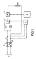
- Figure 1 depicts a degaussing circuit of a first embodiment of the invention.
- the display apparatus having the degaussing circuit of Figure 1 is connected to the mains via a plug P.
- the plug P is connected to the electrical circuitry of the display apparatus through a mains switch 1.
- the two electrical inputs E1, E2 outputs of the mains switch 1 thus carry an AC voltage of 110 V or 230 V.
- the first electrical input E1 is connected to a first pin of a first PTC resistor R1 and to a first pin of a second PTC resistor R2.
- the second pin of the first PTC resistor R1 and the second pin of the second PTC resistor R2 are respectively connected to a first input of a selector switch 6 and to a second input of this selector switch 6.
- the first PTC resistor R1 is suitable when the mains voltage (voltage between the electrical inputs E1, E2) is 110 V whereas the second PTC resistor R2 is suitable when the mains voltage is 230 V.
- An output of the selector switch 6 is connected to an input of a control switch 8.
- the output of the control switch 8 is connected to a first extremity of a degaussing coil DGC, which second extremity is connected to the second electrical input E2.
- the control switch 8 is controlled by a control circuit 4, for instance a micro-processor of the display apparatus.
- a voltage sensor circuit 2 is also connected to the electrical inputs E1 and E2 in order to measure the voltage difference between them (and thus the mains voltage supplying the apparatus) and to control the selector switch 6 depending on the measured voltage.
- R1 is a 5 ⁇ PTC resistor referenced BC96686 whereas R2 is a 26 ⁇ PTC resistor referenced BC96688 (for use with a degaussing coil DGC having a resistance of 25 ⁇ ).
- the mains switch 1 is closed by the user of the display apparatus at time to. At that time, a lot of transients may occur.
- the voltage sensor circuit 2 may not be able to operate correctly, on the one hand because it may not be correctly initialised yet and on the other hand because the voltage between the electrical inputs E1 and E2 may not be stabilised.
- the voltage sensor circuit 2 sends a control signal to the selector switch 6 depending on the voltage measured between electrical inputs E1 and E2. If the measured voltage is below 170 V, the voltage sensor circuit 2 controls the selector switch 6 so that it connects the first PTC resistor R1 to the control switch 8 (first input of the selector switch 6 selected). If the measured voltage is above 170 V, the voltage sensor circuit 2 controls the selector switch 6 so that it connects the second PTC resistor R2 to the control switch 8 (second input of the selector switch 6 selected).
- the control circuit 4 activates the degaussing operation by closing the control switch 8 as shown on Figure 2d.
- Time t 3 is later than time t 2 so that the correct PTC resistor (R1 or R2) is connected to the degaussing coil DGC from the beginning of the degaussing operation triggered by the control circuit 4 via the control switch 8.
- the degaussing operation lasts for a pre-determined period of time (t 4 - t 3 ) necessary for the decay of the degaussing current to take place thanks to the used PTC resistor (R1 or R2).
- a second embodiment of the invention is represented on Figure 3. Electrical inputs E1 and E2 are fed from the mains via a plug P and a mains switch 11. Two PTC resistors R are connected in parallel between electrical input E1 and a first pin of a control switch 18. In the described example, two identical PTC resistors R (Murata 9 ⁇ ) are used. Instead of 2 parallel PTC resistors, 2 PTC resistors connected in series or even a single PTC resistor could be used.
- the second pin of the control switch 18 is connected to a first input of a first path switch 17 through a first degaussing coil DGC1, to a second input of the first path switch 17 and to a first pin of a capacitor C.
- the first input of the first path switch 17 is also connected to a second input of a second path switch 15.
- the first input of the second path switch 15 is left unconnected.
- Electrical input E2 is connected to the output of the second path switch 15, to the output of the first path switch 17 through a second degaussing coil DGC2 and to the second pin of the capacitor C.
- Capacitor C (0.1 ⁇ F) is meant to reduce the impedance of the degaussing coils DGC1, DGC2 at the horizontal scanning frequency.
- the first degaussing coil DGC1 is a top degaussing coil whereas the second degaussing coil DGC2 is a bottom degaussing coil.
- DGC1 is the bottom degaussing coil and DGC2 the top degaussing coil.
- a voltage sensor 12 is connected to electrical inputs E1 and E2 in order to measure the voltage therebetween, determine the mains voltage and accordingly control the first and second path switches 15, 17 as further explained below.
- a controller 14 controls the control switch 18 to trigger the degaussing operation.
- the first and second path switches 15, 17 are controlled so that their second input contacts their output.
- the first degaussing coil DGC1 is then connected to electrical input E2 via the second path switch 15 and the second degaussing coil DGC2 is connected to the second pin of the control switch 18.
- the first and second degaussing coils DGC1, DGC2 are thus connected in parallel.
- the first and second path switches 15, 17 are controlled so that their first input contacts their output.
- the first and second degaussing coils DGC1, DGC2 are then connected in series between electrical input E2 and the second pin of the control switch 18.
- the impedance of the degaussing circuit is modified to best fit the mains voltage, i.e. to keep a slow decay time whatever the mains voltage.
- the degaussing operation is made by having the controller 14 close the control switch 18 for a predetermined period. This period can be determined as in the first embodiment so that the adapted connection is made between the degaussing coils DGC1, DGC2 (by use of the first and second path switches 15, 17) before the degaussing operation is triggered by the controller 14.
- the invention is of course not limited to the above embodiments. For instance, other values for the threshold voltage than 170 V or 180 V can be used.
Landscapes
- Engineering & Computer Science (AREA)
- Multimedia (AREA)
- Signal Processing (AREA)
- Video Image Reproduction Devices For Color Tv Systems (AREA)
Abstract
Description
- sensing said voltage ;
- selecting said impedance based on said voltage ;
- operating said degaussing circuit.
- the degaussing circuit has a voltage sensor circuit for measuring said voltage and at least one switch controlled by said voltage sensor circuit ;
- said switch selectively connects a first PTC resistor or a second PTC resistor in-circuit ;
- the degaussing circuit comprises a first degaussing coil and a second degaussing coil, and said first degaussing coil and said second degaussing coil are selectively connected in series or in parallel. Lastly, the invention proposes a process for degaussing a cathode ray tube with a degaussing circuit fed by a voltage, comprising the successive steps of :
- sensing said voltage ;
- selecting an impedance of said degaussing circuit based on said voltage ;
- supplying said voltage to said degaussing circuit.
- Figure 1 represents a degaussing circuit of a first embodiment of the invention ;
- Figures 2a to 2d are timing diagrams showing operation of various elements of the circuit of Figure 1 ;
- Figure 3 represents a degaussing circuit of a second embodiment of the invention.
Claims (10)
- Display apparatus with a cathode ray tube and a degaussing circuit fed by a voltage and comprising :characterized by means for selecting an impedance of the degaussing circuit based on said voltage.at least a PTC resistor (R1, R2 ; R) ;at least a degaussing coil (DGC ; DGC1, DGC2) ;
- Display apparatus according to claim 1, comprising a voltage sensor circuit (2 ; 12) for measuring said voltage and at least one switch (6 ; 15, 17) controlled by said voltage sensor circuit.
- Display apparatus according to claim 2, wherein said switch selectively connects a first PTC resistor (R1) or a second PTC resistor (R2) in the degaussing circuit.
- Display apparatus according to claim 2, wherein said degaussing circuit comprises a first degaussing coil (DGC1) and a second degaussing coil (DGC2) and wherein said first degaussing coil (DGC1) and said second degaussing coil (DGC2) are selectively connected in series or in parallel.
- Process for controlling a display apparatus according to claim 1, with the successive steps of :sensing said voltage (t1) ;selecting said impedance based on said voltage (t2) ;operating said degaussing circuit (t3).
- Degaussing circuit for a display apparatus with a cathode ray tube, the degaussing circuit being fed by a voltage and comprising :characterized by means for changing the impedance of the degaussing circuit based on said voltage.at least a PTC resistor (R1, R2 ; R) ;at least a degaussing coil (DGC ; DGC1, DGC2) ;
- Degaussing circuit according to claim 6, comprising a voltage sensor circuit (2 ; 12) for measuring said voltage and at least one switch (6 ; 15, 17) controlled by said voltage sensor circuit.
- Degaussing circuit according to claim 7, wherein said switch selectively connects a first PTC resistor (R1) or a second PTC resistor (R2) in-circuit.
- Degaussing circuit according to claim 7, comprising a first degaussing coil (DGC1) and a second degaussing coil (DGC2), wherein said first degaussing coil (DGC1) and said second degaussing coil (DGC2) are selectively connected in series or in parallel.
- Process for degaussing a cathode ray tube with a degaussing circuit fed by a voltage, comprising the successive steps of :sensing said voltage (t1) ;selecting an impedance of said degaussing circuit based on said voltage (t2) ;supplying said voltage to said degaussing circuit (t3).
Priority Applications (1)
| Application Number | Priority Date | Filing Date | Title |
|---|---|---|---|
| EP03300234A EP1441538A3 (en) | 2003-01-21 | 2003-11-28 | Display apparatus with a cathode ray tube, degaussing circuit for such a display apparatus and process for degaussing a cathode ray tube |
Applications Claiming Priority (3)
| Application Number | Priority Date | Filing Date | Title |
|---|---|---|---|
| EP03425022A EP1441539A1 (en) | 2003-01-21 | 2003-01-21 | Display apparatus with a cathode ray tube, degaussing circuit for such a display apparatus and processing for degaussing a cathode ray tube |
| EP03425022 | 2003-01-21 | ||
| EP03300234A EP1441538A3 (en) | 2003-01-21 | 2003-11-28 | Display apparatus with a cathode ray tube, degaussing circuit for such a display apparatus and process for degaussing a cathode ray tube |
Publications (2)
| Publication Number | Publication Date |
|---|---|
| EP1441538A2 true EP1441538A2 (en) | 2004-07-28 |
| EP1441538A3 EP1441538A3 (en) | 2006-06-14 |
Family
ID=32598819
Family Applications (1)
| Application Number | Title | Priority Date | Filing Date |
|---|---|---|---|
| EP03300234A Withdrawn EP1441538A3 (en) | 2003-01-21 | 2003-11-28 | Display apparatus with a cathode ray tube, degaussing circuit for such a display apparatus and process for degaussing a cathode ray tube |
Country Status (1)
| Country | Link |
|---|---|
| EP (1) | EP1441538A3 (en) |
Family Cites Families (2)
| Publication number | Priority date | Publication date | Assignee | Title |
|---|---|---|---|---|
| JPH0197091A (en) * | 1987-10-09 | 1989-04-14 | Mitsubishi Electric Corp | Automatic demagnetization circuit |
| JPH05153606A (en) * | 1991-11-27 | 1993-06-18 | Sony Corp | Degaussing circuit |
-
2003
- 2003-11-28 EP EP03300234A patent/EP1441538A3/en not_active Withdrawn
Also Published As
| Publication number | Publication date |
|---|---|
| EP1441538A3 (en) | 2006-06-14 |
Similar Documents
| Publication | Publication Date | Title |
|---|---|---|
| US8053933B2 (en) | Switching means for connecting a load to a power supply and its method of operation | |
| WO1996034510A2 (en) | Safety device for an electric heating appliance | |
| US4945210A (en) | Card controlled soldering iron temperature control device | |
| CA1239195A (en) | Start circuit for microwave oven | |
| KR101600124B1 (en) | Method and apparatus for detrrmination of electrical welding circuit variables | |
| RU2752849C2 (en) | Controlled release of the circuit breaker | |
| US4238711A (en) | Circuit for selective individual operation of multiple arc discharge lamps | |
| EP2028676A2 (en) | Automatically configuring vacuum contactor | |
| US9337616B2 (en) | Bias current control of laser diode instrument to reduce power consumption of the instrument | |
| GB2271894A (en) | Electric appliance | |
| US5812352A (en) | Circuit breaker tester | |
| CA2138905C (en) | Control for a toaster for varying the duration of the toasting cycle | |
| EP1441539A1 (en) | Display apparatus with a cathode ray tube, degaussing circuit for such a display apparatus and processing for degaussing a cathode ray tube | |
| US4990733A (en) | Microwave oven with improved microwave power control | |
| US4861967A (en) | Card controlled soldering iron temperature control device | |
| US5175413A (en) | Fail-safe relay drive system for cooking apparatus | |
| US4769556A (en) | Electronic clock timer for a kitchen range | |
| US5317115A (en) | Electronic control for a microwave oven | |
| TW201813230A (en) | Battery protection integrated circuit, protection circuit thereof and protection method | |
| WO2002052711A2 (en) | Improved method of controlling three phase motor starting sequence | |
| US4189665A (en) | Irradiation apparatus | |
| US6796297B2 (en) | Device for ignition of an internal combustion engine | |
| JPH08185931A (en) | Interface connection device and connection method thereof | |
| US4987556A (en) | Heating cooking appliance with relay testing | |
| GB2342723A (en) | Electrical appliance testing apparatus |
Legal Events
| Date | Code | Title | Description |
|---|---|---|---|
| PUAI | Public reference made under article 153(3) epc to a published international application that has entered the european phase |
Free format text: ORIGINAL CODE: 0009012 |
|
| AK | Designated contracting states |
Kind code of ref document: A2 Designated state(s): AT BE BG CH CY CZ DE DK EE ES FI FR GB GR HU IE IT LI LU MC NL PT RO SE SI SK TR |
|
| AX | Request for extension of the european patent |
Extension state: AL LT LV MK |
|
| RAP1 | Party data changed (applicant data changed or rights of an application transferred) |
Owner name: THOMSON LICENSING |
|
| PUAL | Search report despatched |
Free format text: ORIGINAL CODE: 0009013 |
|
| AK | Designated contracting states |
Kind code of ref document: A3 Designated state(s): AT BE BG CH CY CZ DE DK EE ES FI FR GB GR HU IE IT LI LU MC NL PT RO SE SI SK TR |
|
| AX | Request for extension of the european patent |
Extension state: AL LT LV MK |
|
| 17P | Request for examination filed |
Effective date: 20061207 |
|
| AKX | Designation fees paid |
Designated state(s): DE FR GB |
|
| 17Q | First examination report despatched |
Effective date: 20070413 |
|
| STAA | Information on the status of an ep patent application or granted ep patent |
Free format text: STATUS: THE APPLICATION IS DEEMED TO BE WITHDRAWN |
|
| 18D | Application deemed to be withdrawn |
Effective date: 20071027 |