EP1441444A1 - Method of correction of the error introduced by a multibit DAC incorporated in aN ADC - Google Patents
Method of correction of the error introduced by a multibit DAC incorporated in aN ADC Download PDFInfo
- Publication number
- EP1441444A1 EP1441444A1 EP03425032A EP03425032A EP1441444A1 EP 1441444 A1 EP1441444 A1 EP 1441444A1 EP 03425032 A EP03425032 A EP 03425032A EP 03425032 A EP03425032 A EP 03425032A EP 1441444 A1 EP1441444 A1 EP 1441444A1
- Authority
- EP
- European Patent Office
- Prior art keywords
- dac
- error
- scrambling
- adc
- calculating
- Prior art date
- Legal status (The legal status is an assumption and is not a legal conclusion. Google has not performed a legal analysis and makes no representation as to the accuracy of the status listed.)
- Granted
Links
Images





Classifications
-
- H—ELECTRICITY
- H03—ELECTRONIC CIRCUITRY
- H03M—CODING; DECODING; CODE CONVERSION IN GENERAL
- H03M1/00—Analogue/digital conversion; Digital/analogue conversion
- H03M1/06—Continuously compensating for, or preventing, undesired influence of physical parameters
- H03M1/0617—Continuously compensating for, or preventing, undesired influence of physical parameters characterised by the use of methods or means not specific to a particular type of detrimental influence
- H03M1/0634—Continuously compensating for, or preventing, undesired influence of physical parameters characterised by the use of methods or means not specific to a particular type of detrimental influence by averaging out the errors, e.g. using sliding scale
- H03M1/0656—Continuously compensating for, or preventing, undesired influence of physical parameters characterised by the use of methods or means not specific to a particular type of detrimental influence by averaging out the errors, e.g. using sliding scale in the time domain, e.g. using intended jitter as a dither signal
- H03M1/066—Continuously compensating for, or preventing, undesired influence of physical parameters characterised by the use of methods or means not specific to a particular type of detrimental influence by averaging out the errors, e.g. using sliding scale in the time domain, e.g. using intended jitter as a dither signal by continuously permuting the elements used, i.e. dynamic element matching
- H03M1/0673—Continuously compensating for, or preventing, undesired influence of physical parameters characterised by the use of methods or means not specific to a particular type of detrimental influence by averaging out the errors, e.g. using sliding scale in the time domain, e.g. using intended jitter as a dither signal by continuously permuting the elements used, i.e. dynamic element matching using random selection of the elements
-
- H—ELECTRICITY
- H03—ELECTRONIC CIRCUITRY
- H03M—CODING; DECODING; CODE CONVERSION IN GENERAL
- H03M1/00—Analogue/digital conversion; Digital/analogue conversion
- H03M1/12—Analogue/digital converters
- H03M1/14—Conversion in steps with each step involving the same or a different conversion means and delivering more than one bit
- H03M1/16—Conversion in steps with each step involving the same or a different conversion means and delivering more than one bit with scale factor modification, i.e. by changing the amplification between the steps
- H03M1/164—Conversion in steps with each step involving the same or a different conversion means and delivering more than one bit with scale factor modification, i.e. by changing the amplification between the steps the steps being performed sequentially in series-connected stages
- H03M1/167—Conversion in steps with each step involving the same or a different conversion means and delivering more than one bit with scale factor modification, i.e. by changing the amplification between the steps the steps being performed sequentially in series-connected stages all stages comprising simultaneous converters
- H03M1/168—Conversion in steps with each step involving the same or a different conversion means and delivering more than one bit with scale factor modification, i.e. by changing the amplification between the steps the steps being performed sequentially in series-connected stages all stages comprising simultaneous converters and delivering the same number of bits
-
- H—ELECTRICITY
- H03—ELECTRONIC CIRCUITRY
- H03M—CODING; DECODING; CODE CONVERSION IN GENERAL
- H03M1/00—Analogue/digital conversion; Digital/analogue conversion
- H03M1/66—Digital/analogue converters
- H03M1/74—Simultaneous conversion
-
- H—ELECTRICITY
- H03—ELECTRONIC CIRCUITRY
- H03M—CODING; DECODING; CODE CONVERSION IN GENERAL
- H03M3/00—Conversion of analogue values to or from differential modulation
- H03M3/30—Delta-sigma modulation
- H03M3/458—Analogue/digital converters using delta-sigma modulation as an intermediate step
- H03M3/464—Details of the digital/analogue conversion in the feedback path
Definitions
- the present invention relates in general to the field of analog/digital conversion circuits or converters (ADCs), particularly to ADCs featuring high resolution and wide band.
- ADCs analog/digital conversion circuits or converters
- DACs digital/analog converters
- pipelined architecture the ADCs with sigma-delta architecture with multibit quantizers
- MASH architecture the ADCs with MASH architecture.
- a disadvantage in the implementation of these ADC structures is the error introduced in the converted signal by the multibit DACs.
- error derives from the inevitable mutual differences between the one-bit conversion elements composing the multibit DAC, and translates in a non-linearity of the ADC.
- the linearity requirements for the multibit DAC located downstream the flash ADC in the first ADC stage coincide with those for the whole converter, since the linearity error introduced by the DAC acts in the same position as the signal to be converted.
- Mutual differences between the one-bit conversione elements of the multibit DAC for instance formed by switched-capacitor circuits, cause the lowering of the signal/noise and distorsion ratio (SNDR) and the reduction of the spurious-free dynamic range (SFDR) of the ADC, because of the appearance of a harmonic distorsion.
- US 2002/0041248 A1 describes a method of cancellation of the error introduced by the DAC of the first stage of a pipelined ADC.
- the DAC includes a digital encoder that randomly permutes the connections between the outputs of the flash ADC and the one-bit conversion elements of the DAC.
- a digital noise cancellation logic circuit for the cancellation of the noise the introduced by the DAC is provided; such circuit receives the random bits controlling the encoder, parity bits and the digital residue sum of the digital outputs of the stages downstream, and produces an estimation of the error introduced by the first stage.
- Such an estimation, subtracted from the digital signal produced by the stages downstream, is calculated by performing an average over a number of samples equal to at least 2 25 .
- the noise estimation is made possible thanks to the adoption of a well precise and rigid permutation law of the connections between the outputs of the flash ADC and the one-bit conversion elements of the DAC.
- the Applicant has also observed that the method of error estimation described in such a document, requiring an average over a very large number of samples, is rather slow.
- the time required by ADC output to converge to the corrected value is therefore rather long. For instance, if the ADC operates at a frequency of 80 MHz, the convergence time could be of the order of 1 second.
- FIG. 1 a functional block diagram of a multistage pipelined ADC according to an embodiment of the present invention is shown in FIG. 1.
- the pipelined ADC globally identified by 100, receives in input an analog signal In, for instance an electric voltage, and provides at the output thereof a corresponding digital signal Out, constituted by a prescribed number of bits, representing the binary-coded value of the input signal In.
- the pipelined ADC includes a plurality of cascaded analog/digital conversion stages, each stage having a respective conversion resolution.
- the pipelined ADC includes four stages 105-1, 105-2, 105-3 and 105-4, each having a conversion resolution equal to three bits, so that the ADC 100 has a relatively low overall resolution of nine bits; it is however noted that the beneficial effects of the error estimation and correction method are appreciated the better the higher the resolution of the ADC; in particular, such beneficial effects can be clearly appreciated in ADCs with resolution equal to or higher than thirteen bits.
- the first stage 105-1 receives the analog input signal In, performs an analog/digital conversion thereof with resolution of three bits, producing a digital signal Out1 of three bits, and feeds the second stage 105-2 with a first residual analog signal Res1, equal to the difference between the analog input signal In and an analog signal corresponding to the digital signal Out1.
- the second stage 105-2 performs on the residual analog signal Res1 the same operations that the first stage 105-1 performs on the analog input signal In, producing a digital signal Out2 of three bits and a second residual analog signal Res2.
- the third stage 105-3 receives the second residual analog signal Res2, performs an analog/digital conversion thereof with resolution of three bits producing a digital signal Out3 of three bits, and feeds the fourth stage 105-4 with a third residual analog signal Res3, equal to the difference between the second residual analog signal Res2 and an analog signal corresponding to the digital signal Out3.
- the fourth and last stage 105-4 receives the third residual analog signal Res3 and performs an analog/digital conversion thereof with resolution of three bits, producing a digital signal Out4 of three bits.
- the first stage 105-1 includes a sample-and-hold circuit 110, periodically sampling the analog input signal In.
- An output Ins of the sample-and-hold circuit 110, or sampled analog signal, representing the value of the analog input signal In at a given sampling instant, is fed to a nine-levels flash ADC 115; conventionally, the flash ADC 115 includes eight comparator circuits, for instance voltage comparators, that compare the sampled analog signal Ins to a set of eight voltage references.
- the output Th-Out1 of the flash ADC 115 comprising eight digital signals, is made up of the output of the eight comparator circuits of the ADC 115, and provides what in jargon is called a thermometric representation or coding of the converted sampled analog signal.
- thermometric coded output Th-Out1 of the ADC 115 is fed to a thermometric-binary converter 120, that converts the thermometric representation of the converted analog signal into a binary representation, for instance in two's complement, producing the digital signal Out1.
- the thermometric coded output Th-Out1 of the ADC 115 is also fed to a nine-levels multibit DAC 125, comprising eight single-bit DACs, for instance of the switched-capacitor type.
- the output ODAC of the DAC 125 is an analog signal derived from the digital/analog conversion of the thermometric coded output Th-Out1 of the ADC 115; the output ODAC of the DAC 125 is subtracted from the sampled analog signal Ins in a subtractor circuit 130; the difference analog signal thus obtained is fed to an interstage amplifier 135, that outputs the residual analog signal Res1 fed to the second stage 105-2.
- the stages 105-2 and 105-3 have a structure similar to that of the first stage 105-1: the respective digital signals Out2 and Out3 and the respective residual analog signals Res2 and Res3 are produced in way similar to the digital signal Out1 and the residual analog signal Res1.
- the fourth and last stage 105-4 of the ADC 1 differs from the stages upstream in that it only comprises the sample-and-hold circuit 110, the ADC 115 and the thermometric-binary converter 120, that converts the thermometric coded output Th-Out4 of the respective ADC 115 into the digital signal Out4, without including the elements for the generation of the residual analog signal.
- the digital signals Out2, Out3 and Out4 are added in an adder 140, that provides a sum digital signal Res1d, constituting a digital representation of the residual analog signal Res1 of the first stage 105-1.
- the one-bit conversion elements of the DAC 125 should ideally be identical to each other. Nevertheless, in the practice such one-bit conversion elements of the multibit DAC 125 inevitably show mutual differences, that make them more or less different from one another; for instance, in an implementation of the DAC 125 by means of switched-capacitor circuits, it is not possible to have condensers with identical capacitance values. Such mutual differences between the one-bit elements of the DAC 125 introduce an error, referred to as linearity error or distortion, in the digital/analog conversion of the thermometric coded digital signal Th-Out1.
- the linearity error introduced by the DAC 125 affects the residual analog signal Res1, and therefore the digital signal Resd1, constituting the digital conversion thereof.
- the digital signal Res1d is fed to a block 145 of estimation and correction of the linearity error introduced by the DAC 125 of the first stage 105-1.
- the error estimation and correction block 145 provides a digital signal Res1dc, constituting a digital representation of the residual analog signal Res1 substantially freed of the linearity error introduced by the DAC 125.
- the digital signal Out1 provided by the first stage 105-1 and the digital signal Res1dc provided by the block 145 are added to each other in an adder 150, to generate the output digital signal Out of the ADC 100.
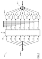
- FIG. 2 is a more detailed view of the DAC 125.
- the eight signals th1 - th8 constituting the thermometric coded digital signal Th-Out1 produced by the ADC 115 are fed to a permutation or scrambling block 200.
- the scrambling block 200 performs a scrambling of the eight signals th1 - th8, according to a given law and depending on the values of a group R of variables, generated for instance by the estimation and correction block 145. Particularly, the values assigned to the variable of the group R are substantially random or pseudorandom, so that the scrambling of the signals performed by the scrambling block 200 is substantially random.
- the scrambling block 200 outputs eight signals t1 - t8, constituting a scrambled representation of the original eight signals th1 - th8; each of the eight signals t1 - t8 is fed to a respective single-bit DAC, or one-bit conversion element of the multibit DAC 125, 205-1 - 205-8.
- the scrambling block 200 performing a scrambling of the signals th1 - th8 in dependence of the pseudorandom values of the variables of the group R, avoids that a rigid association exists between any given combination of "1"s and "0"s in the digital signal Th-Out1 and the one-bit DACs 205-1-205-8.
- the scrambling block 200 substantially makes the association of a given DAC 205-1 - 205-8 with a given signal th1 - th8 random. Thanks to the presence of the scrambling block 200, the harmonic distortion effect induced by the mutual differences between the one-bit conversion elements 205-1 - 205-8 of the DAC 125 is reduced.
- the error estimation and correction block 145 is able to estimate and correct the linearity error introduced by the DAC 125.
- the following theoretical discussion will enable to understand the error estimation and correction method according to the present invention.
- the value e i defines therefore the error committed by the i th one-bit conversion element u i of the multibit DAC.
- the so-called gain error of the multibit DAC due to the fact that the average of the values of the one-bit conversion elements is not equal to 1 but to a different value u v , is not taken in consideration. However, such a gain error does not contribute to the linearity error E DAC .
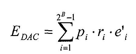
- the generic linearity error E DAC can be represented by a linear combination of the single errors e i : where the coefficients t i of the linear combination have values equal to 0 or +1 depending on whether the i th one-bit conversion element of the DAC has to convert a logic "0" or a logic "1".
- the group of coefficients t i constitutes therefore the thermometric coded digital signal Th-Out1 produced by the ADC 115 and scrambled by the scrambling block 200, i.e. the digital signals t1 - t8.
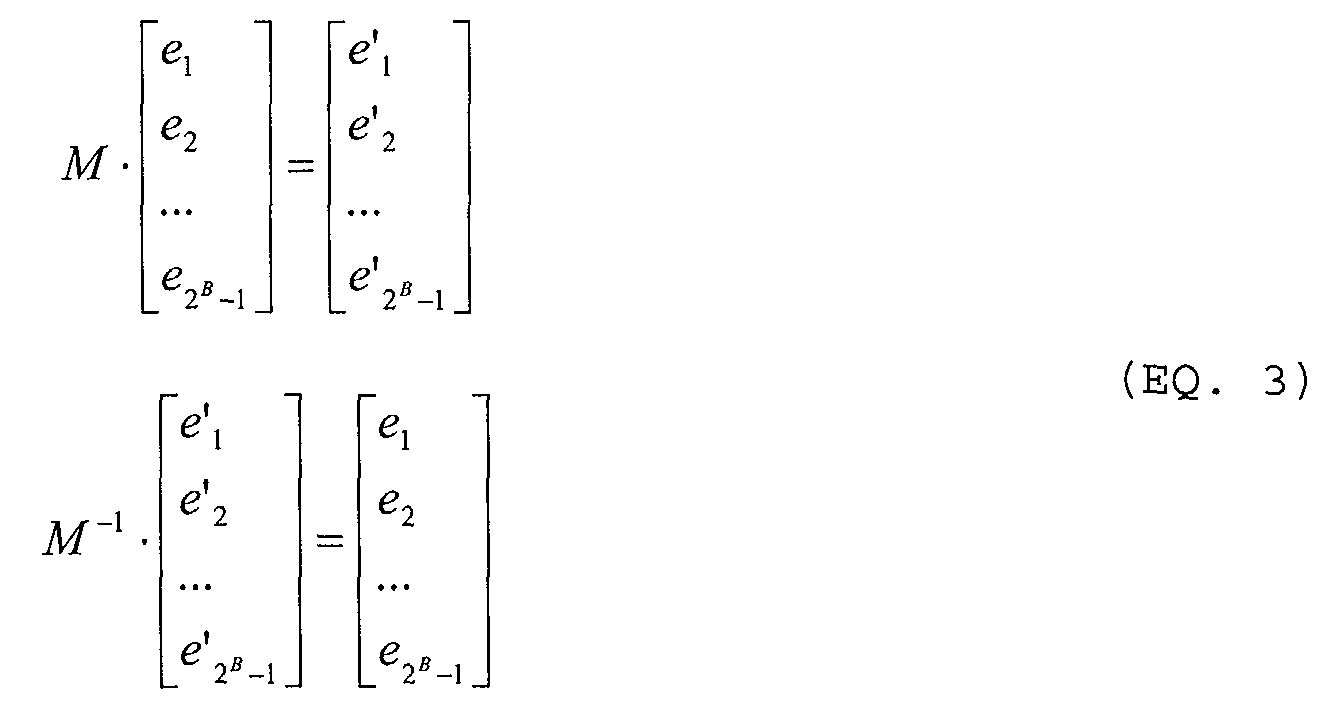
- the random or substantially random scrambling performed by the scrambling block 200 is therefore assimilated to a bilinear transformation, represented by an invertible matrix M ; known the matrix M and known the pseudorandom variables, it is possible to represent the linearity error E DAC committed by the multibit DAC 125 in a new base of vectors ⁇ ' in which each coefficient ⁇ ' i of the linear combination contains, in addition to the information on the analog-converted digital signal converted from the DAC 125, the information on the random or substantially random values of the variables R; operating such transformation, and calculating the coefficients of the linear combination, the estimation and correction block 145 will be able to extract the estimation of each vector e' i of the new base, and therefore to estimate the linearity error E DAC.
- a bilinear transformation represented by an invertible matrix M ; known the matrix M and known the pseudorandom variables
- any matrix M can be used, but not all the matrixes can be practically implemented in simple and fast way; on the other hand, the scrambling performed by the scrambling block 200 has to be relatively fast.
- the linearity error E DAC can be expressed as: so that the residual analog signal Res1 can be expressed as:
- thermometric coded digital signal produced by the ADC 115 A method according to the present invention will now be described for the generation and implementation of scrambling blocks of the thermometric coded digital signal produced by the ADC 115, adapted to allow the estimation and the correction of the linearity error.
- the scrambling block 200 is in general composed by a number of scrambling stages equal to the number of digital signals constituting the thermometric coded digital signal Th-Out1 provided by the ADC 115, minus one; such scrambling stages are connected in cascade in a tree configuration.
- the first scrambling stage receives the thermometric code outputted by the ADC 115, i.e. the signals making up the signal Th-Out1.
- a grouping criterion is then identified for grouping the bits outputted by the first scrambling stage. Also such criterion can be whatsover, but it has however to allow grouping the bits at the output of the first scrambling stage in two separated subsets, independently from the value taken by the variable r 1 , i.e. independently from the type of solution of the aforesaid scrambling law.
- the two separated subsets of bits are each fed to a respective scrambling stage downstream, that performs the same function of the first stage on the basis of the value of a respective variable of the group R, but on half the number of bits.
- the number of necessary scrambling stages and the number of variables of the group R are both equal to 2 B -1, where B is the number of bits resolved by the DAC 125, i.e. the number signals constituting the thermometric code outputted by the ADC 115.
- a graph identifying the interconnections of the various scrambling stages of the block 200 is built; such a graph describes the path that the first bit (th1 in the example of FIG. 2) of the thermometric code Th-Out1 inputted to the scrambling block 200 has to follow for reaching a prescribed position in the output code (t1 - t8) from the scrambling block 200; the nodes of the graphs represent the scrambling stages of the scrambling block 200.
- a matrix is built (matrix of incidence of the graph), of dimension 2 B -1 X 2 B -1, that corresponds to the above described inverse matrix M - 1 .
- the i th row of the matrix thus built describes the path that the first bit th1 in the thermometric code Th-Out1 inputted to the scrambling block 200 has to follow for reaching the i th position in the output code.
- a value equal to 1 or -1 is placed, according to the value that the variable r j , associated with j th scrambling stage passed through, has to take for obtaining the desired path; on all the other matrix columns, corresponding to the nodes of the graph that are not passed through, a value equal to 0 is placed.
- the matrix thus built will be used by the estimation block 145 to estimate and correct the linearity error, as will be described in greater detail later on.
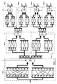
- the scrambling block 200 includes seven scrambling stages 300-1 - 300-7, each one controlled by the value of a respective variable r 1 - r 7 of the group R.
- the scrambling law used in the various scrambling stages is the following:
- the grouping criterion of the bits outputted by each scrambling stage calls for dividing the bits in two equal parts without modifying the order thereof.
- the interconnections graph obtainable from the scrambling block of FIG. 3 is shown in FIG. 4. On the basis of such interconnections graph, the following matrix of incidence is obtained, in the way described in the foregoing:
- a second exemplary practical embodiment of scrambling block 200 is shown in FIG. 5.
- the scrambling block 200 includes again seven scrambling stages 500-1 - 500-7, each one controlled by the value of a respective variable r 1 - r 7 of the group R.
- the scrambling law in the various scrambling stages is the same one used in the scrambling block of FIG. 3. Nevertheless, the grouping criterion of the bits outputted by each scrambling stage is a different one, in this case calling for the separation of the bits in even positions from those in odd positions.
- the scrambling block 200 again includes seven scrambling stages 700-1 - 700-7, each one controlled by the value of a respective pseudorandom variable r 1 - r 7 of the group R.
- the scrambling law used in the different scrambling stages is:
- the grouping criterion of the bits outputted from each scrambling stage calls for dividing the bits in two equal parts without modifying the order thereof.
- the error estimation block 145 After having built the matrix of incidence M - 1 , extrapolating it from the scrambling block 200 in the way previously described, such matrix (i.e. , the parameters that compose it) is stored in the error estimation block 145.
- the error estimation block 145 also receives from the DAC 125 the signals t 1 , t 2 ,..., t 8 outputted by the scrambling block 200.
- FIG. 9 shows, in terms of functional blocks, the error estimation block 145, in an embodiment of the present invention.
- a pseudorandom bit generator block 900 produces random or substantially random values to be assigned to the seven variables r 1 , r 2 ,..., r 7 , that are fed to the DAC 125 to drive the stages of the scrambling block 200; the block 900 is for instance implemented by means of a pseudorandom number generator (also known as linear feedback shift register). It is observed that, in general terms, the requirements on the values of the variables r 1 , r 2 ,..., r 7 are that they are uncorrelated to each other and to the input signal In to the ADC.
- the same variables r 1 , r 2 ,..., r 7 are also fed to an arithmetic calculation block 905, that additionally receives the eight signals t 1 , t 2 ,..., t 8 outputted by the scrambling block 200.
- the arithmetic calculation block 905 additionally calculates the matrix R - 1 ( i.e. , the inverse matrix of the diagonal matrix R containing the values of the pseudorandom variables r 1 , r 2 ,..., r 7 ), and, performing a matrix product, it determines the values p 1 , p 2 ,..., p 7 , containing the information on the analog signal converted by the flash ADC 115.
- the arithmetic calculation block 905 has to perform matrix calculations
- the calculations that the block 905 has to perform may reduce to simple products and additions or subtractions.
- choosing as possible values for the pseudorandom variables the values +1 and -1, the calculations that the block 905 has to perform may reduce to straight additions or subtractions; the block 905 can therefore be implemented by means of a suitable arrangement of adders, and the structure thereof is determined once that the matrix of incidence associated with the scrambling block 200 has been derived.
- Each of the values p 1 , p 2 ,..., p 7 thus calculated is fed, together with the associated variable r 1 , r 2 ,..., r 7 and the signal Res1dc, outputted by the block 145, to a respective correlation block 910-1, 910-2,..., 910-7.
- the respective value p i , the respective pseudorandom variable r i and the signal Resldc are multiplied in a multiplier 915 and the resulting product p i r i Res1dc is fed to a block 920 adapted to perform a weighted average of the product p i r i Res1dc over a prescribed number of sampling periods of the input signal In to the ADC 100 (therefore, on a prescribed number of samples of the input signal), for instance equal to 1024.
- the operations performed by the multiplier 915 and the block 920 correspond to an operation of correlation between the value p i , the pseudorandom variable r i and the signal Res1dc; the block 920 extracts therefore from the signal Res1dc an estimation ⁇ e'i> of the generic vector component e ' i of the error E DAC .
- the output of the block 920 provides an approximate estimation ⁇ e' i > of the component vector e ' i of the error E DAC ⁇
- a weight factor ⁇ is applied to the approximate estimation ⁇ e' i >, and the weighted approximate estimation ⁇ e' i > thus obtained is added, in an accumulator or integrator 930, to the weighted approximate estimations calculated in previous sampling periods.
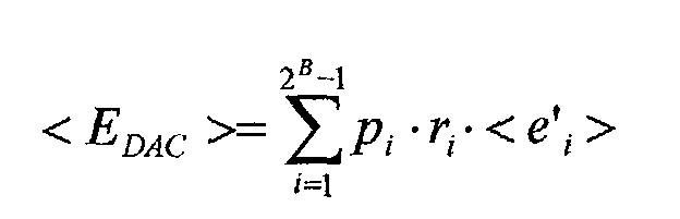
- an accumulated estimation ⁇ e' icum > of the vector e' i is therefore made available, and such accumulated estimation is fed, together with the respective value p i and the respective pseudorandom variable r i , to a multiplier 935 that therefore provides an estimation p i r i ⁇ e' icum > of the i th component of the linear combination corresponding to the estimation ⁇ E DAC > of the linearity error:
- each correlation block 910-1,..., 910-8, through a correlation process provides an estimation of a respective component of the linearity error E DAC ⁇
- the value of the signal Res1dc coincides with that of the signal Res1d, because the estimated value ⁇ e' i > for the generic error e ' i is zero.
- the signal Res1dc i.e. the signal Res1d corrected
- the signal Res1dc is fed back to the correlation blocks, so that the estimation is performed iteratively, producing more and more precise estimations of the respective component of the linearity error, converging toward a steady-state estimation that substantially coincides with the actual component of the error.
- the estimated value ⁇ e' icum > tends to the real value of the error e ' i .
- an approximate estimation of the error is already available, that allows to operate a correction of the signal Resld.
- it is possible to track relatively fast variations of the error E DAC for instance due to thermal drifts of the components of the DAC 125.
- FIG. 10 shows a functional block diagram of the block 920 of FIG. 9, in an embodiment of the present invention.
- it is a first-order filter, conceptually similar to a sinc filter, comprising an accumulator 1000 in which the values of the product p 1 r 1 Res1dc are accumulated.
- the output of the accumulator 1000 is fed to a down-sampler block 1005, operating on the basis of a frequency equal to the sampling frequency of the input signal divided by a prescribed factor n , for example equal to 1024.
- n for example equal to 1024.
- the value of the accumulator 1000 at the generic sampling period k is then subtracted from the value of the accumulator at the sampling period k+n.
- the average is not performed dividing the value provided by the block 1010 by the number n of sampling periods: the value provided by the block 1010 is instead normalized dividing it, in the block 1015, by the integral, calculated on the n sampling periods, of the square modulus of the value p i ; in this way, the convergence of the estimation of the errors takes place with one time constant only, adjustable through the weight factor ⁇ .
- the weight factor ⁇ can be chosen to have a value equal to a power of two, in the range 2 -8 to 2 -14 ; the specific value of the weight factor ⁇ can be chosen by the designer on the basis of the ADC ( e.g. , on the resolution thereof).
- the described error correction method has the advantage of not being limited to a fixed, rigid scrambling scheme of the thermometric coded signals outputted by the flash ADC 115. Any scrambling scheme can in principle be adopted.
- Another advantage resides in the fact that the estimation of the error is performed iteratively, producing more and more precise estimations of the error, averaging over a relatively small number of sampling periods. This allows a relatively fast convergence of the ADC output signal toward the value purged by the error of the DAC, and also allows following dynamic variations of the DAC error. Simulations conducted by the Applicant have shown that, at a sampling frequency of 80 MHz, the time necessary for the convergence is lower than 50 ms.
- a non negligible aspect is that the above advantages, as well other advantages, are achieved with a relatively small circuit complexity.
- the present invention can also find application in other types of ADC, for instance in sigma-delta or MASH architectures.
- the signal containing the error introduced by the multibit DAC, to be used for the estimation of the error can be the output signal of the converter; in the case of a multistage MASH converter, having a first stage constituted by a multibit sigma-delta converter, the signal containing the error introduced by the multibit DAC, to be used for the estimation, can be the output signal of the first stage of the converter, i.e. the output signal of the sigma-delta converter.
- any digital signal produced by the ADC and that contains such error can be used for the estimation of the error introduced by a multibit DAC incorporated in an ADC.
Landscapes
- Engineering & Computer Science (AREA)
- Theoretical Computer Science (AREA)
- Analogue/Digital Conversion (AREA)
Abstract
Description






Claims (7)
- A method of correction of the error in an output digital signal (Out) of an analog/digital converter (ADC) (100), in which said error is introduced by a multibit digital/analog converter (DAC) (125) incorporated in the ADC, comprising:providing a scrambling scheme (200) of input signals (th1-th8) to the DAC, said scrambling scheme defining a scrambling of the input signals as a function of values of a group (R) of variables (r1-r7), to produce scrambled input signals (t1-t8);extrapolating from the scrambling scheme parameters (M - 1 ) defining a transformation operated by the scrambling scheme on the input signals to obtain the scrambled input signals;assigning to said variables values substantially uncorrelated to each other;on the basis of said parameters, of said substantially uncorrelated values and of said scrambled signals, calculating (905) coefficients (pi, piri) of a linear combination of vectors of a vector space, said linear combination of vectors corresponding to a vector of the vector space representative of the error introduced by the multibit DAC;calculating (910-1,..., 910-7) the correlation of a signal (Res1d) containing the error introduced by the multibit DAC with each coefficient of the linear combination of vectors, to extract an estimation (<e'icum>) of each of said vectors;on the basis of said coefficients and of said estimations of the vectors, calculating a linear combination (piri<e'icum>) representative of the estimation of the error introduced by the multibit DAC; andusing said estimation of the error introduced by the multibit DAC to correct the output signal of the ADC.
- The method according to claim 1, in which said calculating the correlation includes:iterating the actions a) and b).a) calculating approximate estimations (<e' i>) of each vector by calculating said correlation on a prescribed number of sampling periods,b) correcting the signal containing the error through said approximate estimations, and
- Method according to claim 2, in which said calculating approximate estimations includes, for each vector, calculating averages, on said prescribed number of sampling periods, of products (PiriRes1dc) of said coefficients by the signal containing the error.
- Method according to claim 3, in which said calculating averages includes:accumulating in an accumulator (1000) said products;obtaining (1005) from said accumulator pairs of values accumulated at a distance of said prescribed number of sampling periods;obtaining (1010) a difference value of each pair of values; anddividing the difference value for an accumulated value of the respective coefficient.
- Method according to claim 4, in which said calculating approximate estimations includes applying to each average on the prescribed number of sampling periods a pre-determined weight factor (µ), to get a weighted average (µ<e' i >), and accumulating the weighted averages in an accumulator (930).
- Method according to claim 1, in which said providing the scrambling scheme includes:a) providing a permutation law of the input signals to the DAC, in which said law has a first type of permutation and a second type of permutation mutually alternative, the first type of permutation being triggered by a first value assigned to a respective first variable (r1), and the second type of permutation being triggered by a second value assigned to the respective first variable;b) grouping the permuted signals in two separated sets of signals;c) permuting the signals of each set on the basis of said law, depending on values assigned to respective second (r2) and third (r3) variable;d) repeating the actions b) and c), permuting the signals on the basis of said law, each time as a function of values assigned to further variables, until said two separated sets contains only one signal each.
- Device of correction of the error in an output digital signal (Out) of an analog/digital converter (ADC) (100), in which said error is introduced by a multibit digital/analog converter (DAC) (125) incorporated in the ADC, comprising:scrambling means (200) to produce, starting from input signals (th1-th8) to the multibit DAC, scrambled input signals (t1-t8) as a function of values assigned to a group (R) of variable (r1-r7), said scrambling means having associated therewith parameters (M-1 ) defining a transformation operated by the scrambling means;means (900) for assigning to said variables substantially uncorrelated values;calculation means (905) for calculating, on the basis of said parameters, of said substantially uncorrelated values and of said scrambled signals, coefficients (p i ) of a linear combination of vectors of a vector space, said linear combination of vectors corresponding to a vector of the vector space representative of the error introduced by the DAC;correlation means (910-1,...,910-7) for calculating the correlation of a signal (Res1d) containing the error introduced by the multibit DAC with each coefficient of the linear combination of vectors, to extract estimations of each of said vectors,means (935,940) for calculating a linear combination representative of the estimation of the error introduced by the multibit DAC and to correct the ADC output signal on the basis of said estimation of the error.
Priority Applications (3)
| Application Number | Priority Date | Filing Date | Title |
|---|---|---|---|
| DE60312808T DE60312808D1 (en) | 2003-01-24 | 2003-01-24 | Method for correcting the error caused by a multi-bit DA converter in an AD converter |
| EP03425032A EP1441444B1 (en) | 2003-01-24 | 2003-01-24 | Method of correction of the error introduced by a multibit DAC incorporated in aN ADC |
| US10/764,128 US6867718B2 (en) | 2003-01-24 | 2004-01-23 | Method of correction of the error introduced by a multibit DAC incorporated in an ADC |
Applications Claiming Priority (1)
| Application Number | Priority Date | Filing Date | Title |
|---|---|---|---|
| EP03425032A EP1441444B1 (en) | 2003-01-24 | 2003-01-24 | Method of correction of the error introduced by a multibit DAC incorporated in aN ADC |
Publications (2)
| Publication Number | Publication Date |
|---|---|
| EP1441444A1 true EP1441444A1 (en) | 2004-07-28 |
| EP1441444B1 EP1441444B1 (en) | 2007-03-28 |
Family
ID=32524305
Family Applications (1)
| Application Number | Title | Priority Date | Filing Date |
|---|---|---|---|
| EP03425032A Expired - Lifetime EP1441444B1 (en) | 2003-01-24 | 2003-01-24 | Method of correction of the error introduced by a multibit DAC incorporated in aN ADC |
Country Status (3)
| Country | Link |
|---|---|
| US (1) | US6867718B2 (en) |
| EP (1) | EP1441444B1 (en) |
| DE (1) | DE60312808D1 (en) |
Cited By (1)
| Publication number | Priority date | Publication date | Assignee | Title |
|---|---|---|---|---|
| CN108900195A (en) * | 2018-07-03 | 2018-11-27 | 清华大学深圳研究生院 | Oversampling analog-to-digital converter and its feedback digital analog converter dynamic error calibration method |
Families Citing this family (10)
| Publication number | Priority date | Publication date | Assignee | Title |
|---|---|---|---|---|
| DE60307226D1 (en) * | 2003-02-18 | 2006-09-14 | St Microelectronics Srl | Analog-to-digital converter with correction of shift errors |
| US6937176B2 (en) * | 2003-09-30 | 2005-08-30 | Koninklijke Philips Electronics, N.V. | Ultrasonic signal acquisition in the digital beamformer |
| US7586429B1 (en) * | 2006-05-09 | 2009-09-08 | Marvell International Ltd. | Scrambling system for high resolution ditigal-to-analog converter |
| US8385498B2 (en) * | 2006-05-31 | 2013-02-26 | Kenet, Inc. | Boosted charge transfer circuit |
| WO2008088877A2 (en) * | 2007-01-19 | 2008-07-24 | Kenet, Inc. | Charge-domain pipelined analog-to-digital converter |
| EP2106586B1 (en) * | 2007-01-23 | 2014-11-12 | Kenet, Inc. | Analog error correction for a pipelined charge-domain a/d converter |
| RU2352060C1 (en) * | 2007-05-29 | 2009-04-10 | Ставропольский военный институт связи ракетных войск | Method and device of correction of analog-digital transformation errors |
| US8279955B1 (en) | 2008-01-15 | 2012-10-02 | Marvell International Ltd. | Systems and methods for calibrating digital baseband DC offset in an OFDM receiver |
| US8791844B2 (en) * | 2011-06-09 | 2014-07-29 | Microchip Technology Incorporated | Modified dynamic element matching for reduced latency in a pipeline analog to digital converter |
| US8497789B2 (en) * | 2011-06-10 | 2013-07-30 | Microchip Technology Incorporated | Modified dynamic element matching for reduced latency in a pipeline analog to digital converter |
Citations (1)
| Publication number | Priority date | Publication date | Assignee | Title |
|---|---|---|---|---|
| US20020041248A1 (en) * | 2000-02-22 | 2002-04-11 | Ian Galton | Digital cancellation of D/A converter noise in pipelined A/D converters |
Family Cites Families (1)
| Publication number | Priority date | Publication date | Assignee | Title |
|---|---|---|---|---|
| US6049298A (en) * | 1996-12-23 | 2000-04-11 | National Instruments Corp. | System and method for generating a linearity error correction device for an analog to digital converter |
-
2003
- 2003-01-24 EP EP03425032A patent/EP1441444B1/en not_active Expired - Lifetime
- 2003-01-24 DE DE60312808T patent/DE60312808D1/en not_active Expired - Lifetime
-
2004
- 2004-01-23 US US10/764,128 patent/US6867718B2/en not_active Expired - Lifetime
Patent Citations (1)
| Publication number | Priority date | Publication date | Assignee | Title |
|---|---|---|---|---|
| US20020041248A1 (en) * | 2000-02-22 | 2002-04-11 | Ian Galton | Digital cancellation of D/A converter noise in pipelined A/D converters |
Cited By (2)
| Publication number | Priority date | Publication date | Assignee | Title |
|---|---|---|---|---|
| CN108900195A (en) * | 2018-07-03 | 2018-11-27 | 清华大学深圳研究生院 | Oversampling analog-to-digital converter and its feedback digital analog converter dynamic error calibration method |
| CN108900195B (en) * | 2018-07-03 | 2021-10-29 | 清华大学深圳研究生院 | Oversampling analog-to-digital converter and dynamic error calibration method of feedback digital-to-analog converter |
Also Published As
| Publication number | Publication date |
|---|---|
| US6867718B2 (en) | 2005-03-15 |
| EP1441444B1 (en) | 2007-03-28 |
| DE60312808D1 (en) | 2007-05-10 |
| US20040227650A1 (en) | 2004-11-18 |
Similar Documents
| Publication | Publication Date | Title |
|---|---|---|
| US6784814B1 (en) | Correction for pipelined analog to digital (A/D) converter | |
| US7812753B1 (en) | Tri-level dynamic element matcher allowing reduced reference loading and DAC element reduction | |
| US7129874B2 (en) | Method and apparatus for operating a pipelined ADC circuit | |
| US6734818B2 (en) | Digital cancellation of D/A converter noise in pipelined A/D converters | |
| EP3252953B1 (en) | Analog-to-digital converter with embedded noise-shaped truncation, embedded noise-shaped segmentation and/or embedded excess loop delay compensation | |
| US6266002B1 (en) | 2nd order noise shaping dynamic element matching for multibit data converters | |
| US6313775B1 (en) | Delta-sigma modulator with two-step quantization, and method for using two-step quantization in delta-sigma modulation | |
| KR100911427B1 (en) | Dynamic device matching method, multi-bit digital-to-analog converter using same, delta-sigma modulator and delta-sigma digital-to-analog converter with multi-bit digital-to-analog converter | |
| US20090110102A1 (en) | Signal routing method | |
| CN106877866A (en) | For the microprocessor assisted calibration of analog-digital converter | |
| US7233276B1 (en) | Pipelined analog to digital converter with capacitor mismatch compensation | |
| EP1441444B1 (en) | Method of correction of the error introduced by a multibit DAC incorporated in aN ADC | |
| JPH11274927A (en) | Digital self-correcting system for analog-to-digital converter connected to pipeline | |
| KR101933569B1 (en) | Modified dynamic element matching for reduced latency in a pipeline analog to digital converter | |
| CN110912560B (en) | Multimode oversampling analog-to-digital converter with reconfigurable data weighted average | |
| JP2002368620A (en) | Digital ΔΣ modulator and D / A converter using the same | |
| Hamoui et al. | Linearity enhancement of multibit/spl Delta//spl Sigma/modulators using pseudo data-weighted averaging | |
| Batten et al. | Calibration of parallel/spl Delta//spl Sigma/ADCs | |
| US11929759B2 (en) | Digital-to-analog converter and method for digital-to-analog conversion | |
| US7304593B2 (en) | Linearization circuit with digital element matching for digital-to-analog converters | |
| JP5094916B2 (en) | Pipeline / AD converter circuit | |
| US8072362B2 (en) | Modulator with loop-delay compensation | |
| CN117478131A (en) | Circuit with two digital-to-analog converters and method of operating such circuit | |
| CN118868934A (en) | Continuous-time ADC calibration techniques | |
| JP4887875B2 (en) | Dynamic element matching method and apparatus |
Legal Events
| Date | Code | Title | Description |
|---|---|---|---|
| PUAI | Public reference made under article 153(3) epc to a published international application that has entered the european phase |
Free format text: ORIGINAL CODE: 0009012 |
|
| AK | Designated contracting states |
Kind code of ref document: A1 Designated state(s): AT BE BG CH CY CZ DE DK EE ES FI FR GB GR HU IE IT LI LU MC NL PT SE SI SK TR |
|
| AX | Request for extension of the european patent |
Extension state: AL LT LV MK RO |
|
| 17P | Request for examination filed |
Effective date: 20040622 |
|
| 17Q | First examination report despatched |
Effective date: 20041227 |
|
| AKX | Designation fees paid |
Designated state(s): DE FR GB IT |
|
| GRAP | Despatch of communication of intention to grant a patent |
Free format text: ORIGINAL CODE: EPIDOSNIGR1 |
|
| GRAS | Grant fee paid |
Free format text: ORIGINAL CODE: EPIDOSNIGR3 |
|
| GRAC | Information related to communication of intention to grant a patent modified |
Free format text: ORIGINAL CODE: EPIDOSCIGR1 |
|
| GRAA | (expected) grant |
Free format text: ORIGINAL CODE: 0009210 |
|
| AK | Designated contracting states |
Kind code of ref document: B1 Designated state(s): DE FR GB IT |
|
| REG | Reference to a national code |
Ref country code: GB Ref legal event code: FG4D |
|
| REF | Corresponds to: |
Ref document number: 60312808 Country of ref document: DE Date of ref document: 20070510 Kind code of ref document: P |
|
| ET | Fr: translation filed | ||
| PLBE | No opposition filed within time limit |
Free format text: ORIGINAL CODE: 0009261 |
|
| STAA | Information on the status of an ep patent application or granted ep patent |
Free format text: STATUS: NO OPPOSITION FILED WITHIN TIME LIMIT |
|
| 26N | No opposition filed |
Effective date: 20080102 |
|
| PG25 | Lapsed in a contracting state [announced via postgrant information from national office to epo] |
Ref country code: DE Free format text: LAPSE BECAUSE OF FAILURE TO SUBMIT A TRANSLATION OF THE DESCRIPTION OR TO PAY THE FEE WITHIN THE PRESCRIBED TIME-LIMIT Effective date: 20070629 |
|
| GBPC | Gb: european patent ceased through non-payment of renewal fee |
Effective date: 20080124 |
|
| PG25 | Lapsed in a contracting state [announced via postgrant information from national office to epo] |
Ref country code: GB Free format text: LAPSE BECAUSE OF NON-PAYMENT OF DUE FEES Effective date: 20080124 |
|
| PGFP | Annual fee paid to national office [announced via postgrant information from national office to epo] |
Ref country code: FR Payment date: 20110216 Year of fee payment: 9 Ref country code: IT Payment date: 20101227 Year of fee payment: 9 |
|
| REG | Reference to a national code |
Ref country code: FR Ref legal event code: ST Effective date: 20120928 |
|
| PG25 | Lapsed in a contracting state [announced via postgrant information from national office to epo] |
Ref country code: IT Free format text: LAPSE BECAUSE OF NON-PAYMENT OF DUE FEES Effective date: 20120124 |
|
| PG25 | Lapsed in a contracting state [announced via postgrant information from national office to epo] |
Ref country code: FR Free format text: LAPSE BECAUSE OF NON-PAYMENT OF DUE FEES Effective date: 20120131 |