EP1441439A1 - Analogue amplifier with multiplexing capability - Google Patents
Analogue amplifier with multiplexing capability Download PDFInfo
- Publication number
- EP1441439A1 EP1441439A1 EP03001327A EP03001327A EP1441439A1 EP 1441439 A1 EP1441439 A1 EP 1441439A1 EP 03001327 A EP03001327 A EP 03001327A EP 03001327 A EP03001327 A EP 03001327A EP 1441439 A1 EP1441439 A1 EP 1441439A1
- Authority
- EP
- European Patent Office
- Prior art keywords
- test
- amplifier
- signal
- mode
- analogue
- Prior art date
- Legal status (The legal status is an assumption and is not a legal conclusion. Google has not performed a legal analysis and makes no representation as to the accuracy of the status listed.)
- Withdrawn
Links
- 238000012360 testing method Methods 0.000 claims abstract description 74
- 238000013461 design Methods 0.000 description 13
- 238000013459 approach Methods 0.000 description 5
- 238000000034 method Methods 0.000 description 3
- 238000004891 communication Methods 0.000 description 2
- 230000006835 compression Effects 0.000 description 2
- 238000007906 compression Methods 0.000 description 2
- 238000011161 development Methods 0.000 description 2
- 238000010586 diagram Methods 0.000 description 2
- 238000004519 manufacturing process Methods 0.000 description 2
- 238000005259 measurement Methods 0.000 description 2
- 238000012986 modification Methods 0.000 description 2
- 230000004048 modification Effects 0.000 description 2
- 230000003595 spectral effect Effects 0.000 description 2
- XUIMIQQOPSSXEZ-UHFFFAOYSA-N Silicon Chemical compound [Si] XUIMIQQOPSSXEZ-UHFFFAOYSA-N 0.000 description 1
- 230000003321 amplification Effects 0.000 description 1
- 238000004458 analytical method Methods 0.000 description 1
- 238000006243 chemical reaction Methods 0.000 description 1
- 239000013256 coordination polymer Substances 0.000 description 1
- 230000007547 defect Effects 0.000 description 1
- 230000001934 delay Effects 0.000 description 1
- 230000000694 effects Effects 0.000 description 1
- 238000005516 engineering process Methods 0.000 description 1
- 238000002347 injection Methods 0.000 description 1
- 239000007924 injection Substances 0.000 description 1
- 230000007246 mechanism Effects 0.000 description 1
- 238000003199 nucleic acid amplification method Methods 0.000 description 1
- 230000003287 optical effect Effects 0.000 description 1
- 230000003071 parasitic effect Effects 0.000 description 1
- 229910052710 silicon Inorganic materials 0.000 description 1
- 239000010703 silicon Substances 0.000 description 1
- 238000004088 simulation Methods 0.000 description 1
- 239000000243 solution Substances 0.000 description 1
- 239000012085 test solution Substances 0.000 description 1
Images





Classifications
-
- H—ELECTRICITY
- H03—ELECTRONIC CIRCUITRY
- H03F—AMPLIFIERS
- H03F3/00—Amplifiers with only discharge tubes or only semiconductor devices as amplifying elements
- H03F3/72—Gated amplifiers, i.e. amplifiers which are rendered operative or inoperative by means of a control signal
-
- E—FIXED CONSTRUCTIONS
- E04—BUILDING
- E04G—SCAFFOLDING; FORMS; SHUTTERING; BUILDING IMPLEMENTS OR AIDS, OR THEIR USE; HANDLING BUILDING MATERIALS ON THE SITE; REPAIRING, BREAKING-UP OR OTHER WORK ON EXISTING BUILDINGS
- E04G9/00—Forming or shuttering elements for general use
- E04G9/02—Forming boards or similar elements
- E04G9/05—Forming boards or similar elements the form surface being of plastics
-
- E—FIXED CONSTRUCTIONS
- E04—BUILDING
- E04G—SCAFFOLDING; FORMS; SHUTTERING; BUILDING IMPLEMENTS OR AIDS, OR THEIR USE; HANDLING BUILDING MATERIALS ON THE SITE; REPAIRING, BREAKING-UP OR OTHER WORK ON EXISTING BUILDINGS
- E04G9/00—Forming or shuttering elements for general use
- E04G9/02—Forming boards or similar elements
- E04G9/06—Forming boards or similar elements the form surface being of metal
-
- H—ELECTRICITY
- H03—ELECTRONIC CIRCUITRY
- H03F—AMPLIFIERS
- H03F2200/00—Indexing scheme relating to amplifiers
- H03F2200/417—A switch coupled in the output circuit of an amplifier being controlled by a circuit
Definitions
- the invention refers to an analogue amplifier to increase circuit testability by featuring additional multiplexing capability.
- testing Any procedure carried out upon an integrated circuit intended to establish its quality, performance or reliability is commonly called testing.
- Testing can be carried out at different stages during the development of an integrated circuit; different procedures are followed, according to particular goals and circuit type, for each development stage.
- testability The degree to which an integrated circuit facilitates the establishment of test criteria and the performance of tests to determine whether those criteria have been met is commonly referred as testability.
- integrated circuits testability can be quantified by means of existing capacity to control and or to observe voltages on relevant nodes in the integrated circuit. These magnitudes are commonly referred as controllability and observability.
- test cost and complexity increases, but also a higher risk exist to produce delays in bringing products to market or just to suffer from yield detractors that lead to higher manufacturing cost.
- Testability can be improved either by increasing the controllability or the observability of some internal nodes. Identifying a testability issue, and therefore choosing proper nodes upon which to act in order to improve their observability or their controllability is most of the times an ad hoc issue.
- controllability or observability uses multiplexors to provide alternative signal paths.
- top level floor plan layout constrains may lead to situations where it is not possible to include new multiplexor blocks in the original design without severe impact upon schedule because of the re-design effort due.
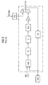
- Fig. 1 shows a not accessible node in the signal path which is driven by an analogue amplifier.
- Figure 2 To test such a not accessible node a design for test solution according to the state of the art is shown in Figure 2.
- a multiplexor For access to the node a multiplexor is provided so that a test signal can be applied directly to the node (e.g. from an external signal generator).
- the multiplexor is controlled by a mode control signal which switches between a test signal T and the amplified normal signals S of the signal path. All signals are differential signals.
- the drawback of a multiplexor-based solution is that the load capacitance is increased. Further providing a multiplexor increases the necessary area on the chip such increasing production costs. A further drawback is that because of the additional multiplexor the power consumption is increased.
- the invention provides an analogue amplifier with multiplexing capability comprising:
- the basic idea of the present invention is that in the main signal propagation path of analogue integrated circuits a number of amplifiers are provided to drive proper internal nodes in order and to guarantee the required signal to noise ratio. Whenever a controllability issue is detected the design of some amplifier is modified to include multiplexing capabilities that allow injecting test signals within the main signal propagation path with minimal redesign effort and minimal impact upon normal operation mode of the required amplification function.
- the amplifying transistor has a first terminal switched to said signal input in the normal amplifying mode, a second terminal which is connected to an output port of that amplifier and to a load device which is switched to a first supply voltage (VDD) in said normal amplifying mode, and and a third terminal connected to a tail current sink.
- VDD first supply voltage
- the tail current sink comprises a transistor with a first terminal switched to a bias voltage in said normal amplifying mode and to a second supply voltage (V ss ) in said test mode.
- the load device connected to the amplifying transistor is switched to the test input in said test mode.
- the amplifier is in a preferred embodiment a fully differential amplifier.
- the test signal is generated in a first embodiment by a built in test pattern generator.
- test signal is applied in an alternative embodiment via a pad from an external test pattern generator.
- FIG. 3 shows a conventional approach for testing a phase locked loop, (pLL), circuit within mixed signal circuits.
- a phase locked loop is a system with induced feedback to maintain an output signal in a specific phase relationship with a reference signal.
- the pll-circuit shown in figure 3 comprises of phase frequency detector PFD controlling a charge pump CP which supplies a deviation signal to the low pass filter LP.
- the filtered signal is supplied to a voltage controlled oscillator VCO.
- the voltage controlled oscillator VCO is a circuit that produces an AC-output signal whose frequency is proportional to the input control voltage.
- the VCO output signal is amplified by a conventional amplifier as shown in figure 4.
- a multiplexor is provided at the output of the amplifier in the conventional approach as shown in figure 3.
- a division circuit In the feedback loop a division circuit is provided which produces an output signal whose frequency is an integer division of the input signal frequency.
- the VCO signal is fed back within the pLL-circuit through a high speed 1/N frequency divider. The proper operation of these frequency divider is essential to guarantee a good pLL-performance.
- Figure 4 shows a conventional state of the art differential amplifier A.
- the amplifier A is connected to a biasing circuit.
- the conventional amplifier A as shown in figure 4 comprises two input terminals and two output terminals.
- the input terminals are connected to the gate terminals of amplifying MOS-transistors T a .
- the source nodes of the amplifying transistors T a are connected at a common node to a tail current sink implemented by transistor T b having a gate which is biased by a reference voltage.
- the drain terminals of the amplifying transistors T a are connected via resistors to a positive supply voltage VDD.
- the design of the conventional amplifier A as drawn in figure 4 is modified to increase the controllability of an internal node driven by said amplifier.
- the testability of the circuit under test including said amplifier is increased too.
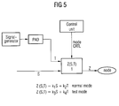
- FIG. 5 shows a block diagram of an analogue amplifier 1 according to the present invention.
- the analogue amplifier 1 according to the present invention as shown in figure 5 can be switched via a control mode signal between a first normal amplifying mode and a second test mode.
- a control mode signal is used to switch between both modes.
- the signal generator can be located externally or be built in.
- K 2 of the analogue amplifier 1 according to the present invention is as small as possible (K 2 ⁇ 0).
- the constant K 3 is zero to isolate the signal S of the signal path from the injected test signal T.
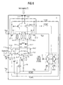
- Figure 6 shows a circuit diagram of a preferred embodiment of a differential analogue amplifier 1 according to the present invention.
- the analogue amplifier 1 is fully differential.
- the differential analogue amplifier 1 comprises an input port 2-1, 2-2 for receiving an analogue signal S.
- the amplifier 1 further comprises a test input port 3-1, 3-2 for receiving a test signal T.
- a control input port 4 is provided for receiving a test control signal switching the amplifier 1 between a normal amplifying mode and a test mode.
- the normal amplifying mode the amplifier 1 as shown in figure 6 amplifies the analogue signal S and transmits the amplified signal via an output port 5-1, 5-2 to an internal node within the integrated circuit.
- the test signal T is transmitted to that internal node.
- the amplifier 1 comprises an amplifying transistor 6-1, 6-2 having a gate terminal 7-1, 7-2, a source terminal 8-1, 8-2 and a drain terminal 9-1, 9-2.
- the gate terminals 7-1, 7-2 of the amplifying transistors 6-1, 6-2 are connected via lines 10-1, 10-2 and first switches 11-1, 11-2 to the signal input terminals 2-1, 2-2.
- the drain terminals 9-1, 9-2 of the amplifying transistors 6-1, 6-2 are connected via lines 13-1, 13-2 to the output port 5-1, 5-2 of the amplifier 1. Connected to lines 13-1, 13-2 are resistors 14-1, 14-2.
- the source terminals 8-1, 8-2 of the amplifying transistors 6-1, 6-2 are connected via a line 15 to a drain terminal 16 of a tail current sink comprising a transistor 17 having a source terminal 18 connected to a second negative supply voltage V ss .
- the current tail transistor 17 comprises a gate 20 connected via a line 21 and via a second switch 22 to a biasing reference voltage supplied to a terminal 23 of the amplifier 1. Line 21 further connects gate 20 of current tail transistor 17 to a drain terminal of a switching transistor 24.
- the gate 20 of the tail current transistor 17 can be switched by the third switch 24 to the negative supply voltage V ss .
- the load devices 14-1, 14-2 connected to the amplifying transistor 6-1, 6-2 are connected via lines 26-1, 26-2 and fourth switches 27-1, 27-2 to a positive supply voltage.
- the load devices 14-1, 14-2 a further connected via fifth switches 28-1, 28-2 to the test signal input port. All switches 11-1, 11-2, 22, 24, 27-1, 27-2, 28-1, 28-2 of the amplifier 1 are controlled by a test control mode signal applied to the amplifier by terminal 4.
- Two inverter circuits 29-1, 29-2 invert the test control mode signal, wherein the inverter circuit 29-1 supplies the signal not (T-CTRL) to switches 28-1, 28-2, and to switch 22, and wherein inverter circuit 29-2 supplies the signal T-CTRL to switches 11-1, 11-2, switch 24 and switches 27-1 and 27-2.
- switch 24 and switch 28-1, 28-2 are switched off and switches 27-1, 27-2, 11-1, 11-2, 22 are switched on.
- the test signal is cut off from the output terminal 5 of the amplifier 1.
- the gate 7-1, 7-2 of the amplifying transistor 6-1, 6-2 receives the analogue signal via a switch 11-11, 11-2 and transmits the amplified signals to output port 5-1, 5-2 of the amplifier 1.
- the gate 20 of the tail current transistor 17 receives the biasing reference voltage via closed switch 22. Since switch 27 is also closed in the normal amplifying mode the amplifying transistor 6 receives the positive supply voltage V DD via the loading resistors 14-1, 14-2.
- switches 28-1 and 28-2, and switch 24 are closed.
- switches 27-1, 27-2, 11-1, 11-2 and 22 are opened.
- While switching off switch 27 the amplifying transistor 6 is disconnected from the positive supply voltage V DD and cut off.
- By opening switch 11-1, 11-2 no input signal is supplied to the gate 7-1, 7-2 of the amplifying transistor 6-1, 6-2.
- the transistor 17 By switching off switch 22 the transistor 17 does not get a biasing reference voltage. Furthermore its gate 20 is switched to the negative supply voltage V ss by closing switch 24. In this manner the transistor 17 is cut off completely and the tail current going to ground is nullified.
- the amplifier design as shown in figure 6 focus on the tail current sink and loads of the amplifier 1 which are modified by the switches to reconfigure the operation of the amplifier.
- the design of a conventional amplifier is modified by adding switches that disconnect the amplifying transistor from the incoming signal and the tail current sink transistor from the bias circuitry. The design is modified in such a way that the injection of the test signal T in the signal path has a minimal impact upon the circuit normal operation.
- Figures 7-12 come from simulation analysis carried out at the operational frequency of 1.6 GHz.
- Figure 7a, 7b show the differential output wave forms of an original differential amplifier as shown in figure 4 in comparison to the differential output of the amplifier 1 according to the present invention as shown in figure 6.
- the input signal used is a monotonic sinusoidal at 1,562 GHz.
- Figure 8 shows the spectral content of the output voltages of the conventional amplifier (a) shown in figure 4 and the amplifier (b) according to the present invention as shown in figure 6.
- the increase of the noise figure at the operation frequency is due mainly to the drop in conversion gain related to the attenuation effect of transistors 11-1 and 11-2.
- the second largest contribution to the relative increase in the noise figure at the operation frequency is coming from transistor switches 27-1, 27-2 accounting to less than a quarter of the contribution of transistor switches 11-1, 11-2.
- Figure 9 shows the plot of noise figures with a measurement mark at a operating frequency (conventional amplifier a; amplifier according to the present invention b).
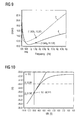
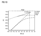
- Figures 10 to 13 show different plots of measuring intermodulation distortion products.
- the performance of the amplifier according to the present invention it is about 1,5 to 2 dBm better than the original amplifier according to the state of the art.
- Parasitic capacitance to ground together with the on resistance in transistors 11-1, 11-2 implement a low past filter at the inputs 2-1, 2-2 of the differential amplifier in the modified circuit.
- the attenuation provided by this filter at the operating frequency which accounts for the gain drop depicted in figure 7 is also responsible for the improvement observed in the circuit linearity. Since the filter attenuation reduces the input power to the differential amplifier it behaves better in terms of intermodulation distortion.
- Area overhead due to the amplifier design according to the invention accounts for about 9% of the original area due to the original amplifier design. This figure expressed in terms of a total pLL-area, where the amplifier is located, represents about only 0.023% since the amplifier itself takes only about 0.25% of the total pLL-area.
- a low impedance propagation path exist between the test port 3-1, 3-2 and the corresponding circuit output nodes 5-1, 5-2, respectively.
- Transistors 28-1, 28-2 used to disconnect the test ports 3-1, 3-2 are dimensioned according to the impedance requirements. These elements are placed in series with the loading resistors.
- a device under test can be reconfigured and its outputs multiplexed to inject test signals. Consequently it is possible to increase the controllability of relevant nodes of the circuit under test, and therefore is testability is also enhanced.
- the present invention can be adapted to different operating frequencies, ranging from DC to frequencies in the order of tens of GHZ typically used in optical communication circuits.
- the present invention is applicable to any analogue circuit whose controllability is to be increased.
- the modification of the design of a conventional amplifier makes possible to inject a test signal (T) with a minimum impact upon the circuit performances. Further the area overhead due to the circuit modification remains below 10% of that of the differential amplifier.
Landscapes
- Engineering & Computer Science (AREA)
- Architecture (AREA)
- Mechanical Engineering (AREA)
- Civil Engineering (AREA)
- Structural Engineering (AREA)
- Power Engineering (AREA)
- Amplifiers (AREA)
- Tests Of Electronic Circuits (AREA)
Abstract
Description
- The invention refers to an analogue amplifier to increase circuit testability by featuring additional multiplexing capability.
- Any procedure carried out upon an integrated circuit intended to establish its quality, performance or reliability is commonly called testing.
- Testing can be carried out at different stages during the development of an integrated circuit; different procedures are followed, according to particular goals and circuit type, for each development stage.
- The degree to which an integrated circuit facilitates the establishment of test criteria and the performance of tests to determine whether those criteria have been met is commonly referred as testability.
- According to existing literature, integrated circuits testability can be quantified by means of existing capacity to control and or to observe voltages on relevant nodes in the integrated circuit. These magnitudes are commonly referred as controllability and observability.
- The twin requirements of high precision and accuracy in signal measurement are superimposed to those basic requirements of controllability and observability to establish proper test criteria for modern high-speed communication circuits. On the other hand, new technologies make more and more defects to be non-visible, new failure mechanisms emerge and a relevant number of circuit features are unsimulatable.
- As a consequence, test cost and complexity increases, but also a higher risk exist to produce delays in bringing products to market or just to suffer from yield detractors that lead to higher manufacturing cost.
- Setting up design procedures that include some constrains to increase circuit testability is a common approach to address that problem.
- Testability can be improved either by increasing the controllability or the observability of some internal nodes. Identifying a testability issue, and therefore choosing proper nodes upon which to act in order to improve their observability or their controllability is most of the times an ad hoc issue.
- Conventional approach to raise up internal nodes controllability or observability uses multiplexors to provide alternative signal paths. However, because of the ad-hoc nature of the task, top level floor plan layout constrains may lead to situations where it is not possible to include new multiplexor blocks in the original design without severe impact upon schedule because of the re-design effort due.
- Fig. 1 shows a not accessible node in the signal path which is driven by an analogue amplifier. To test such a not accessible node a design for test solution according to the state of the art is shown in Figure 2. For access to the node a multiplexor is provided so that a test signal can be applied directly to the node (e.g. from an external signal generator). The multiplexor is controlled by a mode control signal which switches between a test signal T and the amplified normal signals S of the signal path. All signals are differential signals.
- The drawback of a multiplexor-based solution is that the load capacitance is increased. Further providing a multiplexor increases the necessary area on the chip such increasing production costs. A further drawback is that because of the additional multiplexor the power consumption is increased.
- Accordingly it is the object of the present invention to provide means which allow a better testability by increasing internal controllability.
This object is achieved by an analogue amplifier having the features of main claim 1. - Further advantages of the present invention are that the re-design effort is minimal, that the silicon area overhead is minimal and that the increase of the power supply current consumption is minimal.
- The invention provides an analogue amplifier with multiplexing capability comprising:
- an input port for receiving an analogue signal (S),
- a test input port for receiving a test signal (T),
- an output port for transmitting an analogue signal (0),
- a control input for receiving a test control signal (CRTL-mode) switching the amplifier between a normal amplifying mode and a test mode, wherein in the normal amplifying mode the analogue signal in the input port (S) is amplified to the output port (0),
-
- The basic idea of the present invention is that in the main signal propagation path of analogue integrated circuits a number of amplifiers are provided to drive proper internal nodes in order and to guarantee the required signal to noise ratio. Whenever a controllability issue is detected the design of some amplifier is modified to include multiplexing capabilities that allow injecting test signals within the main signal propagation path with minimal redesign effort and minimal impact upon normal operation mode of the required amplification function.
- In a preferred embodiment of the analogue amplifier according to the present invention the amplifying transistor has
a first terminal switched to said signal input in the normal amplifying mode,
a second terminal which is connected to an output port of that amplifier and to a load device which is switched to a first supply voltage (VDD) in said normal amplifying mode, and
and a third terminal connected to a tail current sink. - In a preferred embodiment of the analogue amplifier according to the present invention the tail current sink comprises a transistor with
a first terminal switched to a bias voltage in said normal amplifying mode and to
a second supply voltage (Vss) in said test mode. - In a preferred embodiment of the analogue amplifier according to the present invention the load device connected to the amplifying transistor is switched to the test input in said test mode.
- The amplifier is in a preferred embodiment a fully differential amplifier.
- The test signal is generated in a first embodiment by a built in test pattern generator.
- The test signal is applied in an alternative embodiment via a pad from an external test pattern generator.
- In the following preferred embodiments of the analogue amplifier according to the present invention are described with reference to the enclosed figures.
- Figure 1 shows the signal path in an analogue circuit according to the state of the art;
- Figure 2 shows a conventional approach to increase the controllability of an internal node non accessible from any primary input/output of the circuit under test.
- Figure 3 shows a pll circuit with added multiplexor according to the state of the art to increase controllability by bypassing the amplified VCO output.
- Figure 4 shows a fully differential amplifier, tail current and bias generation according to the state of the art;
- Figure 5 shows an arrangement comprising an amplifier according to the present invention in order to increase the controllability of the circuit node driven by said amplifier;
- Figure 6 shows a preferred embodiment of the analogue amplifier according to the present invention;
- Figure 7b shows a differential output voltage from an amplifier according to the state of the art as shown in figure 4 and figure 7a shows a differential output voltage from an ADfT-analogue amplifier according to the present invention as shown in figure 6;
- Figure 8 shows the spectral content of the output voltages of a conventional amplifier and of the analogue amplifier according to the present invention;
- Figure 9 shows noise figure curves of a conventional amplifier and of the analogue amplifier according to the present invention;
- Figure 10 shows the 1 dB compression point of the conventional amplifier according to the state of the art;
- Figure 11 shows the 1 dB compression point of the analogue amplifier according to the present invention;
- Figure 12 shows the IP3 (3rd order intersection point) for the conventional amplifier;
- Figure 13 shows the IP3 for the amplifier according to the present invention.
-
- Figure 3 shows a conventional approach for testing a phase locked loop, (pLL), circuit within mixed signal circuits. A phase locked loop is a system with induced feedback to maintain an output signal in a specific phase relationship with a reference signal. The pll-circuit shown in figure 3 comprises of phase frequency detector PFD controlling a charge pump CP which supplies a deviation signal to the low pass filter LP. The filtered signal is supplied to a voltage controlled oscillator VCO. The voltage controlled oscillator VCO is a circuit that produces an AC-output signal whose frequency is proportional to the input control voltage. The VCO output signal is amplified by a conventional amplifier as shown in figure 4. For test purposes a multiplexor is provided at the output of the amplifier in the conventional approach as shown in figure 3. In the feedback loop a division circuit is provided which produces an output signal whose frequency is an integer division of the input signal frequency. The VCO signal is fed back within the pLL-circuit through a high speed 1/N frequency divider. The proper operation of these frequency divider is essential to guarantee a good pLL-performance.
- By providing a multiplexor to the output of amplifier A the load capacitance, the area overhead and the power supply consumption are increased.
- Figure 4 shows a conventional state of the art differential amplifier A. The amplifier A is connected to a biasing circuit. The conventional amplifier A as shown in figure 4 comprises two input terminals and two output terminals. The input terminals are connected to the gate terminals of amplifying MOS-transistors Ta. The source nodes of the amplifying transistors Ta are connected at a common node to a tail current sink implemented by transistor Tb having a gate which is biased by a reference voltage. The drain terminals of the amplifying transistors Ta are connected via resistors to a positive supply voltage VDD.
- According to the present invention the design of the conventional amplifier A as drawn in figure 4 is modified to increase the controllability of an internal node driven by said amplifier. Thus the testability of the circuit under test including said amplifier is increased too.
- Figure 5 shows a block diagram of an analogue amplifier 1 according to the present invention. The analogue amplifier 1 according to the present invention as shown in figure 5 can be switched via a control mode signal between a first normal amplifying mode and a second test mode. A control mode signal is used to switch between both modes. The signal generator can be located externally or be built in.
- The function of the amplifier 1 in the normal mode can be described as:
T is the test signal and
K1, K2 are constants. - Since the function of the conventional amplifier to be modified can be described as:
- In the normal test node the constant K2 of the analogue amplifier 1 according to the present invention is as small as possible (K2 → 0).
- When the analogue amplifier 1 according to the present invention is switched to the test mode its operation can be described as:
- In an ideal implementation of the differential amplifier 1 according to the present invention, the constant K3 is zero to isolate the signal S of the signal path from the injected test signal T. The constant K4 is close to or lower than one in an ideal implementation (K3 = 0; K4 ≤ 1).
- Figure 6 shows a circuit diagram of a preferred embodiment of a differential analogue amplifier 1 according to the present invention. The analogue amplifier 1 is fully differential.
- The differential analogue amplifier 1 comprises an input port 2-1, 2-2 for receiving an analogue signal S. The amplifier 1 further comprises a test input port 3-1, 3-2 for receiving a test signal T. Further a control input port 4 is provided for receiving a test control signal switching the amplifier 1 between a normal amplifying mode and a test mode. In the normal amplifying mode the amplifier 1 as shown in figure 6 amplifies the analogue signal S and transmits the amplified signal via an output port 5-1, 5-2 to an internal node within the integrated circuit. In the test mode the test signal T is transmitted to that internal node.
- The amplifier 1 comprises an amplifying transistor 6-1, 6-2 having a gate terminal 7-1, 7-2, a source terminal 8-1, 8-2 and a drain terminal 9-1, 9-2. The gate terminals 7-1, 7-2 of the amplifying transistors 6-1, 6-2 are connected via lines 10-1, 10-2 and first switches 11-1, 11-2 to the signal input terminals 2-1, 2-2.
- The drain terminals 9-1, 9-2 of the amplifying transistors 6-1, 6-2 are connected via lines 13-1, 13-2 to the output port 5-1, 5-2 of the amplifier 1. Connected to lines 13-1, 13-2 are resistors 14-1, 14-2. The source terminals 8-1, 8-2 of the amplifying transistors 6-1, 6-2 are connected via a line 15 to a drain terminal 16 of a tail current sink comprising a transistor 17 having a source terminal 18 connected to a second negative supply voltage Vss. The current tail transistor 17 comprises a gate 20 connected via a line 21 and via a second switch 22 to a biasing reference voltage supplied to a terminal 23 of the amplifier 1. Line 21 further connects gate 20 of current tail transistor 17 to a drain terminal of a switching transistor 24.The gate 20 of the tail current transistor 17 can be switched by the third switch 24 to the negative supply voltage Vss.
- The load devices 14-1, 14-2 connected to the amplifying transistor 6-1, 6-2 are connected via lines 26-1, 26-2 and fourth switches 27-1, 27-2 to a positive supply voltage. The load devices 14-1, 14-2 a further connected via fifth switches 28-1, 28-2 to the test signal input port.
All switches 11-1, 11-2, 22, 24, 27-1, 27-2, 28-1, 28-2 of the amplifier 1 are controlled by a test control mode signal applied to the amplifier by terminal 4. Two inverter circuits 29-1, 29-2 invert the test control mode signal, wherein the inverter circuit 29-1 supplies the signal not (T-CTRL) to switches 28-1, 28-2, and to switch 22, and wherein inverter circuit 29-2 supplies the signal T-CTRL to switches 11-1, 11-2, switch 24 and switches 27-1 and 27-2. - The following table shows the states of the switches within the amplifier 1 drawn in figure 6 according to the present invention.
switch test mode normal mode S28-1, S28-2 On Off S27-1, S27-2 Off On S11-1, S11-2 Off On S22 Off On S24 On off - In the normal amplifying mode switch 24 and switch 28-1, 28-2 are switched off and switches 27-1, 27-2, 11-1, 11-2, 22 are switched on. By means of the switch 28-1, 28-2 the test signal is cut off from the output terminal 5 of the amplifier 1. The gate 7-1, 7-2 of the amplifying transistor 6-1, 6-2 receives the analogue signal via a switch 11-11, 11-2 and transmits the amplified signals to output port 5-1, 5-2 of the amplifier 1. In the normal amplifying mode the gate 20 of the tail current transistor 17 receives the biasing reference voltage via closed switch 22. Since switch 27 is also closed in the normal amplifying mode the amplifying transistor 6 receives the positive supply voltage VDD via the loading resistors 14-1, 14-2.
- When switched to the test mode switches 28-1 and 28-2, and switch 24 are closed. At the same time switches 27-1, 27-2, 11-1, 11-2 and 22 are opened. While switching off switch 27 the amplifying transistor 6 is disconnected from the positive supply voltage VDD and cut off. By opening switch 11-1, 11-2 no input signal is supplied to the gate 7-1, 7-2 of the amplifying transistor 6-1, 6-2. By isolating gates of the amplifying transistors 6-1, 6-2 from the input signal via switches 11-1, 11-2 the signal S is isolated from the output port 5-1, 5-2.. This ensures that the test signal T supplied to the output port 5-1, 5-2 via the load resistors 14-1, 14-2 is not affected by spurious signals coming from the input terminals 2-1, 2-2.
- By switching off switch 22 the transistor 17 does not get a biasing reference voltage. Furthermore its gate 20 is switched to the negative supply voltage Vss by closing switch 24. In this manner the transistor 17 is cut off completely and the tail current going to ground is nullified. The amplifier design as shown in figure 6 focus on the tail current sink and loads of the amplifier 1 which are modified by the switches to reconfigure the operation of the amplifier. The design of a conventional amplifier is modified by adding switches that disconnect the amplifying transistor from the incoming signal and the tail current sink transistor from the bias circuitry. The design is modified in such a way that the injection of the test signal T in the signal path has a minimal impact upon the circuit normal operation.
- Figures 7-12 come from simulation analysis carried out at the operational frequency of 1.6 GHz.
- Figure 7a, 7b show the differential output wave forms of an original differential amplifier as shown in figure 4 in comparison to the differential output of the amplifier 1 according to the present invention as shown in figure 6. The input signal used is a monotonic sinusoidal at 1,562 GHz.
- Figure 8 shows the spectral content of the output voltages of the conventional amplifier (a) shown in figure 4 and the amplifier (b) according to the present invention as shown in figure 6.
- The increase of the noise figure at the operation frequency is due mainly to the drop in conversion gain related to the attenuation effect of transistors 11-1 and 11-2. The second largest contribution to the relative increase in the noise figure at the operation frequency is coming from transistor switches 27-1, 27-2 accounting to less than a quarter of the contribution of transistor switches 11-1, 11-2.
- Figure 9 shows the plot of noise figures with a measurement mark at a operating frequency (conventional amplifier a; amplifier according to the present invention b).
- Figures 10 to 13 show different plots of measuring intermodulation distortion products. The performance of the amplifier according to the present invention it is about 1,5 to 2 dBm better than the original amplifier according to the state of the art.
- Parasitic capacitance to ground together with the on resistance in transistors 11-1, 11-2 implement a low past filter at the inputs 2-1, 2-2 of the differential amplifier in the modified circuit. The attenuation provided by this filter at the operating frequency which accounts for the gain drop depicted in figure 7 is also responsible for the improvement observed in the circuit linearity. Since the filter attenuation reduces the input power to the differential amplifier it behaves better in terms of intermodulation distortion.
- Area overhead due to the amplifier design according to the invention accounts for about 9% of the original area due to the original amplifier design. This figure expressed in terms of a total pLL-area, where the amplifier is located, represents about only 0.023% since the amplifier itself takes only about 0.25% of the total pLL-area. In the test mode a low impedance propagation path exist between the test port 3-1, 3-2 and the corresponding circuit output nodes 5-1, 5-2, respectively.
- Transistors 28-1, 28-2 used to disconnect the test ports 3-1, 3-2 are dimensioned according to the impedance requirements. These elements are placed in series with the loading resistors.
- According to the present invention a device under test can be reconfigured and its outputs multiplexed to inject test signals. Consequently it is possible to increase the controllability of relevant nodes of the circuit under test, and therefore is testability is also enhanced.
- The present invention can be adapted to different operating frequencies, ranging from DC to frequencies in the order of tens of GHZ typically used in optical communication circuits. The present invention is applicable to any analogue circuit whose controllability is to be increased.
- The modification of the design of a conventional amplifier makes possible to inject a test signal (T) with a minimum impact upon the circuit performances. Further the area overhead due to the circuit modification remains below 10% of that of the differential amplifier.
-
- 1
- analogue amplifier
- 2-1, 2-2
- input terminal
- 3-1, 2-2
- test input terminal
- 4
- test control input port
- 5-1, 5-2
- output port
- 6-1, 6-2
- amplifying transistors
- 7-1, 7-2
- gate terminals
- 8-1, 8-2
- source terminals
- 9-1, 9-2
- drain terminals
- 10-1, 10-2
- lines
- 11-1, 11-2
- first switches
- 13-1, 13-2
- lines
- 14-1, 14-2
- load devices
- 15
- line
- 16
- drain terminal
- 17
- current tail transistor
- 18
- source terminal
- 20
- gate
- 21
- line
- 22
- second switch
- 23
- terminal
- 24
- third switch
- 26-1, 26-2
- lines
- 27-1, 27-2
- fourth switches
- 28-1, 28-2
- fifth switches
- 29-1, 29-2
- inverter circuits
wherein in the test mode the test signal (T) is routed to said output port (0).
Claims (7)
- Analogue amplifier with multiplexing capability comprising:(a) an input port (2) for receiving an analogue signal (S);(b) a test input port (3) for receiving a test signal (T);(c) an output port (5);(d) a control input (4) for receiving a test control signal (CRTL-mode) switching the amplifier (1) between a normal amplifying mode and a test mode;(e) wherein in the normal amplifying mode the analogue signal (S) is amplified and transmitted via said output port (5);(f) wherein in the test mode the test signal (T) is routed to said output port (5).
- Analogue amplifier according to claim 1, wherein an amplifying transistor (6) is provided, having:a first terminal (7) switched to the said signal input (2) in the normal amplifying mode,a second terminal (9) which is connected to the output port (5) of the said amplifier (1) and to a load device (14) which is switched to a first supply voltage (VDD) in said normal amplifying mode, anda third terminal (8) connected to a tail current sink.
- Analogue amplifier according to claim 2 wherein the tail current sink comprises a transistor (17) with:a first terminal (20) switched to a bias voltage in said normal amplifying mode and to a second supply voltage (Vss) in said test mode.
- Analogue amplifier according to claim 2 wherein the load device (14) connected to the amplifying transistor (6) is switched to the test input (3) in the said test mode.
- Analogue amplifier according to claim 1 wherein the amplifier is a fully differential amplifier.
- Analogue amplifier according to claim 1 wherein the test signal is generated by a built in test pattern generator.
- Analogue amplifier according to claim 1 wherein the test signal is applied via a pad from an external test pattern generator.
Priority Applications (5)
| Application Number | Priority Date | Filing Date | Title |
|---|---|---|---|
| EP03001327A EP1441439A1 (en) | 2003-01-23 | 2003-01-23 | Analogue amplifier with multiplexing capability |
| TW092134105A TWI282212B (en) | 2003-01-23 | 2003-12-03 | Analogue amplifier with multiplexing capability |
| CNB2003101205674A CN1271782C (en) | 2003-01-23 | 2003-12-12 | Analog amplifier having multiplex function |
| KR1020040003648A KR100604129B1 (en) | 2003-01-23 | 2004-01-19 | Analogue amplifier multiplexing capability |
| US10/762,960 US7026865B2 (en) | 2003-01-23 | 2004-01-21 | Analogue amplifier with multiplexing capability |
Applications Claiming Priority (1)
| Application Number | Priority Date | Filing Date | Title |
|---|---|---|---|
| EP03001327A EP1441439A1 (en) | 2003-01-23 | 2003-01-23 | Analogue amplifier with multiplexing capability |
Publications (1)
| Publication Number | Publication Date |
|---|---|
| EP1441439A1 true EP1441439A1 (en) | 2004-07-28 |
Family
ID=32524178
Family Applications (1)
| Application Number | Title | Priority Date | Filing Date |
|---|---|---|---|
| EP03001327A Withdrawn EP1441439A1 (en) | 2003-01-23 | 2003-01-23 | Analogue amplifier with multiplexing capability |
Country Status (5)
| Country | Link |
|---|---|
| US (1) | US7026865B2 (en) |
| EP (1) | EP1441439A1 (en) |
| KR (1) | KR100604129B1 (en) |
| CN (1) | CN1271782C (en) |
| TW (1) | TWI282212B (en) |
Families Citing this family (9)
| Publication number | Priority date | Publication date | Assignee | Title |
|---|---|---|---|---|
| JP4887640B2 (en) * | 2005-03-15 | 2012-02-29 | 日本電気株式会社 | Analog differential circuit test equipment |
| US7545834B1 (en) * | 2006-01-10 | 2009-06-09 | Pericom Semiconductor Corp. | Multiple channel switch using differential de-mux amplifier and differential mux equalizer |
| CN102137236B (en) * | 2010-01-25 | 2014-02-12 | 英属开曼群岛商恒景科技股份有限公司 | Image sensing system and relative amplification/digitization circuit thereof |
| CN102638232B (en) * | 2011-02-15 | 2015-07-15 | 三星半导体(中国)研究开发有限公司 | Port-reusable operational amplifier for microcontroller |
| CN102222028A (en) * | 2011-06-28 | 2011-10-19 | 北京电子工程总体研究所 | Signal interface adapter with display device |
| US8928408B2 (en) | 2013-01-24 | 2015-01-06 | Aeroflex Colorado Springs Inc. | High-gain low-noise preamplifier and associated amplification and common-mode control method |
| US10014899B2 (en) * | 2016-07-15 | 2018-07-03 | Texas Instruments Incorporated | System and method for built-in self-test of electronic circuits |
| CN106097850A (en) * | 2016-08-22 | 2016-11-09 | 中国电子科技集团公司第四十研究所 | The additional path loss compensating circuit of a kind of education experiment path and method |
| DE102023107250A1 (en) * | 2023-03-22 | 2024-09-26 | Elmos Semiconductor Se | Analog circuit with means for reconfiguration for a stress test and/or for an IDDQ test and associated methods |
Citations (4)
| Publication number | Priority date | Publication date | Assignee | Title |
|---|---|---|---|---|
| US4546327A (en) * | 1982-07-14 | 1985-10-08 | Tokyo Shibaura Denki Kabushiki Kaisha | Analog signal power amplifier circuit |
| EP0475118A2 (en) * | 1990-08-31 | 1992-03-18 | Fujitsu Limited | Current mirror amplifier circuit and method of driving the same |
| US5585763A (en) * | 1995-03-30 | 1996-12-17 | Crystal Semiconductor Corporation | Controlled impedance amplifier |
| US6107883A (en) * | 1998-09-10 | 2000-08-22 | Seiko Epson Corporation | High gain, high speed rail-to-rail amplifier |
Family Cites Families (6)
| Publication number | Priority date | Publication date | Assignee | Title |
|---|---|---|---|---|
| IT1214249B (en) * | 1987-06-10 | 1990-01-10 | Sgs Microelettronica Spa | HIGH PERFORMANCE CMOS OPERATIONAL AMPLIFIER. |
| US4896118A (en) * | 1988-10-26 | 1990-01-23 | Westinghouse Electric Corp. | Variable gain current-to-voltage amplifier with gain independent test mode operation |
| US5006812A (en) * | 1989-08-01 | 1991-04-09 | Rockwell International Corporation | Power amplifier with built-in test circuit |
| US5631602A (en) * | 1995-08-07 | 1997-05-20 | Delco Electronics Corporation | Wheatstone bridge amplifier circuit with integrated diagnostic testing |
| JPH09232883A (en) * | 1996-02-23 | 1997-09-05 | Oki Micro Design Miyazaki:Kk | Operational amplifier circuit |
| JP3611690B2 (en) * | 1996-10-14 | 2005-01-19 | 沖電気工業株式会社 | Semiconductor device |
-
2003
- 2003-01-23 EP EP03001327A patent/EP1441439A1/en not_active Withdrawn
- 2003-12-03 TW TW092134105A patent/TWI282212B/en not_active IP Right Cessation
- 2003-12-12 CN CNB2003101205674A patent/CN1271782C/en not_active Expired - Fee Related
-
2004
- 2004-01-19 KR KR1020040003648A patent/KR100604129B1/en not_active Expired - Lifetime
- 2004-01-21 US US10/762,960 patent/US7026865B2/en not_active Expired - Lifetime
Patent Citations (4)
| Publication number | Priority date | Publication date | Assignee | Title |
|---|---|---|---|---|
| US4546327A (en) * | 1982-07-14 | 1985-10-08 | Tokyo Shibaura Denki Kabushiki Kaisha | Analog signal power amplifier circuit |
| EP0475118A2 (en) * | 1990-08-31 | 1992-03-18 | Fujitsu Limited | Current mirror amplifier circuit and method of driving the same |
| US5585763A (en) * | 1995-03-30 | 1996-12-17 | Crystal Semiconductor Corporation | Controlled impedance amplifier |
| US6107883A (en) * | 1998-09-10 | 2000-08-22 | Seiko Epson Corporation | High gain, high speed rail-to-rail amplifier |
Also Published As
| Publication number | Publication date |
|---|---|
| TWI282212B (en) | 2007-06-01 |
| TW200414674A (en) | 2004-08-01 |
| CN1271782C (en) | 2006-08-23 |
| KR20040067953A (en) | 2004-07-30 |
| KR100604129B1 (en) | 2006-07-24 |
| US7026865B2 (en) | 2006-04-11 |
| CN1519577A (en) | 2004-08-11 |
| US20040150469A1 (en) | 2004-08-05 |
Similar Documents
| Publication | Publication Date | Title |
|---|---|---|
| US5584053A (en) | Commonly coupled high frequency transmitting/receiving switching module | |
| KR100352658B1 (en) | Integrated transceiver circuit packaged component | |
| US6859112B2 (en) | CMOS voltage controlled oscillator circuit for operation with low supply voltage and method for same | |
| Le et al. | A CMOS 77-GHz receiver front-end for automotive radar | |
| EP1441439A1 (en) | Analogue amplifier with multiplexing capability | |
| US7643847B2 (en) | Versatile baseband signal input current splitter | |
| US10263605B2 (en) | Frequency extender | |
| US20020101266A1 (en) | High bandwidth clock buffer | |
| US8761300B2 (en) | Peak detector with extended range | |
| US8301086B2 (en) | Low-power polar transmitter | |
| JPH09232882A (en) | Efficient rf cmos amplifier with increased mutual conductance | |
| US7227392B2 (en) | Frequency multiplier | |
| US6831521B1 (en) | Method and apparatus for detecting interruption of an input signal with cancellation of offset level | |
| US7873884B2 (en) | Wireless embedded test signal generation | |
| EP0160035A1 (en) | High efficiency igfet operational amplifier. | |
| Phan et al. | A 10.8-14.5 GHz 8-phase 12.5%-duty-cycle non-overlapping LO generator with automatic phase-and-duty-cycle calibration for 60-GHz 8-path-filtering sub-sampling receivers | |
| US20050077962A1 (en) | Interface circuit for connecting to an output of a frequency converter | |
| Onabajo et al. | An on-chip loopback block for RF transceiver built-in test | |
| Hafele et al. | A GaAs PHEMT distributed amplifier with low group delay time variation for 40 Gbit/s optical systems | |
| Fischer et al. | A 77-GHz SiGe frequency multiplier (× 18) for radar transceivers | |
| US20080143442A1 (en) | Electrical Circuit | |
| GB2078038A (en) | Superheterodyne receivers | |
| JPH04323907A (en) | Low-offset, high-speed cmos amplifier which separates noise in supplied electric power | |
| Amamiya et al. | Low supply voltage operation of over-40-Gb/s digital ICs based on parallel-current-switching latch circuitry | |
| Messinger et al. | Divide-by-8 phase detector MMIC for PLL-based carrier recovery in E-band communication |
Legal Events
| Date | Code | Title | Description |
|---|---|---|---|
| PUAI | Public reference made under article 153(3) epc to a published international application that has entered the european phase |
Free format text: ORIGINAL CODE: 0009012 |
|
| AK | Designated contracting states |
Kind code of ref document: A1 Designated state(s): AT BE BG CH CY CZ DE DK EE ES FI FR GB GR HU IE IT LI LU MC NL PT SE SI SK TR |
|
| AX | Request for extension of the european patent |
Extension state: AL LT LV MK RO |
|
| 17P | Request for examination filed |
Effective date: 20040813 |
|
| AKX | Designation fees paid |
Designated state(s): DE FR GB |
|
| GRAP | Despatch of communication of intention to grant a patent |
Free format text: ORIGINAL CODE: EPIDOSNIGR1 |
|
| STAA | Information on the status of an ep patent application or granted ep patent |
Free format text: STATUS: THE APPLICATION IS DEEMED TO BE WITHDRAWN |
|
| 18D | Application deemed to be withdrawn |
Effective date: 20070913 |