EP1441438A1 - An adjustable offset differential amplifier - Google Patents
An adjustable offset differential amplifier Download PDFInfo
- Publication number
- EP1441438A1 EP1441438A1 EP03257915A EP03257915A EP1441438A1 EP 1441438 A1 EP1441438 A1 EP 1441438A1 EP 03257915 A EP03257915 A EP 03257915A EP 03257915 A EP03257915 A EP 03257915A EP 1441438 A1 EP1441438 A1 EP 1441438A1
- Authority
- EP
- European Patent Office
- Prior art keywords
- differential
- sub
- transistor
- differential amplifier
- transistors
- Prior art date
- Legal status (The legal status is an assumption and is not a legal conclusion. Google has not performed a legal analysis and makes no representation as to the accuracy of the status listed.)
- Withdrawn
Links
- 230000005291 magnetic effect Effects 0.000 description 23
- 238000000034 method Methods 0.000 description 16
- 230000005415 magnetization Effects 0.000 description 13
- 238000012545 processing Methods 0.000 description 8
- 230000035945 sensitivity Effects 0.000 description 6
- 238000012360 testing method Methods 0.000 description 6
- 230000004888 barrier function Effects 0.000 description 3
- 230000001419 dependent effect Effects 0.000 description 3
- 238000004519 manufacturing process Methods 0.000 description 3
- 230000003071 parasitic effect Effects 0.000 description 3
- 239000000758 substrate Substances 0.000 description 3
- VYPSYNLAJGMNEJ-UHFFFAOYSA-N Silicium dioxide Chemical compound O=[Si]=O VYPSYNLAJGMNEJ-UHFFFAOYSA-N 0.000 description 2
- 238000012937 correction Methods 0.000 description 2
- 230000005641 tunneling Effects 0.000 description 2
- 229910052581 Si3N4 Inorganic materials 0.000 description 1
- 239000003990 capacitor Substances 0.000 description 1
- PMHQVHHXPFUNSP-UHFFFAOYSA-M copper(1+);methylsulfanylmethane;bromide Chemical compound Br[Cu].CSC PMHQVHHXPFUNSP-UHFFFAOYSA-M 0.000 description 1
- 238000013461 design Methods 0.000 description 1
- 238000001514 detection method Methods 0.000 description 1
- 239000003302 ferromagnetic material Substances 0.000 description 1
- 230000006870 function Effects 0.000 description 1
- 239000000395 magnesium oxide Substances 0.000 description 1
- CPLXHLVBOLITMK-UHFFFAOYSA-N magnesium oxide Inorganic materials [Mg]=O CPLXHLVBOLITMK-UHFFFAOYSA-N 0.000 description 1
- AXZKOIWUVFPNLO-UHFFFAOYSA-N magnesium;oxygen(2-) Chemical compound [O-2].[Mg+2] AXZKOIWUVFPNLO-UHFFFAOYSA-N 0.000 description 1
- TWNQGVIAIRXVLR-UHFFFAOYSA-N oxo(oxoalumanyloxy)alumane Chemical compound O=[Al]O[Al]=O TWNQGVIAIRXVLR-UHFFFAOYSA-N 0.000 description 1
- BPUBBGLMJRNUCC-UHFFFAOYSA-N oxygen(2-);tantalum(5+) Chemical compound [O-2].[O-2].[O-2].[O-2].[O-2].[Ta+5].[Ta+5] BPUBBGLMJRNUCC-UHFFFAOYSA-N 0.000 description 1
- 239000000377 silicon dioxide Substances 0.000 description 1
- 235000012239 silicon dioxide Nutrition 0.000 description 1
- HQVNEWCFYHHQES-UHFFFAOYSA-N silicon nitride Chemical compound N12[Si]34N5[Si]62N3[Si]51N64 HQVNEWCFYHHQES-UHFFFAOYSA-N 0.000 description 1
- 238000004088 simulation Methods 0.000 description 1
- 238000004513 sizing Methods 0.000 description 1
- 229910001936 tantalum oxide Inorganic materials 0.000 description 1
Images






Classifications
-
- G—PHYSICS
- G11—INFORMATION STORAGE
- G11C—STATIC STORES
- G11C7/00—Arrangements for writing information into, or reading information out from, a digital store
- G11C7/06—Sense amplifiers; Associated circuits, e.g. timing or triggering circuits
- G11C7/067—Single-ended amplifiers
-
- G—PHYSICS
- G11—INFORMATION STORAGE
- G11C—STATIC STORES
- G11C7/00—Arrangements for writing information into, or reading information out from, a digital store
- G11C7/06—Sense amplifiers; Associated circuits, e.g. timing or triggering circuits
- G11C7/08—Control thereof
-
- H—ELECTRICITY
- H03—ELECTRONIC CIRCUITRY
- H03F—AMPLIFIERS
- H03F3/00—Amplifiers with only discharge tubes or only semiconductor devices as amplifying elements
- H03F3/45—Differential amplifiers
- H03F3/45071—Differential amplifiers with semiconductor devices only
- H03F3/45479—Differential amplifiers with semiconductor devices only characterised by the way of common mode signal rejection
- H03F3/45632—Differential amplifiers with semiconductor devices only characterised by the way of common mode signal rejection in differential amplifiers with FET transistors as the active amplifying circuit
- H03F3/45744—Differential amplifiers with semiconductor devices only characterised by the way of common mode signal rejection in differential amplifiers with FET transistors as the active amplifying circuit by offset reduction
- H03F3/45766—Differential amplifiers with semiconductor devices only characterised by the way of common mode signal rejection in differential amplifiers with FET transistors as the active amplifying circuit by offset reduction by using balancing means
- H03F3/45771—Differential amplifiers with semiconductor devices only characterised by the way of common mode signal rejection in differential amplifiers with FET transistors as the active amplifying circuit by offset reduction by using balancing means using switching means
-
- H—ELECTRICITY
- H03—ELECTRONIC CIRCUITRY
- H03F—AMPLIFIERS
- H03F2203/00—Indexing scheme relating to amplifiers with only discharge tubes or only semiconductor devices as amplifying elements covered by H03F3/00
- H03F2203/45—Indexing scheme relating to differential amplifiers
- H03F2203/45212—Indexing scheme relating to differential amplifiers the differential amplifier being designed to have a reduced offset
-
- H—ELECTRICITY
- H03—ELECTRONIC CIRCUITRY
- H03F—AMPLIFIERS
- H03F2203/00—Indexing scheme relating to amplifiers with only discharge tubes or only semiconductor devices as amplifying elements covered by H03F3/00
- H03F2203/45—Indexing scheme relating to differential amplifiers
- H03F2203/45342—Indexing scheme relating to differential amplifiers the AAC comprising control means on a back gate of the AAC
-
- H—ELECTRICITY
- H03—ELECTRONIC CIRCUITRY
- H03F—AMPLIFIERS
- H03F2203/00—Indexing scheme relating to amplifiers with only discharge tubes or only semiconductor devices as amplifying elements covered by H03F3/00
- H03F2203/45—Indexing scheme relating to differential amplifiers
- H03F2203/45371—Indexing scheme relating to differential amplifiers the AAC comprising parallel coupled multiple transistors at their source and gate and drain or at their base and emitter and collector, e.g. in a cascode dif amp, only those forming the composite common source transistor or the composite common emitter transistor respectively
Definitions
- the invention relates generally to an amplifier. More particularly, the invention relates to an adjustable offset differential amplifier.
- differential amplifiers There are many uses for differential amplifiers. For example, differenrial amplifiers are commonly used within operational amplifiers, which are prevalent in electronics. Differential amplifiers can also be used to sense a logical state of memory cells within an array of memory cells.
- Offset errors of differential amplifiers can limit performance of the differential amplifier.
- differential amplifiers can be used to sense the resistance of a resistive memory cell. Offset errors of the differential amplifiers can hinder the reliability of the sensing of the resistive state of the resistive memory cells.
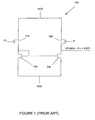
- Figure 1 shows a typical differential amplifier 100 that includes an offset error.
- the differential amplifier 100 can include a first input transistor 110, a second input transistor 120, a first output transistor 130 and a second output transistor 140.
- An output signal VO of the differential amplifier 100 is generally linearly related to a difference between a first input V+ and a second input V-.
- the output signal VO generally includes an offset error VOFF.
- Offset errors of differential amplifiers can be caused by physical design, or processing variations of the differential amplifiers. Circuit device thresholds, mismatches of device sizes, and circuit device operating conditions are all possible sources of offset errors. Physical size variations and process variations inherent in integrated circuit manufacturing processing are sources of offset errors. Processing errors are a major source of offset error in CMOS operations amplifiers that include differential amplifiers.
- a technique that has been used to minimize offset errors includes manipulating transistor sizing and physical circuit element layouts. Another technique includes the use of a switched capacitor circuit. Both of these technique require special manufacturing processing steps.
- the present invention seeks to provide an improved differential amplifier.
- an adjustable offset differential amplifier as specified in claim 1.
- a resistive cross-point memory cell sensor comprising:
- a resistive cross-point memory apparatus comprising:
- a resistive cross-point memory system comprising:
- a computer system comprising:
- the preferred embodiments can provide preferably the differential amplifier is adaptable for use within a sense amplifier of MRAM.
- a first embodiment of the invention includes an adjustable offset differential amplifier.
- the adjustable offset differential amplifier includes a first differential transistor receiving a first differential input, and a second differential transistor receiving a second differential input.
- a differential amplifier output includes a signal having an amplitude proportional to a difference between the first differential input and the second differential input.
- the first differential transistor includes a plurality of sub first differential transistors. Each sub first differential transistor includes an adjustable back gate bias. Control circuitry can be connected to the adjustable back gate bias of each of the sub first differential transistors for reducing offset errors of the differential amplifier output.
- the invention is embodied in an apparatus and method for reducing offset error associated with a differential amplifier.
- the preferred apparatus and method provide adjustment of the offset errors that is typically linear, and reduces the offset error with a positive or negative correction.
- the apparatus and method are robust and generally temperature insensitive.
- FIG. 2 shows an offset differential amplifier 200 including offset reduction circuitry according to an embodiment of the invention.
- the offset differential amplifier 200 includes a first differential transistor 210 receiving a first differential input (V+).
- a second differential transistor 220 receives a second differential input (V-).
- a differential amplifier output (OUTPUT) includes a signal that generally has a signal amplitude proportional to a difference between the first differential input (V+) and the second differential input (V-).
- the first differential transistor 210 can include a plurality of sub first differential transistors 212, 214, 216. Each sub first differential transistor 212, 214, 216 includes an adjustable back gate bias.
- Offset adjust control circuitry 250 can be connected to the adjustable back gate bias of each of the sub first differential transistors 212, 214, 216 for reducing offset errors of the differential amplifier output (OUTPUT).
- each of the sub first differential transistors 212, 214, 216 include physical dimension that are different than each of the other sub first differential transistors 212, 214, 216.
- An embodiment includes the sub first differential transistors 212, 214, 216 being configured so that the physical dimensions of the sub first differential transistors 212, 214, 216 are progressively larger. That is, each sub first differential transistors 212, 214, 216 is physically scaled to be a predetermined ratio larger than one other of the sub first differential transistors 212, 214, 216.
- the physical dimension of each sub first differential transistor 212, 214, 216 can be approximately twice the physical dimension of another sub first differential transistor 212, 214, 216.
- Another example includes the physical dimension of each sub first differential transistor 212, 214, 216 being approximately ten times the physical dimension of another sub first differential transistor 212, 214, 216.
- the back gate bias control of the sub first differential transistors 212, 214, 216 can be adjusted to minimize VOFF. Details of how the back gate bias control are adjusted will be discussed later.
- Figure 2 is merely an example of an embodiment of the invention.
- Other equivalent embodiments can include NMOS differential input transistors and PMOS output transistors.
- Other equivalent embodiments can include more or less than three sub first differential transistors.
- Figure 3 shows a substrate 300 that includes transistors that include a back gate bias adjust.
- the substrate 300 includes a PMOS 310 and an NMOS transistor 320, in which voltages applied to back gate control terminals (B) 312, 322 provide a back gate bias to each of the transistors 310, 320. Voltages applied to the back gate control terminals (B) can be biased to influence current flow through each of the transistors 310, 320.
- a voltage potential can be applied to the gates (G) 313, 323 of the transistors 310, 320 to cause charge to be collected in channels 314, 324 of the transistors 310, 320 causing the transistors 310, 320 to conduct current.
- the magnitude of the current conducted is generally dependent upon the magnitude of the voltage potential applied.
- a voltage potential can be applied to the back gates (B) 312, 322 (or bulk) of the transistors 310, 320 to additionally control the charge collected by the channel 314, 324 of the transistors 310, 320, which additionally controls the current conducted by the transistors 310, 320.
- PMOS 310 and NMOS transistors 320 have been disclosed because each of the embodiments of the invention can generally be implemented with either PMOS or NMOS transistors.
- the embodiments disclosed include N-well back gate bias transistors. It is to be understood that equivalent embodiments can include P-well back gate bias transistors.
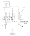
- Figure 4 shows a differential amplifier 400 including offset adjust control circuitry 450 according to another embodiment of the invention.
- a second differential transistor 420 of another embodiment includes an adjustable back gate bias. The back gate bias of the second differential transistor 420 provides for output offset adjustment in a direction that is opposite of the first differential transistor 210.
- the offset adjust control circuitry 450 includes additional circuitry for adjusting the back gate bias of the second differential transistor 420. Details of the offset adjust control circuitry 450 will be described later.
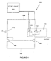
- FIG. 5 shows a differential amplifier 500 including offset adjust control circuitry 550 according to another embodiment of the invention.
- the adjustable offset differential amplifier of this embodiment includes a second differential transistor 520 that includes a plurality of sub second differential transistors 522, 524. Only two sub second differential transistors are included in this embodiment. However, clearly more sub second differential transistors can be included.
- Each sub second differential transistor 522, 524 includes an adjustable back gate bias for providing adjustment of the offset of the differential amplifier 500.
- the offset control circuitry 550 includes a connection to an adjustable back gate bias of each of the sub second differential transistors 522, 524 for reducing offset errors of the differential amplifier output (OUTPUT). Details of the offset adjust control circuitry 550 will be described later.
- Each of the sub second differential transistors 522, 524 can include physical dimension that are different than each of the other sub second differential transistors.
- the sub second differential transistors include progressively larger physical dimension sub second differential transistors.
- each progressively larger physical dimension sub second differential transistor can be approximately twice the physical dimension of a previous sub second differential transistor.
- Another example includes each progressively larger physical dimension sub second differential transistor being approximately ten times the physical dimension of a previous sub second differential transistor.
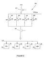
- Figure 6 shows a differential amplifier 600 including offset reduction control circuitry 650 according to another embodiment of the invention.
- the embodiment includes a first differential input transistor 610 that does not include a back gate bias control, and a second input differential transistor 520 that is the same as the second input differentia transistor 520 of Figure 5.
- Figure 7 shows physical dimensions of a sub differential amplifier transistors 722, 724, 726 of a differential input transistor 720 according to an embodiment of the invention.
- Physical dimensions of the sub differential amplifier transistors 722, 724, 726 are provided next to the sub differential amplifier transistors 722, 724, 726.
- the physical dimensions represent a width to length ratio of a channel of the corresponding transistor. For example, a channel width to length ratio of a first sub differential amplifier transistor 722 is 2/10.
- a channel width to length ratio of a second sub differential amplifier transistor 724 is 2/1.
- a channel width to length ratio of a third sub differential amplifier transistor 726 is 20/1.
- An offset adjustment sensitivity of the first sub differential amplifier transistor 722 can be designated as very fine.
- An offset adjustment sensitivity of the second sub differential amplifier transistor 724 can be designated as fine.
- An offset adjustment sensitivity of the third sub differential amplifier transistor 726 can be designated as coarse.
- the sensitivity of each sub differential amplifier transistor 722, 724, 726 is proportional to the channel width to length ratio of the sub differential amplifier transistor 722, 724, 726.
- An embodiment of the offset reduction control circuitry 750 includes very fine, fine and course back gate bias adjustments of the sub differential amplifier transistors 722, 724, 726.
- Figure 8 shows an offset adjust controller 800 according to an embodiment of the invention.
- the offset adjust controller 800 can be connected to a back gate bias of a single sub differential amplifier transistor. That is, for multiple sub differential amplifier transistors, an offset adjust controller 800 can be connected to a back gate of each of the multiple sub differential amplifier transistors.
- the offset adjust controller 800 of Figure 8 includes a programmable voltage divider for generating a back gate bias voltage for isolated wells of one of the sub differential amplifier transistors.
- the voltage divider is connected between a source of operating potential (VDD) and a reference potential (GND).
- the voltage divider is formed by upper and lower transistors 810, 820, and by four middle transistors 830, 840, 850, 860 having different drain-source path resistances. Turning on different combinations of the middle transistors 830, 840, 850, 860 changes the voltage drop between VDD and GND, thereby, setting the voltage potential of VBGbias. The voltage divider voltage drop is applied to a back gate of a corresponding sub differential amplifier transistor.
- the middle transistors 830, 840, 850, 860 are turned on and off according to a first number stored in a first group of latches 872, 874, 876, 878.
- the embodiment of Figure 8 includes the offset adjust controller 800 controlling the back gate bias voltage by as many as 2 4 different levels. Control lines S0, S1, S2, S3 determine which of the middle transistors 830, 840, 850, 860 are included within the voltage divider.
- the upper transistor 810 can be used to control the power to the back gate bias circuits.
- the lower transistor 820 can be used to select 1 of 2 or more back gate bias circuits.
- the back gate bias circuits can operate in pairs and share a common group of latch circuits 872, 874, 876, 878.
- a first back gate bias circuit can be used to adjust the offset in a first direction
- a second back gate bias circuit can be used to adjust the offset in a second (opposite) direction.
- the lower transistor 820 is off, the voltage potential of VBGbias is generally equal to the voltage potential of VDD.
- the lower transistor 820 When the lower transistor 820 is on, the voltage potential of VBGbias is generally set by the voltage divider.
- Figure 9 shows a resistive cross-point memory cell (RMEM) and a differential amplifier including offset reduction circuitry according to an embodiment of the invention.
- An operational amplifier 905 can include the previously described differential amplifiers 200, 400, 500.
- the resistive cross-point memory cell includes a resistance that is dependent upon a logical state stored within the resistive cross-point memory cell.
- An output SENSE can sense the logical state of the cross-point memory cell RMEM by applying a sense voltage and sensing a resulting current.
- a sense voltage VA is applied to a first input V+ of the operational amplifier 905.
- a resulting secondary sense voltage VA' is generated across the cross-point memory cell RMEM.
- the sense voltage is also applied by default across all of the other cross-point memory cells within an array of cross-point represented by RS.
- Sensing the resistive state of a single memory cell in an array of memory cells can be unreliable.
- all memory cells in the array are coupled together through many parallel paths.
- the resistance at one cross point is generally equal the resistance of the cross point in parallel with the resistance of memory cells of the other rows in columns (the array of memory cells can be characterized as a cross point resistor network). If the memory cell being sensed has a different resistance due to stored magnetization, a small difference voltage may develop. This small differential voltage can give rise to a parasitic or "sneak path" current.
- the parasitic current is typically larger than the sense current, and therefore, can obscure the sense current. Consequently, the parasitic current can prevent the resistance from being sensed.
- the sense voltage VA and the secondary sense voltage VA' are identical. Differences in the sense voltage VA and the secondary sense voltage VA' cause current ("sneak path" current) to flow through the non-selected resistive memory cells of an array of resistive memory cells.
- RS represents the resistance of the non-selected memory cells of the array of resistive memory cells. Current flowing through the non-selected memory cells cause errors in the current detected at the SENSE output due to the sense voltage VA, and therefore, introduce inaccuracies in the detection of the resistive state of the cross-point memory cell RMEM.
- Offset errors of differential amplifiers internal to the operational amplifier 905 cause the sense voltage VA and the secondary sense voltage VA' to deviate.
- the invention can be used to reduce the offset errors of the differential amplifiers within the operational amplifier 905. Therefore, the invention can be used to improve the performance of a resistive memory cell by reducing current flow through non-selected resistive memory cells.
- the following table provides actual simulated sensitivities of the very fine, fine and course back gate bias adjustments as shown in Figure 7, for the resistive cross-point memory cell (RMEM) and a differential amplifier including offset reduction circuitry of Figure 9.
- the differential amplifier simulation includes a supply voltage VDD of 3.3 V, a back gate voltage range of 3.2 to 3.3 V, a VA value of 0.5 V, an RMEM value of 1 Mega Ohm, and an RS value of 1 Kilo Ohm.
- RANGE SENSITIVITY RANGE MIN The differential amplifier simulation includes a supply voltage VDD of 3.3 V, a back gate voltage range of 3.2 to 3.3 V, a VA value of 0.5 V, an RMEM value of 1 Mega Ohm, and an RS value of 1 Kilo Ohm.
- the table depicts RANGE and MIN. STEP SIZE of the offset adjustment for the resistive cross-point memory cell and differential amplifier of Figure 9, with the sub differential amplifier transistors of Figure 7, and the offset controller of Figure 8.
- the coarse offset control has a range of 19.6 mV and a minimum offset control step size of 1.22 mV.
- the fine offset control has a range of 1.51 mV and a minimum offset control step size of 95 uV.
- the very fine offset control has a range of 170 uV and a minimum offset control step size of 1.1 uV.
- the state of the latches (for example, latches 872, 874, 876, 878 in Figure 8) in the back gate bias controller (for example, the offset adjust controller 800) is set during a calibration operation of the sense amplifier.
- the offset of the sense amplifier (differential amplifier) is varied until a test condition is met.
- the offset setting that meets the test condition is held by the back gate bias controller. That is, the offset setting state is held by the back gate controller latches (for example, latches 872, 874, 876, 878 in Figure 8).
- the test condition can include adjusting the sense amplifier offset until a target sense current equal to VA/RMEM is obtained. Once the target sense current has been obtained, the settings of the back gate controller latches are maintained.
- the time required to determined the optimal calibration can be minimized by including several ranges of calibration.
- the previously described coarse, fine and very fine ranges of calibration can be used to determine the optimal offset adjustment.
- the coarse calibration adjustment can be used to quickly limit the range of the calibration.
- the fine and very fine calibration adjustments can be used to determine the optimal calibration point.
- the size of the memory being sensed is limited by the precision of the offset adjustment control during calibration. Therefore, a robust very fine calibration allows proper sensing of a larger size memory array than otherwise would be possible.
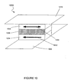
- Figure 10 shows an embodiment of a magnetic tunnel junction 1000 that can be used as a resistive memory cell.
- the magnetic tunnel junction 1000 includes a pinned layer 1034, a sense layer 1032 and a insulating tunnel barrier 1036.
- the pinned layer 1034 has a magnetization orientation that is fixed, and will not rotate in the presence of an applied magnetic field in a range of interest.
- the sense layer 1032 has a magnetization that can be oriented in either of two directions. A first magnetization orientation of the sense layer 1032 is in the same direction as the fixed magnetization of the pinned layer 1034. A second magnetization orientation of the sense layer 1032 is in the opposite direction as the fixed magnetization of the pinned layer 1034.
- a resistance across the magnetic tunnel junction 1000 will vary in magnitude depending upon the magnetic orientation of the sense layer 1032 with respect to the magnetic orientation of the pinned layer 1034. Typically, if the sense layer 1032 has a magnetic orientation that is in the opposite direction as the pinned layer 1034, then the resistance across the magnetic tunnel junction 1000 will be large. If the sense layer 1032 has a magnetic orientation that is in the same direction as the pinned layer 1034, then the resistance across the magnetic tunnel junction 1000 will be less.
- the resistive state of the magnetic tunnel junction is determined by comparing a sensed resistance with a predetermined resistive threshold value, and making a magnetic tunnel junction state determination based upon the comparision. That is, if the sensed resistance is iess than the predetermined threshold value, then the state of the magnetic tunnel junction is a first state. If the sensed resistance is greater than the predetermined threshold value, then the state of the magnetic tunnel junction is the second state.
- the orientation of the magnetic tunnel junction can be referred to as being "parallel.” If the magnetization of the sense layer and the reference layer of the magnetic tunnel junction are in opposite directions, the orientation of the magnetic tunnel junction can be referred to as being "anti-parallel.” The two orientations, parallel and anti-parallel, can correspond to magnetic tunnel junction states of low or high resistance.
- the insulating tunnel barrier 1036 allows quantum mechanical tunneling to occur between the reference layer 1034 and the sense layer 1032.
- the tunneling is electron spin dependent, causing the resistance of the magnetic tunnel junction 1000 to be a function of the relative orientations of the magnetization directions of the reference layer 1034 and the sense layer 1032.
- the presence of a magnetic field can be detected by establishing the magnetization orientation of the reference layer 1034 and the sense layer 1032.
- the resistance of the magnetic tunnel junction 1000 is a first value (R) if the magnetization orientation of the magnetic tunnel junction 1000 is parallel and a second value (R+delta) if the magnetization orientation is anti-parallel.
- the insulating tunnel barrier 1036 can be made of aluminum oxide, silicon dioxide, tantalum oxide, silicon nitride, aluminum nitride, or magnesium oxide.
- the sense layer 1032 may be made of a ferromagnetic material.
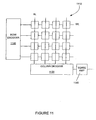
- Figure 11 shows an array of resistive cross point memory cells 1110 according to an embodiment of the invention.
- the cross-point memory array 1110 can be part of a cross-point memory system.
- Each resistive cross-point memory cell can include an MRAM memory cell.
- a row decoder 1120 and a column decoder 1130 select a memory cell.
- a logical state of the selected memory cell can be sensed by a sense amplifier 1140.
- Figure 12 shows a computing system 1200 that includes an array of resistive cross point memory cells according to an embodiment of the invention.
- the computing system 1200 includes a central processing unit 1210.
- the computing system 1200 further includes an array of cross-point memory cells 1230.
- the central processing unit 1210 can store and access data within the array of cross-point memory cells 1230.
- a row decoder 1260 and column decoder 1240 select a memory cell to be sensed.
- a plurality of resistive cross-point memory cell sensors 1250 can be electrically connected to each of the cross-point memory cells.
- Each resistive cross-point memory can include an MRAM memory cell.
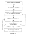
- Figure 13 shows steps included within a method reducing offset errors of a differential amplifier according to an embodiment of the invention.
- a first step 1310 includes a course calibration adjustment.
- a state of a coarse calibration register can be varied until a coarse calibration state satisfies a calibration test criteria (as previously described).
- the coarse adjustment can be initially set based upon general knowledge of the operation of the sense amplifier.
- a second step 1320 includes a fine calibration adjustment.
- the process for performing the fine calibration is similar to the process for performing the coarse calibration.
- a back gate bias of sub differential amplifier transistor corresponding to the fine calibration (generally, a second sub differential amplifier transistor) is varied by a fine calibration controller to control the offset using the fine step controls.
- the fine adjustment can be initially set based upon general knowledge of the operation of the sense amplifier.
- a third step 1330 includes a very fine calibration adjustment.
- the process for performing a very fine calibration is similar to the process for performing the fine calibration.
- a back gate bias of sub differential amplifier transistor corresponding to the very fine calibration (generally, a third sub differential amplifier transistor) is varied by a very fine calibration controller to control the offset using the fine step controls.
- the very fine adjustment can be initially set based upon general knowledge of the operation of the sense amplifier.
- a fourth step 1340 includes selecting a row and column address of a memory cell within an array of memory cells, and performing a first sense of a corresponding selected memory cell.
- a fifth step 1350 includes a calibration test that is performed before completing a sense operation. If the sense current is within a predetermined range, the sense operation is successful. If the sense current is not within the predetermined range, the state (setting) of the very fine calibration is modified, and the sense operation is repeated.
- a sixth step 1360 includes completing the sense operation, and generating sensed data from the selected memory cell.
- the sensed data is transferred to the output of the array of memory cells.
- the sense operation can then be repeated for a new address. Note that the coarse and fine calibration setting generally remain, and the new address may require only a very fine calibration adjustment to sense the memory cell corresponding to the new address.
Landscapes
- Engineering & Computer Science (AREA)
- Power Engineering (AREA)
- Amplifiers (AREA)
- Mram Or Spin Memory Techniques (AREA)
Abstract
An adjustable offset differential amplifier includes a first differential transistor [210]
receiving a first differential input, and a second differential transistor [220] receiving a
second differential input. A differential amplifier output includes an amplitude
proportional to a difference between the first differential input and the second differential
input. The first differential transistor [210] includes a plurality of sub first differential
transistors [212, 214, 216]. Each sub first differential transistor [212, 214, 216]
includes an adjustable back gate bias. Control circuitry [250] can be connected to the
adjustable back gate bias of each of the sub first differential transistors [212, 214, 216]
for reducing offset errors of the differential amplifier output.
Description
- The invention relates generally to an amplifier. More particularly, the invention relates to an adjustable offset differential amplifier.
- There are many uses for differential amplifiers. For example, differenrial amplifiers are commonly used within operational amplifiers, which are prevalent in electronics. Differential amplifiers can also be used to sense a logical state of memory cells within an array of memory cells.
- Offset errors of differential amplifiers can limit performance of the differential amplifier. For example, differential amplifiers can be used to sense the resistance of a resistive memory cell. Offset errors of the differential amplifiers can hinder the reliability of the sensing of the resistive state of the resistive memory cells.
- Figure 1 shows a typical
differential amplifier 100 that includes an offset error. Thedifferential amplifier 100 can include afirst input transistor 110, asecond input transistor 120, afirst output transistor 130 and asecond output transistor 140. - An output signal VO of the
differential amplifier 100 is generally linearly related to a difference between a first input V+ and a second input V-. The output signal VO generally includes an offset error VOFF. The output signal can be represented by VO = A (V+ - V-) + VOFF where A is the gain of thedifferential amplifier 100. - Offset errors of differential amplifiers can be caused by physical design, or processing variations of the differential amplifiers. Circuit device thresholds, mismatches of device sizes, and circuit device operating conditions are all possible sources of offset errors. Physical size variations and process variations inherent in integrated circuit manufacturing processing are sources of offset errors. Processing errors are a major source of offset error in CMOS operations amplifiers that include differential amplifiers.
- A technique that has been used to minimize offset errors includes manipulating transistor sizing and physical circuit element layouts. Another technique includes the use of a switched capacitor circuit. Both of these technique require special manufacturing processing steps.
- It is desirable to have an apparatus and method for reducing offset error associated with a differential amplifier. It is desirable that the apparatus and method provide an adjustment of the offset errors that is linear, and reduce the offset error with a positive or negative correction. It is desirable that the apparatus and method be robust, temperature insensitive and be simple to manufacture.
- The present invention seeks to provide an improved differential amplifier.
- According to an aspect of the present invention, there is provided an adjustable offset differential amplifier as specified in
claim 1. - According to another aspect of the present invention, there is provided a resistive cross-point memory cell sensor comprising:
- an adjustable offset differential amplifier, the adjustable offset differential amplifier
comprising:
- a first differential transistor receiving a sensed signal that represents a signal of a sensed resistive cross-point memory cell;
- a second differential transistor receiving a reference input;
- a differential amplifier output having an amplitude proportional to a difference between the sensed signal and the reference input;
- the first differential transistor comprising:
- a plurality of sub first differential transistors, each sub first differential transistor having an adjustable back gate bias;
- control circuitry connected to the adjustable back gate bias of each of the sub first differential transistors for reducing offset errors of the differential amplifier output.
-
- According to another aspect of the present invention, there is provided a resistive cross-point memory apparatus comprising:
- a resistive cross-point memory cell;
- an adjustable offset differential amplifier, the adjustable offset differential amplifier
comprising:
- a first differential transistor receiving a sensed signal that represents a signal of a sensed resistive cross-point memory cell;
- a second differential transistor receiving a reference input;
- a differential amplifier output having an amplitude proportional to a
difference between the sensed signal and the reference input;
the first differential transistor comprising:
- a plurality of sub first differential transistors, each sub first differential transistors having an adjustable back gate bias;
- control circuitry connected to the adjustable back gate bias of each of the sub first differential transistors for reducing offset errors of the differential amplifier output.
-
- According to another aspect of the present invention, there is provided a resistive cross-point memory system comprising:
- an array of cross-point memory cells;
- a plurality of resistive cross-point memory cell sensors that can be electrically connected to each of the cross-point memory cells;
- each resistive cross-point memory cell sensor comprising:
- an adjustable offset differential amplifier, the adjustable offset differential amplifier
comprising:
- a first differential transistor receiving a sensed signal that represents a signal of a sensed resistive cross-point memory cell;
- a second differential transistor receiving a reference input;
- a differential amplifier output having an amplitude proportional to a difference between the sensed signal and the reference input;
- the first differential transistor comprising:
- a plurality of sub first differential transistors, each sub first differential transistor having an adjustable back gate bias;
- control circuitry connected to the adjustable back gate bias of each of the sub first differential transistors for reducing offset errors of the differential amplifier output.
-
- According to another aspect of the present invention, there is provided a computer system comprising:
- a central processing unit;
- an array of cross-point memory cells, the array of cross-point memory cells
that the central processing unit can store and access data, the array of cross-point memory
cells comprising:
- a plurality of resistive cross-point memory cell sensors that can be electronically connected to each of the cross-point memory cells;
- each resistive cross-point memory cell sensor comprising:
- an adjustable offset differential amplifier, the adjustable
offset differential amplifier comprising:
- a first differential transistor receiving a sensed signal that represents a signal of a sensed resistive cross-point memory cell;
- a second differential transistor receiving a reference input;
- a differential amplifier output having an amplitude proportional to a difference between the sensed signal and the reference input;
- the first differential transistor comprising:
- a plurality of sub first differential transistors, each sub first differential transistor having an adjustable back gate bias;
- control circuitry connected to the adjustable back gate bias of each of the sub first differential transistors for reducing offset errors of the differential amplifier output.
-
- The preferred embodiments can provide preferably the differential amplifier is adaptable for use within a sense amplifier of MRAM.
- A first embodiment of the invention includes an adjustable offset differential amplifier. The adjustable offset differential amplifier includes a first differential transistor receiving a first differential input, and a second differential transistor receiving a second differential input. A differential amplifier output includes a signal having an amplitude proportional to a difference between the first differential input and the second differential input. The first differential transistor includes a plurality of sub first differential transistors. Each sub first differential transistor includes an adjustable back gate bias. Control circuitry can be connected to the adjustable back gate bias of each of the sub first differential transistors for reducing offset errors of the differential amplifier output.
- Embodiments of the present invention are described below, by way of example only, with reference to the accompanying drawings, in which:
- Figure 1 shows a differential amplifier that includes an offset.
- Figure 2 shows a differential amplifier including offset reduction circuitry according to an embodiment of the invention.
- Figure 3 shows a substrate that includes transistors that include back gate bias adjustments.
- Figure 4 shows a differential amplifier including offset reduction circuitry according to another embodiment of the invention.
- Figure 5 shows a differential amplifier including offset reduction circuitry according to another embodiment of the invention.
- Figure 6 shows a differential amplifier including offset reduction circuitry according to another embodiment of the invention.
- Figure 7 shows physical dimensions of sub differential amplifier transistors of a differential transistor according to an embodiment of the invention.
- Figure 8 shows an offset adjust controller according to an embodiment of the invention.
- Figure 9 shows a resistive cross-point memory cell and a differential amplifier including offset reduction circuitry according to an embodiment of the invention.
- Figure 10 shows an example of a resistive cross-point memory cell.
- Figure 11 shows an array of resistive cross point memory cells according to an embodiment of the invention.
- Figure 12 shows a computing system that includes an array of resistive cross point memory cells according to an embodiment of the invention.
- Figure 13 shows steps included within a method reducing offset errors of a differential amplifier according to an embodiment of the invention.
-
- As shown in the drawings for purposes of illustration, the invention is embodied in an apparatus and method for reducing offset error associated with a differential amplifier. The preferred apparatus and method provide adjustment of the offset errors that is typically linear, and reduces the offset error with a positive or negative correction. The apparatus and method are robust and generally temperature insensitive.
- Figure 2 shows an offset
differential amplifier 200 including offset reduction circuitry according to an embodiment of the invention. The offsetdifferential amplifier 200 includes a firstdifferential transistor 210 receiving a first differential input (V+). A seconddifferential transistor 220 receives a second differential input (V-). A differential amplifier output (OUTPUT) includes a signal that generally has a signal amplitude proportional to a difference between the first differential input (V+) and the second differential input (V-). - The first
differential transistor 210 can include a plurality of sub firstdifferential transistors differential transistor - Offset adjust
control circuitry 250 can be connected to the adjustable back gate bias of each of the sub firstdifferential transistors - Generally, each of the sub first
differential transistors differential transistors differential transistors differential transistors differential transistors differential transistors differential transistor differential transistor differential transistor differential transistor - The output (OUTPUT) is generated by a combination of a
first output transistor 230 and asecond output transistor 240. As previously described, the output (OUTPUT) includes a signal that can be represented by VO= A (V+ - V-) + VOFF. The back gate bias control of the sub firstdifferential transistors - It is to be understood that Figure 2 is merely an example of an embodiment of the invention. Other equivalent embodiments can include NMOS differential input transistors and PMOS output transistors. Other equivalent embodiments can include more or less than three sub first differential transistors.
- Figure 3 shows a
substrate 300 that includes transistors that include a back gate bias adjust. Thesubstrate 300 includes aPMOS 310 and anNMOS transistor 320, in which voltages applied to back gate control terminals (B) 312, 322 provide a back gate bias to each of thetransistors transistors - As with most transistors, a voltage potential can be applied to the gates (G) 313, 323 of the
transistors channels transistors transistors - A voltage potential can be applied to the back gates (B) 312, 322 (or bulk) of the
transistors channel transistors transistors - Both
PMOS 310 andNMOS transistors 320 have been disclosed because each of the embodiments of the invention can generally be implemented with either PMOS or NMOS transistors. Generally, the embodiments disclosed include N-well back gate bias transistors. It is to be understood that equivalent embodiments can include P-well back gate bias transistors. - Figure 4 shows a
differential amplifier 400 including offset adjustcontrol circuitry 450 according to another embodiment of the invention. A seconddifferential transistor 420 of another embodiment includes an adjustable back gate bias. The back gate bias of the seconddifferential transistor 420 provides for output offset adjustment in a direction that is opposite of the firstdifferential transistor 210. - The offset adjust
control circuitry 450 includes additional circuitry for adjusting the back gate bias of the seconddifferential transistor 420. Details of the offset adjustcontrol circuitry 450 will be described later. - Figure 5 shows a
differential amplifier 500 including offset adjustcontrol circuitry 550 according to another embodiment of the invention. The adjustable offset differential amplifier of this embodiment includes a seconddifferential transistor 520 that includes a plurality of sub seconddifferential transistors differential transistor differential amplifier 500. - The offset
control circuitry 550 includes a connection to an adjustable back gate bias of each of the sub seconddifferential transistors control circuitry 550 will be described later. - Each of the sub second
differential transistors - Figure 6 shows a
differential amplifier 600 including offsetreduction control circuitry 650 according to another embodiment of the invention. The embodiment includes a firstdifferential input transistor 610 that does not include a back gate bias control, and a second inputdifferential transistor 520 that is the same as the secondinput differentia transistor 520 of Figure 5. - Figure 7 shows physical dimensions of a sub
differential amplifier transistors differential input transistor 720 according to an embodiment of the invention. Physical dimensions of the subdifferential amplifier transistors differential amplifier transistors differential amplifier transistor 724 is 2/1. A channel width to length ratio of a third subdifferential amplifier transistor 726 is 20/1. An offset adjustment sensitivity of the first sub differential amplifier transistor 722 can be designated as very fine. An offset adjustment sensitivity of the second subdifferential amplifier transistor 724 can be designated as fine. An offset adjustment sensitivity of the third subdifferential amplifier transistor 726 can be designated as coarse. The sensitivity of each subdifferential amplifier transistor differential amplifier transistor - An embodiment of the offset
reduction control circuitry 750 includes very fine, fine and course back gate bias adjustments of the subdifferential amplifier transistors - Figure 8 shows an offset adjust
controller 800 according to an embodiment of the invention. Generally, the offset adjustcontroller 800 can be connected to a back gate bias of a single sub differential amplifier transistor. That is, for multiple sub differential amplifier transistors, an offset adjustcontroller 800 can be connected to a back gate of each of the multiple sub differential amplifier transistors. - The offset adjust
controller 800 of Figure 8 includes a programmable voltage divider for generating a back gate bias voltage for isolated wells of one of the sub differential amplifier transistors. The voltage divider is connected between a source of operating potential (VDD) and a reference potential (GND). - The voltage divider is formed by upper and
lower transistors middle transistors middle transistors - During a normal mode of operation, the
middle transistors latches controller 800 controlling the back gate bias voltage by as many as 24 different levels. Control lines S0, S1, S2, S3 determine which of themiddle transistors - The
upper transistor 810 can be used to control the power to the back gate bias circuits. Thelower transistor 820 can be used to select 1 of 2 or more back gate bias circuits. The back gate bias circuits can operate in pairs and share a common group oflatch circuits lower transistor 820 is off, the voltage potential of VBGbias is generally equal to the voltage potential of VDD. When thelower transistor 820 is on, the voltage potential of VBGbias is generally set by the voltage divider. - Figure 9 shows a resistive cross-point memory cell (RMEM) and a differential amplifier including offset reduction circuitry according to an embodiment of the invention. An
operational amplifier 905 can include the previously describeddifferential amplifiers - A sense voltage VA is applied to a first input V+ of the
operational amplifier 905. A resulting secondary sense voltage VA' is generated across the cross-point memory cell RMEM. The sense voltage is also applied by default across all of the other cross-point memory cells within an array of cross-point represented by RS. - Sensing the resistive state of a single memory cell in an array of memory cells can be unreliable. Generally, all memory cells in the array are coupled together through many parallel paths. The resistance at one cross point is generally equal the resistance of the cross point in parallel with the resistance of memory cells of the other rows in columns (the array of memory cells can be characterized as a cross point resistor network). If the memory cell being sensed has a different resistance due to stored magnetization, a small difference voltage may develop. This small differential voltage can give rise to a parasitic or "sneak path" current. The parasitic current is typically larger than the sense current, and therefore, can obscure the sense current. Consequently, the parasitic current can prevent the resistance from being sensed.
- Ideally, the sense voltage VA and the secondary sense voltage VA' are identical. Differences in the sense voltage VA and the secondary sense voltage VA' cause current ("sneak path" current) to flow through the non-selected resistive memory cells of an array of resistive memory cells. RS represents the resistance of the non-selected memory cells of the array of resistive memory cells. Current flowing through the non-selected memory cells cause errors in the current detected at the SENSE output due to the sense voltage VA, and therefore, introduce inaccuracies in the detection of the resistive state of the cross-point memory cell RMEM.
- Offset errors of differential amplifiers internal to the
operational amplifier 905 cause the sense voltage VA and the secondary sense voltage VA' to deviate. The invention can be used to reduce the offset errors of the differential amplifiers within theoperational amplifier 905. Therefore, the invention can be used to improve the performance of a resistive memory cell by reducing current flow through non-selected resistive memory cells. - The following table provides actual simulated sensitivities of the very fine, fine and course back gate bias adjustments as shown in Figure 7, for the resistive cross-point memory cell (RMEM) and a differential amplifier including offset reduction circuitry of Figure 9. The differential amplifier simulation includes a supply voltage VDD of 3.3 V, a back gate voltage range of 3.2 to 3.3 V, a VA value of 0.5 V, an RMEM value of 1 Mega Ohm, and an RS value of 1 Kilo Ohm.
RANGE SENSITIVITY RANGE MIN. STEP SIZE COARSE 196 mV/v 19.6 mV 1.22 rnV FINE 15.1 mVN 1.51 mV 94 uV VERY FINE 1.67 mV/V 170 uV 1.1 uV - The table depicts RANGE and MIN. STEP SIZE of the offset adjustment for the resistive cross-point memory cell and differential amplifier of Figure 9, with the sub differential amplifier transistors of Figure 7, and the offset controller of Figure 8. For this embodiment, the coarse offset control has a range of 19.6 mV and a minimum offset control step size of 1.22 mV. For this embodiment, the fine offset control has a range of 1.51 mV and a minimum offset control step size of 95 uV. For this embodiment, the very fine offset control has a range of 170 uV and a minimum offset control step size of 1.1 uV.
- The state of the latches (for example, latches 872, 874, 876, 878 in Figure 8) in the back gate bias controller (for example, the offset adjust controller 800) is set during a calibration operation of the sense amplifier. Typically, during calibration, the offset of the sense amplifier (differential amplifier) is varied until a test condition is met. Once the test condition has been met, the offset setting that meets the test condition is held by the back gate bias controller. That is, the offset setting state is held by the back gate controller latches (for example, latches 872, 874, 876, 878 in Figure 8).
- The test condition can include adjusting the sense amplifier offset until a target sense current equal to VA/RMEM is obtained. Once the target sense current has been obtained, the settings of the back gate controller latches are maintained.
- The time required to determined the optimal calibration can be minimized by including several ranges of calibration. For example, the previously described coarse, fine and very fine ranges of calibration can be used to determine the optimal offset adjustment. The coarse calibration adjustment can be used to quickly limit the range of the calibration. The fine and very fine calibration adjustments can be used to determine the optimal calibration point. The size of the memory being sensed is limited by the precision of the offset adjustment control during calibration. Therefore, a robust very fine calibration allows proper sensing of a larger size memory array than otherwise would be possible.
- Figure 10 shows an embodiment of a
magnetic tunnel junction 1000 that can be used as a resistive memory cell. Themagnetic tunnel junction 1000 includes a pinnedlayer 1034, asense layer 1032 and a insulatingtunnel barrier 1036. - The pinned
layer 1034 has a magnetization orientation that is fixed, and will not rotate in the presence of an applied magnetic field in a range of interest. Thesense layer 1032 has a magnetization that can be oriented in either of two directions. A first magnetization orientation of thesense layer 1032 is in the same direction as the fixed magnetization of the pinnedlayer 1034. A second magnetization orientation of thesense layer 1032 is in the opposite direction as the fixed magnetization of the pinnedlayer 1034. - A resistance across the
magnetic tunnel junction 1000 will vary in magnitude depending upon the magnetic orientation of thesense layer 1032 with respect to the magnetic orientation of the pinnedlayer 1034. Typically, if thesense layer 1032 has a magnetic orientation that is in the opposite direction as the pinnedlayer 1034, then the resistance across themagnetic tunnel junction 1000 will be large. If thesense layer 1032 has a magnetic orientation that is in the same direction as the pinnedlayer 1034, then the resistance across themagnetic tunnel junction 1000 will be less. - The resistive state of the magnetic tunnel junction is determined by comparing a sensed resistance with a predetermined resistive threshold value, and making a magnetic tunnel junction state determination based upon the comparision. That is, if the sensed resistance is iess than the predetermined threshold value, then the state of the magnetic tunnel junction is a first state. If the sensed resistance is greater than the predetermined threshold value, then the state of the magnetic tunnel junction is the second state.
- If the magnetization of the sense layer and a reference layer of a magnetic tunnel junction are in the same direction, the orientation of the magnetic tunnel junction can be referred to as being "parallel." If the magnetization of the sense layer and the reference layer of the magnetic tunnel junction are in opposite directions, the orientation of the magnetic tunnel junction can be referred to as being "anti-parallel." The two orientations, parallel and anti-parallel, can correspond to magnetic tunnel junction states of low or high resistance.
- The insulating
tunnel barrier 1036 allows quantum mechanical tunneling to occur between thereference layer 1034 and thesense layer 1032. The tunneling is electron spin dependent, causing the resistance of themagnetic tunnel junction 1000 to be a function of the relative orientations of the magnetization directions of thereference layer 1034 and thesense layer 1032. The presence of a magnetic field can be detected by establishing the magnetization orientation of thereference layer 1034 and thesense layer 1032. - The resistance of the
magnetic tunnel junction 1000 is a first value (R) if the magnetization orientation of themagnetic tunnel junction 1000 is parallel and a second value (R+delta) if the magnetization orientation is anti-parallel. - The insulating
tunnel barrier 1036 can be made of aluminum oxide, silicon dioxide, tantalum oxide, silicon nitride, aluminum nitride, or magnesium oxide. Thesense layer 1032 may be made of a ferromagnetic material. - Figure 11 shows an array of resistive cross
point memory cells 1110 according to an embodiment of the invention. Thecross-point memory array 1110 can be part of a cross-point memory system. Each resistive cross-point memory cell can include an MRAM memory cell. Generally, arow decoder 1120 and acolumn decoder 1130 select a memory cell. A logical state of the selected memory cell can be sensed by asense amplifier 1140. - Figure 12 shows a
computing system 1200 that includes an array of resistive cross point memory cells according to an embodiment of the invention. Thecomputing system 1200 includes acentral processing unit 1210. Thecomputing system 1200 further includes an array ofcross-point memory cells 1230. Thecentral processing unit 1210 can store and access data within the array ofcross-point memory cells 1230. Generally, arow decoder 1260 andcolumn decoder 1240 select a memory cell to be sensed. A plurality of resistive cross-pointmemory cell sensors 1250 can be electrically connected to each of the cross-point memory cells. Each resistive cross-point memory can include an MRAM memory cell. - Figure 13 shows steps included within a method reducing offset errors of a differential amplifier according to an embodiment of the invention.
- A
first step 1310 includes a course calibration adjustment. A state of a coarse calibration register can be varied until a coarse calibration state satisfies a calibration test criteria (as previously described). The coarse adjustment can be initially set based upon general knowledge of the operation of the sense amplifier. - A
second step 1320 includes a fine calibration adjustment. The process for performing the fine calibration is similar to the process for performing the coarse calibration. However, a back gate bias of sub differential amplifier transistor corresponding to the fine calibration (generally, a second sub differential amplifier transistor) is varied by a fine calibration controller to control the offset using the fine step controls. Again, the fine adjustment can be initially set based upon general knowledge of the operation of the sense amplifier. - A
third step 1330 includes a very fine calibration adjustment. The process for performing a very fine calibration is similar to the process for performing the fine calibration. However, a back gate bias of sub differential amplifier transistor corresponding to the very fine calibration (generally, a third sub differential amplifier transistor) is varied by a very fine calibration controller to control the offset using the fine step controls. Again, the very fine adjustment can be initially set based upon general knowledge of the operation of the sense amplifier. - A
fourth step 1340 includes selecting a row and column address of a memory cell within an array of memory cells, and performing a first sense of a corresponding selected memory cell. - A
fifth step 1350 includes a calibration test that is performed before completing a sense operation. If the sense current is within a predetermined range, the sense operation is successful. If the sense current is not within the predetermined range, the state (setting) of the very fine calibration is modified, and the sense operation is repeated. - A
sixth step 1360 includes completing the sense operation, and generating sensed data from the selected memory cell. The sensed data is transferred to the output of the array of memory cells. The sense operation can then be repeated for a new address. Note that the coarse and fine calibration setting generally remain, and the new address may require only a very fine calibration adjustment to sense the memory cell corresponding to the new address. - The disclosures in United States patent application no. 10/350,398, from which this application claims priority, and in the abstract accompanying this application, are incorporated herein by reference.
Claims (10)
- An adjustable offset differential amplifier including:a first differential transistor [210] receiving a first differential input;a second differential transistor [220] receiving a second differential input;a differential amplifier output having an amplitude proportional to a difference between the first differential input and the second differential input;the first differential transistor [210] including:a plurality of sub first differential transistors [212, 214, 216], each sub first differential transistor having an adjustable back gate bias;control circuitry [250] connected to the adjustable back gate bias of each of the sub first differential transistors [212, 214, 216] for reducing offset errors of the differential amplifier output.
- A differential amplifier as in claim 1, wherein each of the sub first differential transistors [212, 214, 216] has a dimension that is different from each of the other sub first differential transistors.
- A differential amplifier as in claim 2, wherein the sub first differential transistors [212, 214, 216] include progressively larger physical dimensions.
- A differential amplifier as in claim 3, wherein each sub first differential transistor is approximately twice the physical dimension of the previous sub first differential transistor.
- A differential amplifier as in claim 3, wherein each sub first differential transistor is approximately ten times the physical dimension of the previous sub first differential transistor.
- A differential amplifier as in any preceding claim, wherein the second differential transistor [420] includes an adjustable back gate bias.
- A differential amplifier as in any preceding claim, wherein the second differential transistor [520] includes:a plurality of sub second differential transistors [522, 524], each sub second differential transistor [522, 524] having an adjustable back gate bias; the control circuitry [550] being connected to the adjustable back gate bias of each of the sub second differential transistors for reducing offset errors of the differential amplifier output.
- A differential amplifier as in claim 7, wherein each of the sub second differential transistors has a physical dimension different from each of the other sub second differential transistors.
- A differential amplifier as in claim 8, wherein the sub second differential transistors include progressively larger physical dimensions.
- A differential amplifier as in claim 9, wherein each sub second differential transistor is approximately twice the physical dimension of the previous sub second differential transistor.
Applications Claiming Priority (2)
| Application Number | Priority Date | Filing Date | Title |
|---|---|---|---|
| US350398 | 1999-07-09 | ||
| US10/350,398 US6807118B2 (en) | 2003-01-23 | 2003-01-23 | Adjustable offset differential amplifier |
Publications (1)
| Publication Number | Publication Date |
|---|---|
| EP1441438A1 true EP1441438A1 (en) | 2004-07-28 |
Family
ID=32594940
Family Applications (1)
| Application Number | Title | Priority Date | Filing Date |
|---|---|---|---|
| EP03257915A Withdrawn EP1441438A1 (en) | 2003-01-23 | 2003-12-16 | An adjustable offset differential amplifier |
Country Status (5)
| Country | Link |
|---|---|
| US (1) | US6807118B2 (en) |
| EP (1) | EP1441438A1 (en) |
| JP (1) | JP4031447B2 (en) |
| CN (1) | CN1518211A (en) |
| TW (1) | TW200414673A (en) |
Cited By (2)
| Publication number | Priority date | Publication date | Assignee | Title |
|---|---|---|---|---|
| WO2013166479A1 (en) * | 2012-05-04 | 2013-11-07 | Qualcomm Incorporated | A tunable reference circuit comprising magnetic tunnel junction elements for a semiconductor memory circuit |
| EP3384496A4 (en) * | 2015-11-30 | 2018-12-12 | Texas Instruments Incorporated | Sense amplifier in low power and high performance sram |
Families Citing this family (22)
| Publication number | Priority date | Publication date | Assignee | Title |
|---|---|---|---|---|
| US6879929B2 (en) * | 2002-10-31 | 2005-04-12 | Sun Microsystems | Sense amplifier thermal correction scheme |
| US7130235B2 (en) * | 2004-09-03 | 2006-10-31 | Hewlett-Packard Development Company, L.P. | Method and apparatus for a sense amplifier |
| KR100678470B1 (en) * | 2005-01-19 | 2007-02-02 | 삼성전자주식회사 | Differential Output Driver and Semiconductor Device Having the Same |
| US7397288B2 (en) * | 2005-03-21 | 2008-07-08 | Semiconductor Components Industries, L.L.C. | Fan out buffer and method therefor |
| US7333379B2 (en) * | 2006-01-12 | 2008-02-19 | International Business Machines Corporation | Balanced sense amplifier circuits with adjustable transistor body bias |
| US7603084B2 (en) * | 2006-02-03 | 2009-10-13 | Wionics Technologies, Inc. | Method and apparatus for DC offset calibration |
| KR100735754B1 (en) * | 2006-02-03 | 2007-07-06 | 삼성전자주식회사 | Sense amp flip flop |
| US20100329157A1 (en) * | 2009-06-25 | 2010-12-30 | Nanoamp Solutions Inc. (Cayman) | Even-Order Harmonics Calibration |
| JP5493541B2 (en) * | 2009-07-24 | 2014-05-14 | 凸版印刷株式会社 | Evaluation system and evaluation method |
| CN101777375B (en) * | 2010-03-10 | 2013-04-24 | 上海宏力半导体制造有限公司 | Method for matching induction amplifier |
| TW201134088A (en) | 2010-03-31 | 2011-10-01 | Sunplus Technology Co Ltd | Differential offset calibration circuit |
| JP2011254147A (en) | 2010-05-31 | 2011-12-15 | Panasonic Corp | Multi input differential amplifier and light emitting element drive device |
| JP6106045B2 (en) * | 2013-03-22 | 2017-03-29 | 株式会社東芝 | Light receiving circuit |
| US9087567B2 (en) * | 2013-09-27 | 2015-07-21 | Cavium, Inc. | Method and apparatus for amplifier offset calibration |
| US9496012B2 (en) | 2013-09-27 | 2016-11-15 | Cavium, Inc. | Method and apparatus for reference voltage calibration in a single-ended receiver |
| US9413568B2 (en) | 2013-09-27 | 2016-08-09 | Cavium, Inc. | Method and apparatus for calibrating an input interface |
| JP5979160B2 (en) * | 2014-01-06 | 2016-08-24 | 株式会社村田製作所 | amplifier |
| US9601167B1 (en) * | 2015-03-02 | 2017-03-21 | Michael C. Stephens, Jr. | Semiconductor device having dual-gate transistors and calibration circuitry |
| KR102486764B1 (en) * | 2015-12-16 | 2023-01-11 | 에스케이하이닉스 주식회사 | Differential amplifier circuit and semiconductor memory device |
| US9911501B2 (en) * | 2016-05-24 | 2018-03-06 | Silicon Storage Technology, Inc. | Sensing amplifier comprising a built-in sensing offset for flash memory devices |
| JP7242124B2 (en) * | 2018-07-26 | 2023-03-20 | エイブリック株式会社 | VOLTAGE DETECTION CIRCUIT, SEMICONDUCTOR DEVICE AND MANUFACTURING METHOD |
| TWI822219B (en) * | 2022-01-25 | 2023-11-11 | 立錡科技股份有限公司 | Operation circuit having lower calibration time and calibration method thereof |
Citations (2)
| Publication number | Priority date | Publication date | Assignee | Title |
|---|---|---|---|---|
| US6225863B1 (en) * | 1998-06-28 | 2001-05-01 | Mitsubishi Denki Kabushiki Kaisha | Offset adjusting apparatus for canceling offset voltage generated in difference amplifier |
| EP1104092A2 (en) * | 1999-10-29 | 2001-05-30 | Hewlett-Packard Company, A Delaware Corporation | Operational amplifier with digital offset calibration |
Family Cites Families (5)
| Publication number | Priority date | Publication date | Assignee | Title |
|---|---|---|---|---|
| US4987327A (en) * | 1989-05-30 | 1991-01-22 | Motorola, Inc. | Apparatus for adjusting DC offset voltage |
| US5568438A (en) * | 1995-07-18 | 1996-10-22 | Analog Devices, Inc. | Sense amplifier with offset autonulling |
| US6388521B1 (en) * | 2000-09-22 | 2002-05-14 | National Semiconductor Corporation | MOS differential amplifier with offset compensation |
| US6586989B2 (en) * | 2001-11-06 | 2003-07-01 | Hewlett-Packard Development Company, L.P. | Nonlinear digital differential amplifier offset calibration |
| US6674679B1 (en) * | 2002-10-01 | 2004-01-06 | Hewlett-Packard Development Company, L.P. | Adjustable current mode differential amplifier for multiple bias point sensing of MRAM having equi-potential isolation |
-
2003
- 2003-01-23 US US10/350,398 patent/US6807118B2/en not_active Expired - Lifetime
- 2003-07-31 TW TW092120980A patent/TW200414673A/en unknown
- 2003-12-16 EP EP03257915A patent/EP1441438A1/en not_active Withdrawn
- 2003-12-23 CN CNA2003101220710A patent/CN1518211A/en active Pending
-
2004
- 2004-01-23 JP JP2004015416A patent/JP4031447B2/en not_active Expired - Fee Related
Patent Citations (2)
| Publication number | Priority date | Publication date | Assignee | Title |
|---|---|---|---|---|
| US6225863B1 (en) * | 1998-06-28 | 2001-05-01 | Mitsubishi Denki Kabushiki Kaisha | Offset adjusting apparatus for canceling offset voltage generated in difference amplifier |
| EP1104092A2 (en) * | 1999-10-29 | 2001-05-30 | Hewlett-Packard Company, A Delaware Corporation | Operational amplifier with digital offset calibration |
Cited By (3)
| Publication number | Priority date | Publication date | Assignee | Title |
|---|---|---|---|---|
| WO2013166479A1 (en) * | 2012-05-04 | 2013-11-07 | Qualcomm Incorporated | A tunable reference circuit comprising magnetic tunnel junction elements for a semiconductor memory circuit |
| US9159381B2 (en) | 2012-05-04 | 2015-10-13 | Qualcomm Incorporated | Tunable reference circuit |
| EP3384496A4 (en) * | 2015-11-30 | 2018-12-12 | Texas Instruments Incorporated | Sense amplifier in low power and high performance sram |
Also Published As
| Publication number | Publication date |
|---|---|
| US6807118B2 (en) | 2004-10-19 |
| JP4031447B2 (en) | 2008-01-09 |
| JP2004229303A (en) | 2004-08-12 |
| TW200414673A (en) | 2004-08-01 |
| CN1518211A (en) | 2004-08-04 |
| US20040145957A1 (en) | 2004-07-29 |
Similar Documents
| Publication | Publication Date | Title |
|---|---|---|
| US6807118B2 (en) | Adjustable offset differential amplifier | |
| US7079436B2 (en) | Resistive cross point memory | |
| JP3965373B2 (en) | Adjustable current mode differential amplifier | |
| JP4657438B2 (en) | Operational amplifier | |
| US6674679B1 (en) | Adjustable current mode differential amplifier for multiple bias point sensing of MRAM having equi-potential isolation | |
| US6999366B2 (en) | Magnetic memory including a sense result category between logic states | |
| JP5931105B2 (en) | MRAM sensing reference trimming method and memory device | |
| US6128239A (en) | MRAM device including analog sense amplifiers | |
| US6781906B2 (en) | Memory cell sensing integrator | |
| EP2845316B1 (en) | Electronic circuit for adjusting an offset of a differential amplifier | |
| US20050099234A1 (en) | Method and system for minimizing differential amplifier power supply sensitivity | |
| EP1496518A1 (en) | Storage device using resistance varying storage element and reference resistance value decision method for the device | |
| US6586989B2 (en) | Nonlinear digital differential amplifier offset calibration | |
| US6834017B2 (en) | Error detection system for an information storage device | |
| CN110120235B (en) | Magnetoresistive memory structure with improved sensing and related sensing method | |
| US6879534B2 (en) | Method and system for minimizing differential amplifier power supply sensitivity | |
| US10255987B1 (en) | Margin test for one-time programmable memory (OTPM) array with common mode current source | |
| EP1526549B1 (en) | System and method of calibrating a read circuit in a magnetic memory | |
| JP5018049B2 (en) | Semiconductor evaluation circuit | |
| US7023277B1 (en) | Method and system for minimizing differential amplifier power supply sensitivity | |
| US20040085794A1 (en) | Memory cell sensing system and method | |
| HK1066643A (en) | An adjustable offset differential amplifier |
Legal Events
| Date | Code | Title | Description |
|---|---|---|---|
| PUAI | Public reference made under article 153(3) epc to a published international application that has entered the european phase |
Free format text: ORIGINAL CODE: 0009012 |
|
| AK | Designated contracting states |
Kind code of ref document: A1 Designated state(s): AT BE BG CH CY CZ DE DK EE ES FI FR GB GR HU IE IT LI LU MC NL PT RO SE SI SK TR |
|
| AX | Request for extension of the european patent |
Extension state: AL LT LV MK |
|
| 17P | Request for examination filed |
Effective date: 20041206 |
|
| AKX | Designation fees paid |
Designated state(s): DE FR |
|
| STAA | Information on the status of an ep patent application or granted ep patent |
Free format text: STATUS: THE APPLICATION HAS BEEN WITHDRAWN |
|
| 18W | Application withdrawn |
Effective date: 20060203 |