EP1441399A2 - Polymer dopants - Google Patents
Polymer dopants Download PDFInfo
- Publication number
- EP1441399A2 EP1441399A2 EP04000196A EP04000196A EP1441399A2 EP 1441399 A2 EP1441399 A2 EP 1441399A2 EP 04000196 A EP04000196 A EP 04000196A EP 04000196 A EP04000196 A EP 04000196A EP 1441399 A2 EP1441399 A2 EP 1441399A2
- Authority
- EP
- European Patent Office
- Prior art keywords
- polymer
- group
- semiconductor
- component
- alkyl
- Prior art date
- Legal status (The legal status is an assumption and is not a legal conclusion. Google has not performed a legal analysis and makes no representation as to the accuracy of the status listed.)
- Withdrawn
Links
- 0 CC(*)(C=C1)C=C(C)C(C(C(*)=C2*)=O)=C1C2=O Chemical compound CC(*)(C=C1)C=C(C)C(C(C(*)=C2*)=O)=C1C2=O 0.000 description 2
- SBDLXCHYIVJGEO-UHFFFAOYSA-N CC(C#N)=C(C#N)C#N Chemical compound CC(C#N)=C(C#N)C#N SBDLXCHYIVJGEO-UHFFFAOYSA-N 0.000 description 1
Classifications
-
- C—CHEMISTRY; METALLURGY
- C08—ORGANIC MACROMOLECULAR COMPOUNDS; THEIR PREPARATION OR CHEMICAL WORKING-UP; COMPOSITIONS BASED THEREON
- C08L—COMPOSITIONS OF MACROMOLECULAR COMPOUNDS
- C08L101/00—Compositions of unspecified macromolecular compounds
- C08L101/12—Compositions of unspecified macromolecular compounds characterised by physical features, e.g. anisotropy, viscosity or electrical conductivity
-
- H—ELECTRICITY
- H10—SEMICONDUCTOR DEVICES; ELECTRIC SOLID-STATE DEVICES NOT OTHERWISE PROVIDED FOR
- H10K—ORGANIC ELECTRIC SOLID-STATE DEVICES
- H10K71/00—Manufacture or treatment specially adapted for the organic devices covered by this subclass
- H10K71/30—Doping active layers, e.g. electron transporting layers
-
- H—ELECTRICITY
- H10—SEMICONDUCTOR DEVICES; ELECTRIC SOLID-STATE DEVICES NOT OTHERWISE PROVIDED FOR
- H10K—ORGANIC ELECTRIC SOLID-STATE DEVICES
- H10K85/00—Organic materials used in the body or electrodes of devices covered by this subclass
- H10K85/10—Organic polymers or oligomers
- H10K85/141—Organic polymers or oligomers comprising aliphatic or olefinic chains, e.g. poly N-vinylcarbazol, PVC or PTFE
-
- H—ELECTRICITY
- H10—SEMICONDUCTOR DEVICES; ELECTRIC SOLID-STATE DEVICES NOT OTHERWISE PROVIDED FOR
- H10K—ORGANIC ELECTRIC SOLID-STATE DEVICES
- H10K85/00—Organic materials used in the body or electrodes of devices covered by this subclass
- H10K85/60—Organic compounds having low molecular weight
- H10K85/611—Charge transfer complexes
-
- H—ELECTRICITY
- H10—SEMICONDUCTOR DEVICES; ELECTRIC SOLID-STATE DEVICES NOT OTHERWISE PROVIDED FOR
- H10K—ORGANIC ELECTRIC SOLID-STATE DEVICES
- H10K85/00—Organic materials used in the body or electrodes of devices covered by this subclass
- H10K85/60—Organic compounds having low molecular weight
- H10K85/615—Polycyclic condensed aromatic hydrocarbons, e.g. anthracene
-
- H—ELECTRICITY
- H10—SEMICONDUCTOR DEVICES; ELECTRIC SOLID-STATE DEVICES NOT OTHERWISE PROVIDED FOR
- H10K—ORGANIC ELECTRIC SOLID-STATE DEVICES
- H10K85/00—Organic materials used in the body or electrodes of devices covered by this subclass
- H10K85/60—Organic compounds having low molecular weight
- H10K85/649—Aromatic compounds comprising a hetero atom
- H10K85/654—Aromatic compounds comprising a hetero atom comprising only nitrogen as heteroatom
-
- H—ELECTRICITY
- H10—SEMICONDUCTOR DEVICES; ELECTRIC SOLID-STATE DEVICES NOT OTHERWISE PROVIDED FOR
- H10K—ORGANIC ELECTRIC SOLID-STATE DEVICES
- H10K85/00—Organic materials used in the body or electrodes of devices covered by this subclass
- H10K85/60—Organic compounds having low molecular weight
- H10K85/649—Aromatic compounds comprising a hetero atom
- H10K85/656—Aromatic compounds comprising a hetero atom comprising two or more different heteroatoms per ring
- H10K85/6565—Oxadiazole compounds
-
- Y—GENERAL TAGGING OF NEW TECHNOLOGICAL DEVELOPMENTS; GENERAL TAGGING OF CROSS-SECTIONAL TECHNOLOGIES SPANNING OVER SEVERAL SECTIONS OF THE IPC; TECHNICAL SUBJECTS COVERED BY FORMER USPC CROSS-REFERENCE ART COLLECTIONS [XRACs] AND DIGESTS
- Y02—TECHNOLOGIES OR APPLICATIONS FOR MITIGATION OR ADAPTATION AGAINST CLIMATE CHANGE
- Y02E—REDUCTION OF GREENHOUSE GAS [GHG] EMISSIONS, RELATED TO ENERGY GENERATION, TRANSMISSION OR DISTRIBUTION
- Y02E10/00—Energy generation through renewable energy sources
- Y02E10/50—Photovoltaic [PV] energy
- Y02E10/549—Organic PV cells
Definitions
- the invention relates to the use of polymer dopants for electrically conducting, photoconducting and semiconducting components and devices and to novel polymers comprising electron accepting groups that are suitable as polymer dopants.
- One organic semiconducting polymer candidate is regioregular polyalkyl thiophene (PAT) [see Z. Bao et al., Appl. Pys. Lett. 1997, 78 , 2184].
- PAT regioregular polyalkyl thiophene
- This polymer can be fabricated via solution deposition, to form thin films with a highly ordered morphology, which facilitates charge transfer via a hopping mechanism.
- one strategy is to increase the number of charge carriers, by doping the polymer.
- dopant concentration increases the density of states, and hence increases the probability of hopping transport.
- an increase in charge mobility is expected with increase in dopant concentration.
- DDQ dichlorodicyano-benzoquinone
- Another aim of the invention is to provide advantageous uses for the new doping materials, in particular for semiconductor, electrical conductor or photoconductor components or materials, and in optical, electrooptical or electronic devices.
- polymeric dopants in particular polymers comprising an electron accepting group in the side chain, as doping agent in an organic semiconductor or charge transport material.
- polymers comprising a side chain based on quinone are especially useful as polymer dopants.
- the present invention relates to a semiconductor or charge transport material, component or device, characterized in that it comprises a polymer comprising at least one electron accepting group as doping agent to induce or enhance charge carrier mobility or electrical conductivity in the semiconductor material.
- the invention further relates to a semiconductor or charge transport material, component or device, wherein the electron accepting group is covalently incorporated in a polymer chain or covalently bound, optionally via a spacer group, to a polymer backbone.
- the invention further relates to a semiconductor or charge transport material, component or device, wherein the polymer dopant is selected of formula I wherein
- the invention further relates to a novel polymer comprising at least one electron accepting group which is covalently bound, optionally via a spacer group, to a polymer backbone, wherein
- the invention further relates to a novel polymer of formula I, wherein
- the invention further relates to the use of a polymer, monomer or polymerizable material as described above and below as doping agent in a semiconductor, electrical conductor or photoconductor component or material, in optical, electrooptical or electronic devices, field effect transistors (FET) as components of integrated circuitry, of thin film transistors (TFT) for flat panel display applications, or of radio frequency identification (RFID) tags, organic diodes, semiconducting components for organic light emitting diode (OLED) applications, including the charge transport and electroluminescent component in electroluminescent displays or backlights of flat panel displays or liquid crystal displays, in photovoltaic, photoconductor or sensor devices, as electrode material in batteries, and for electrophotographic applications like electrophotographic recording.
- FET field effect transistors
- TFT thin film transistors
- RFID radio frequency identification
- OLED organic light emitting diode
- the invention further relates to the use of a polymer as doping agent as described above, wherein the polymer dopant forms a molecularly dissolved or dispersed polymer blend in a semiconductor matrix, or a thin film layer that is in direct contact with a semiconductor material.
- the invention further relates to an organic material with improved charge carrier mobility, characterized in that it comprises one or more organic semiconductor components and one or more polymer dopant components, wherein at least one polymer dopant component is a polymer as described above and below, preferably wherein the semiconductor component(s) and the polymer dopant component(s) form a mixture, solution, dispersion or polymer blend, optionally with further components.
- the invention further relates to a semiconductor, electrical conductor, photoconductor, electrooptical or electronic material, component or device, characterized in that it comprises an organic material as defined above.
- the invention further relates to a semiconductor, electrical conductor, photoconductor, electrooptical or electronic material, component or device, comprising at least one layer of an organic semiconductor material, characterized in that it further comprises at least one layer of a polymer dopant as described above and below that is in direct contact with said semiconductor layer.
- the invention further relates to a semiconductor, electrical conductor, photoconductor, electrooptical or electronic device as described above, characterized in that it is a field effect transistor (FET), a charge transport or electroluminescent component in an organic light emitting diode (OLED), a photovoltaic, photoconductor or a sensor device, a battery electrode or part thereof, an electrophotographic or electrophotographic recording device, a charge injection layer, a Schottky diode, a planarising layer, an antistatic film or a conducting substrate or pattern.
- FET field effect transistor
- OLED organic light emitting diode
- OLED organic light emitting diode
- OLED organic light emitting diode
- a photovoltaic, photoconductor or a sensor device a battery electrode or part thereof
- an electrophotographic or electrophotographic recording device a charge injection layer, a Schottky diode, a planarising layer, an antistatic film or a conducting substrate or pattern.
- the invention further relates to an integrated circuit (IC), thin film transistor (TFT), radio frequency identification (RFID) tag, organic light emitting diode (OLED), electroluminescent display, backlight, flat panel display, liquid crystal display, battery or sensor, characterized in that it comprises a component or device as described above and below.
- IC integrated circuit
- TFT thin film transistor
- RFID radio frequency identification
- OLED organic light emitting diode
- electroluminescent display backlight
- backlight flat panel display
- flat panel display liquid crystal display
- battery or sensor characterized in that it comprises a component or device as described above and below.
- the invention further relates to a security marking or device, characterized in that it comprises a FET or an RFID tag as described above and below.
- the polymers according to the present invention are especially suitable as dopant for a semiconductor material in a semiconducting component or device, like for example FETs.
- charge transport for example in a FET device occurs mainly at the semiconductor/insulator interface, it is sufficient to only surface dope the semiconductor polymer and still achieve high mobility. This can be achieved by applying a very thin layer of dopant on the semiconductor surface. A further advantage of this approach is that the bulk conductivity remains constant.
- a problem associated with this approach is that the dopant can diffuse throughout the transistor structure, or sublime from the surface, both reducing the surface effect, and potentially disrupting morphology and hence mobility.
- This problem is circumvented according to the present invention by anchoring the dopant as a polymer component, thus eliminating diffusion or sublimation. This is accomplished by incorporating a dopant, preferably an oxidising dopant, as a side chain on an immobile polymer. The polymer can then be incorporated in the OFET device as either a blend in the semiconductor layer, or as a discrete thin between semiconductor and insulator
- the polymer according to the present invention containing the dopant group is preferably situated for example in a transistor structure between the semiconductor and the insulator.
- the polymer dopant is preferably chosen in such a way that it is compatible with solution processing of the device, either soluble in the same solvent as the semiconductor if a blend is desired, or has orthogonal solubility to the semiconductor if a discrete thin film is desired.
- a polymer of the present invention the recurring units ([P 1 (Sp-G)] m -[P 2 (R)] n -[P 3 ] o ) p in case of multiple occurrence can be selected of formula I independently of each other, so that the polymer can comprise identical or different recurring units.
- the polymers thus include homopolymers and regular or random copolymers like for example
- polymers backbone in principle all polymers can be used that are known to the skilled in the art. Very preferred are polymer chains that have a certain flexibility and solubility. These may be linear, branched or cyclic polymer chains.
- Preferred backbones are selected from the group comprising maleic anhydride (co-)polymers, maleimide (co-)polymers, polyacrylate, polymethacrylate, poly- ⁇ -haloacrylate, poly- ⁇ -cyanoacrylate, polyacrylamide, polyacrylonitrile, polymethylene malonate, polymethylene maleimide, polyester, polyamide, polyimide, polyphosphazene, polyurethane, polysiloxane, polyepoxide, polyvinylalcohol, polyvinylether, polyvinlpyrrolidone, polyethyleneimine, polyalkylene, polycarbonate, polystyrene and copolymers thereof, or blends thereof with other polymers.
- the groups P 1-3 forming a polymer backbone are preferably selected from groups which can react, for example via chain-growth reaction like anionic, cationic or radicalic polymerization, or via step-growth reaction, like polyaddition or polycondensation, to form a polymer backbone of the preferred group mentioned above.
- the groups P 1-3 can be identical or different.
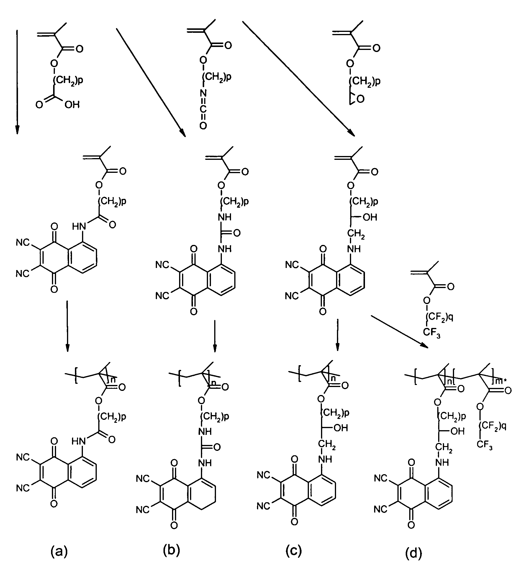
- side-chain polymers of formula I it is possible to polymerize monomers and/or oligomers which already carry the group Sp-G and/or the group R, for example by a chain-growth reaction, like free-radical or ionic polymerization, or a step-growth reaction, like polycondensation or polyaddition, including ring-opening polymerization and methathesis polymerization.
- a chain-growth reaction like free-radical or ionic polymerization
- a step-growth reaction like polycondensation or polyaddition, including ring-opening polymerization and methathesis polymerization.
- the invention further relates to a monomer of formula I1 P 11 -Sp-G wherein Sp and G are as defined in formula I, and P 11 is a polymerizable group which can react into a polymer backbone as formed by group P 1 .
- the invention further relates to a polymerizable material comprising one or more monomers of formula I1 and optionally comprising one or more monomers selected of formula I2 and/or I3 P 22 -R P 33 wherein R is as defined in formula I, P 22 is a polymerizable group which can react into a polymer backbone as formed by group P 2 , and P 33 is a monomer which upon polymerisation gives a polymer backbone as formed by group P 3 .
- the invention further relates to a polymer obtained by polymerization of a monomer of formula I1 or of a polymerizable material comprising one or more monomers of formula I1 and optionally comprising one or more momomers of formula I2.
- the group P 3 can also denote the unreacted form of group P 1 or P 2 resulting from an incomplete grafting reaction.
- group P 1 or P 2 resulting from an incomplete grafting reaction.
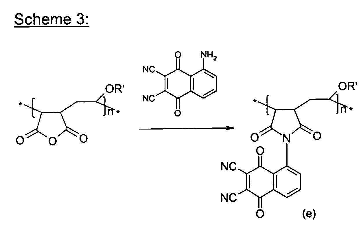
- a polymer (1b) as shown below is prepared by grafting a group G to a maleic anhydride polymer backbone (1a), some of the maleic anhydride units may remain unreacted, so that a copolymer comprising a mixture of substituted maleimide units (corresponding to P 1 ) and unsubstituted maleic anhydride units (corresponding to P 3 ) is obtained.
- R' is alkyl or alkoxy with 1 to 20 C atoms.
- the polymerizable groups P 11 and P 22 can be identical or different. Especially preferred are mixtures and copolymers wherein the polymerizable groups P 11 and P 22 are identical.
- P 33 is preferably a monomer capable of reacting into a polymer backbone as formed by group P 3 , or capable of reacting into a copolymer with P 11 and/or P 22 , thus extending the polymer chain.
- suitable and preferred monomers P 33 include vinyl ethers, styrenes, alkyl acrylates and alkylmethacrylates, vinylpyrrolidones, vinyl acetates and maleic acid derivatives.
- Further preferred are monomers P 33 selected of formula P 33 '-R", wherein P 33 ' has one of the preferred meanings of P 11 and P 22 as given above and R" is H or alkyl with 1 to 20 C atoms.
- the number of recurring units or the group p is preferably at least 5, very preferably at least 10, however, oligomers containing 3 to 15 monomer units are also possible.
- polymers in particular those of formula I, wherein the number of recurring units or p is from 10 to 500,000.
- polymers of formula I wherein in at least one recurring unit n is 1 and R is as defined above and below, preferably selected from C 1 -C 20 -fuoroalkyl, C 1 -C 15 -perfluoroalkyl, -(Si(R 0 R 00 )-O) r -R 000 and (CH 2 CH 2 O) s , wherein R 0 , R 00 and R 000 are independently of each other H or alkyl with 1 to 12 C-atoms, r is an integer from 1 to 15 and s is an integer from 1 to 6.
- Preferred spacer groups are selected of formula II X 1 -Sp 1 -X 2 wherein
- Typical groups Sp 1 are, for example, -(CH 2 ) t -, -(CH 2 CH 2 O) u -CH 2 CH 2 -, -CH 2 CH 2 -S-CH 2 CH 2 - or -CH 2 CH 2 -NH-CH 2 CH 2 - or -(SiR 0 R 00 -O) t -, with t being an integer from 2 to 12, u being an integer from 1 to 3 and R 0 and R 00 having the meanings given above.
- Preferred groups Sp 1 are for example ethylene, propylene, butylene, pentylene, hexylene, heptylene, octylene, nonylene, decylene, undecylene, dodecylene, octadecylene, ethyleneoxyethylene, methyleneoxybutylene, ethylene-thioethylene, ethylene-N-methyl-iminoethylene, 1-methylalkylene, ethenylene, propenylene and butenylene.
- X 1 and X 2 are preferably selected from -O-, -S-, -NR 0 -, -CO-, -COO-, -OCO-, -O-COO-, -CO-NR 0 -, -NR 0 -CO-, and a single bond, in particular from -CO-, -NR 0 -CO-, -CO-NR 0 - and a single bond.
- Especially preferred spacer groups are selected from the following formulae *-Alkyl-CO-NH- *-Alkyl-COO- *-Alkyl-O- *-Alkyl-NH- *-Alkyl- *-Alkyl-CH(OH)-CH 2 -NH- *-Alkyl-CH(OH)-CH 2 -O- wherein Alkyl denotes an alkyl, fluoroalkyl or oxaalkyl group with 1 to 15 C atoms, and the asterisk denotes the side that is linked to the polymer backbone.
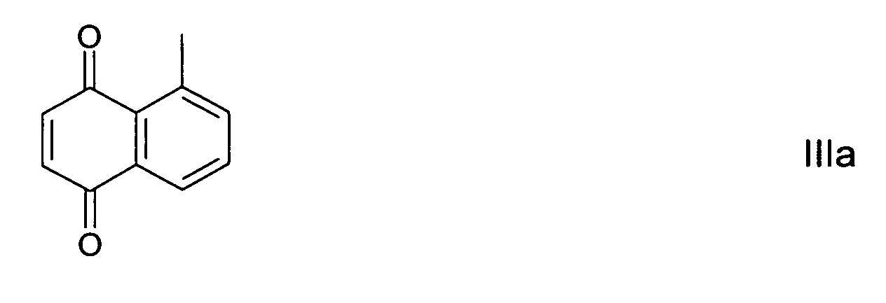
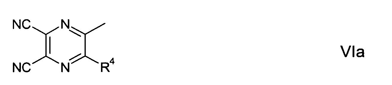
- Suitable and preferred electron accepting groups or groups G are selected from optionally substituted quinone or cyanoquinone, and aromatic or conjugated non aromatic groups that are mono- or polysubstituted by cyano, halo, haloalkyl, nitro or ester groups.
- the electron accepting group is selected of formula III wherein
- Especially preferred electron accepting groups are selected from the following formulae wherein R 4 has one of the meanings of R 3 given in formula III.
- the group R in formula I is an organic moiety that is designed to impart a lower surface energy to the polymer dopant, or reduce the actual surface energy of the polymer to below that of the semiconductor, and thus preferentially partition at the air interface of a polymer dopant - semiconductor blend.
- the group R should act as surfactant and is preferably selected from surface active groups.
- R is selected from C 1 -C 20 -fluoroalkyl, in particular C 1 -C 15 -perfluoroalkyl, -(Si(R 0 R 00 )-O) r -R, and (CH 2 CH 2 O) s , wherein R 0 , R 00 and R 000 are independently of each other H or alkyl with 1 to 12 C-atoms, r is an integer from 1 to 15 and s is an integer from 1 to 6.
- R and R 1-4 is an alkyl or alkoxy radical, i.e., where the terminal CH 2 group is replaced by -O-, this may be straight-chain or branched. It is preferably straight-chain, has 2 to 8 carbon atoms and accordingly is preferably ethyl, propyl, butyl, pentyl, hexyl, heptyl, octyl, ethoxy, propoxy, butoxy, pentoxy, hexyloxy, heptoxy, or octoxy, furthermore methyl, nonyl, decyl, undecyl, dodecyl, tridecyl, tetradecyl, pentadecyl, nonoxy, decoxy, undecoxy, dodecoxy, tridecoxy or tetradecoxy, for example.
- Fluoroalkyl or fluorinated alkyl or alkoxy is preferably straight chain (O)C i F 2i+1 , wherein i is an integer from 1 to 20, in particular from 1 to 15, very preferably (O)CF 3 , (O)C 2 F 5 , (O)C 3 F 7 , (O)C 4 F 9 , (O)C 5 F 11 , (O)C 6 F 13 , (O)C 7 F 15 or (O)C 8 F 17 .
- Halogen is preferably F, Br or Cl.
- the polymer dopants can be prepared by methods like polymerization reactions or polymer-analoguous reactions which are known per se and are described in the literature (for example in the standard works such as Odian, Principles of Polymerization, McGraw-Hill, New York), to be precise under reaction conditions which are known and suitable for the reactions. Use may also be made here of variants which are known per se, but are not described here in greater detail. Some preferred methods of preparing the polymer dopants are described below.
- polymerization is carried out as in-situ polymerization of a coated layer of a monomer of formula I1, or of a mixture comprising two or more monomers of formula I1 and optionally formula I2, for example in bulk or dissolved in a suitable solvent, preferably during fabrication of the electronic or optical device comprising the inventive semiconductor material.
- Polymerization can be initiated by exposing the monomers to heat or actinic radiation.
- Actinic radiation means irradiation with light, like UV light, IR light or visible light, irradiation with X-rays or gamma rays or irradiation with high energy particles, such as ions or electrons.
- Preferably polymerization is carried out by UV irradiation at a non-absorbing wavelength.
- a source for actinic radiation for example a single UV lamp or a set of UV lamps can be used. When using a high lamp power the curing time can be reduced.
- Another possible source for actinic radiation is a laser, like e.g. a UV laser, an IR laser or a visible laser.
- Polymerization is preferably carried out in the presence of an initiator absorbing at the wavelength of the actinic radiation.
- an initiator absorbing at the wavelength of the actinic radiation.
- a photoinitiator can be used that decomposes under UV irradiation to produce free radicals or ions that start the polymerization reaction.
- a radical photoinitiator is used
- curing polymerizable materials with vinyl, epoxide and oxetane groups preferably a cationic photoinitiator is used. It is also possible to use a polymerization initiator that decomposes when heated to produce free radicals or ions that start the polymerization.
- a photoinitiator for radical polymerization for example the commercially available Irgacure 651, Irgacure 184, Darocure 1173 or Darocure 4205 (all from Ciba Geigy AG) can be used, whereas in case of cationic photopolymerization the commercially available UVI 6974 (Union Carbide) can be used.
- the polymerizable material can additionally comprise one or more other suitable components such as, for example, catalysts, sensitizers, stabilizers, inhibitors, chain-transfer agents, co-reacting monomers, surface-active compounds, lubricating agents, wetting agents, dispersing agents, hydrophobing agents, adhesive agents, flow improvers, defoaming agents, deaerators, diluents, reactive diluents, auxiliaries, colourants, dyes or pigments.
- suitable components such as, for example, catalysts, sensitizers, stabilizers, inhibitors, chain-transfer agents, co-reacting monomers, surface-active compounds, lubricating agents, wetting agents, dispersing agents, hydrophobing agents, adhesive agents, flow improvers, defoaming agents, deaerators, diluents, reactive diluents, auxiliaries, colourants, dyes or pigments.
- Creating a thin layer of a polymer dopant on a semiconductor surface can be achieved in different ways.
- the polymer dopant or a solution of the polymer dopant, is dispensed directly on the semiconductor layer, and the solvent, if present, is evaporated to form a thin layer.
- an organic multilayer comprising at least one layer of an organic semiconductor material, and further comprising at least one layer of a polymer dopant according to the invention as described above, preferably selected of formula I or its preferred subformulae, which is in direct contact with said semiconductor layer.
- a multilayer is another object of the present invention.
- a formulation containing one or more semiconducting polymers and one or more dopant polymers is prepared, preferably dissolved in a suitable solvent, in which the dopant polymer is designed to exhibit a lower surface energy than the semiconducting polymer.
- the dopant polymer On dispensing this formulation to form a film, the dopant polymer, behaving like a surfactant, is driven by thermodynamics to the surface.
- the dopant polymer should preferably contain a doping component and a low energy component, like for example a fluorinated or siloxane functionality.
- a doping component and a low energy component like for example a fluorinated or siloxane functionality.
- An example for such a polymer is a copolymer of formula I wherein n is > 0, and wherein G represents the doping component and R the low energy component.
- an organic material with improved charge carrier mobility comprising one or more organic semiconducting components and one or more polymer dopant components, wherein at least one polymer dopant component is a polymer according to the present invention as described above and below, preferably a copolymer contain a doping component and a low energy component, very preferably selected of formula I or its preferred subformulae.
- Such an organic material is another object of the present invention.
- an organic material wherein the semiconductor and polymer dopant components form a mixture, solution, dispersion or polymer blend, optionally with further components.
- Another object of the invention is a monolithic film or layer of an organic material with improved charge carrier mobility, comprising one or more organic semiconducting components and one or more polymer dopant components as described above, wherein the polymer dopant components are predominantly situated at the surfaces of the film or layer.
- Another object of the invention is a semiconductor, electrical conductor, photoconductor, electrooptical or electronic material, component or device, comprising such an organic material or film.
- Films can be formed from solution by well known techniques such as spin coating, dip coating, spray coating, doctor blading as well as printing techniques including all types of gravure coating, ink jetting, stamping and screen printing.
- All common organic semiconducting materials are suitable candidates as the semiconducting host, including, but not limited to, polyalkylthiophenes, polythiophenes, polyfluorenes, polyphenylamines, and their copolymers, as well as small molecules such as pentacene, other polyacenes, and other fused ring compounds.
- a semiconducting and a polymer dopant material according to the present invention can be used as an organic "metal" in applications, for example, but not limited to, charge injection layers and ITO planarising layers in organic light emitting diode applications, films for flat panel displays and touch screens, antistatic films, printed conductive substrates, patterns or tracts in electronic applications such as printed circuit boards and condensers.
- the polymer dopants of the present invention are useful as dopants for optical, electronic and semiconductor materials, in particular for charge transport materials in field effect transistors (FETs), for photovoltaics or sensor materials, for electrophotographic recording materials, and for other semiconductor applications.
- FETs field effect transistors
- Such FETs where an organic semiconductive material is arranged as a film between a gate-dielectric and a drain and a source electrode, are generally known, e.g., from US 5,892,244, WO 00/79617, US 5,998,804, and from the references cited in the background and prior art chapter and listed below. Due to the advantages, like low cost production using the solubility properties of the compounds according to the invention and thus the processibility of large surfaces, preferred applications of these FETs are such as integrated circuitry, TFT-displays and security applications.
- field effect transistors and other devices with semiconductive materials may be used for ID tags or security markings to authenticate and prevent counterfeiting of documents of value like banknotes, credit cards or ID cards, national ID documents, licenses or any product with money value, like stamps, tickets, shares, cheques etc..
- the polymers according to the invention may be used as dopants in organic light emitting devices or diodes (OLEDs), e.g., in display applications or as backlight of e.g. liquid crystal displays.
- OLEDs organic light emitting devices or diodes
- Common OLEDs are realized using multilayer structures.
- An emission layer is generally sandwiched between one or more electron-transport and/ or hole-transport layers.
- By applying an electric voltage electrons and holes as charge carriers move towards the emission layer where their recombination leads to the excitation and hence luminescence of the lumophor units contained in the emission layer.
- the inventive materials may be employed in one or more of the charge transport layers and/ or in the emission layer, corresponding to their electrical and/ or optical properties.
Landscapes
- Chemical & Material Sciences (AREA)
- Engineering & Computer Science (AREA)
- Materials Engineering (AREA)
- Physics & Mathematics (AREA)
- Spectroscopy & Molecular Physics (AREA)
- Chemical Kinetics & Catalysis (AREA)
- Health & Medical Sciences (AREA)
- Medicinal Chemistry (AREA)
- Polymers & Plastics (AREA)
- Organic Chemistry (AREA)
- Manufacturing & Machinery (AREA)
- Electroluminescent Light Sources (AREA)
- Polyoxymethylene Polymers And Polymers With Carbon-To-Carbon Bonds (AREA)
- Addition Polymer Or Copolymer, Post-Treatments, Or Chemical Modifications (AREA)
- Processes Of Treating Macromolecular Substances (AREA)
Abstract
Description


- P1-3
- independently of each other denote a group forming a polymer backbone,
- Sp
- is a spacer group or a single bond,
- G
- is an electron accepting group,
- R
- is an organic group imparting a low surface energy to the polymer,
- m, n, o
- are independently of each other 0 or 1, wherein in each recurring unit ([P1(Sp-G)]m-[P2(R)]n [P3]o)p m + n + o > 0, and in at least one of these recurring units m is 1,
- p
- is an integer from 1 to 500,000.
- the electron accepting group is selected from optionally substituted quinone or cyanoquinone, or an aromatic or conjugated non aromatic group that is mono- or polysubstituted by cyano, halo, haloalkyl, nitro or ester groups, and/or
- the polymer comprises at least one organic group imparting a low surface energy to the polymer which is covalently bound, optionally via a spacer group, to the polymer backbone.
- the electron accepting group G is selected from optionally substituted quinone or cyanoquinone, or an aromatic or conjugated non aromatic group that is mono- or polysubstituted by cyano, halo, haloalkyl, nitro or ester groups, and/or
- in at least one recurring unit n is 1 and/or in at least one recurring unit o is 1.
- statistically random copolymers, for example with a monomer sequence such as -P1-P2-P1-P1-P3-P2-P1-P3-,
- alternating copolymers, for example with a monomer sequence such as -P1-P2-P1-P2- or P1-P2-P3-P1-P2-P3-, or
- block copolymers, for example with a monomer sequence such as -P1-P1-P1-P2-P2-P2-P3-P3-P3-,



- Sp1
- is alkylene with 1 to 20 C atoms which may be unsubstituted, mono- or poly-substituted by F, Cl, Br, I, CN or OH, it being also possible for one or more non-adjacent CH2 groups to be replaced, in each case independently from one another, by -O-, -S-, -NH-, -NR0-, -SiR0R00-, -CO-, -COO-, -OCO-, -OCO-O-, -S-CO-, -CO-S-, -CH=CH- or -C≡C- in such a manner that O and/or S atoms are not linked directly to one another, or a single bond,
- X1 and X2
- are independently of each other -O-, -S-, -NR0-, -CO-, -COO-, -OCO-, -O-COO-, -CO-NR0-, -NR0-CO-, -OCH2-, -CH2O-, -SCH2-, -CH2S-, -CF2O-, -OCF2-, -CF2S-, -SCF2-, -CF2CH2-, -CH2CF2-, -CF2CF2-, -CH=N-, -N=CH-, -N=N-, -CH=CH-, -CR0=CR00-, -CY1=CY2-, -C≡C-, -CH=CH-COO-, -OCO-CH=CH- or a single bond,
- Y1 and Y2
- are independently of each other H, F, Cl or CN and
- R0 and R00
- are independently of each other H or alkyl with 1 to 12 C-atoms.
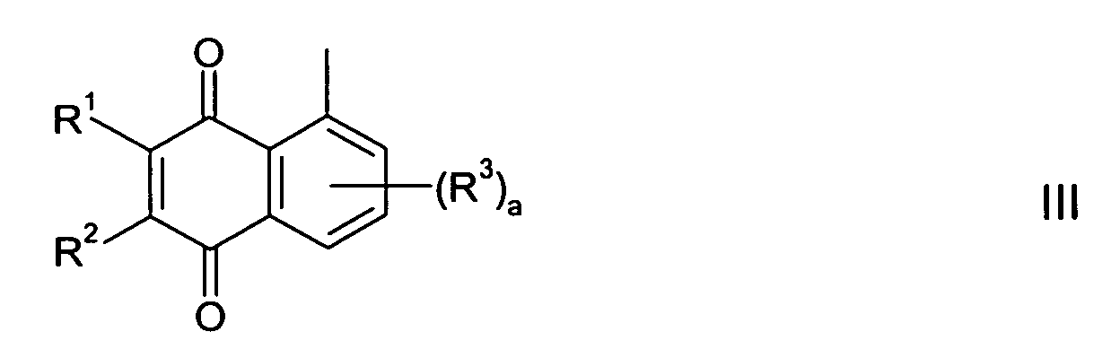
- R1 and R2
- are independently of each other H, halogen or CN,
- R3
- is in each occurrence independently of one another halogen, CN, NO2, NR0R00, or straight chain, branched or cyclic alkyl with 1 to 20 C-atoms, which is unsubstituted, mono- or polysubstituted by F, Cl, Br, I or CN, and wherein one or more non-adjacent CH2 groups are optionally replaced, in each case independently from one another, by -O-, -S-, -NH-, -NR0-, -SiR0R00-, -CO-, -COO-, -OCO-, -OCO-O-, -SO2-, -S-CO-, -CO-S-, -CH=CH- or -C≡C- in such a manner that O and/or S atoms are not linked directly to one another,
- R0 and R00
- are as defined in formula II, and
- a
- is 0, 1, 2 or 3.






Claims (26)
- Semiconductor or charge transport material, component or device, characterized in that it comprises a polymer comprising at least one electron accepting group as doping agent to induce or enhance charge carrier mobility or electrical conductivity.
- Semiconductor or charge transport material, component or device according to claim 1, characterized in that the electron accepting group is covalently incorporated in a polymer chain or covalently bound, optionally via a spacer group, to a polymer backbone.
- Semiconductor or charge transport material, component or device according to claim 1 or 2, characterized in that the doping polymer is selected of formula Iwherein

- P1-3
- independently of each other denote a group forming a polymer backbone,
- Sp
- is a spacer group or a single bond,
- G
- is an electron accepting group,
- R
- is an organic group that imparts a low surface energy to the polymer,
- m, n, o
- are independently of each other 0 or 1, wherein in each recurring unit ([P1(Sp-G)]m [P2(R)]n [P3]o)p m + n + o > 0, and in at least one of these recurring units m is 1,
- p
- is an integer from 1 to 500,000.
- Semiconductor or charge transport material, component or device according to claim 3, characterized in that p an integer from 10 to 500,000.
- Semiconductor or charge transport material, component or device according to claim 3, characterized in that R is selected from C1-C20-fuoroalkyl, C1-C15-perfluoroalkyl, -(Si(R0R00)-O)r-R and (CH2CH2O)s, wherein R0, R00 and R000 are independently of each other H or alkyl with 1 to 12 C-atoms, r is an integer from 1 to 15 and s is an integer from 1 to 6.
- Semiconductor or charge transport material, component or device according to at least one of claims 2 to 5, characterized in that the polymer backbone is selected from the group comprising maleic anhydride (co-)polymers, maleimide (co-) polymers, polyacrylpolyacrylate, polymethacrylate, poly-α-haloacrylate, poly-α-cyanoacrylate, polyacrylamide, polyacrylonitrile, polymethylene malonate, polymethylene maleimide, polyester, polyamide, polyimide, polyphosphazene, polyurethane, polysiloxane, polyepoxide, polyvinylalcohol, polyvinylether, polyvinlpyrrolidone, polyethyleneimine, polyalkylene, polycarbonate, polystyrene and copolymers thereof.
- Semiconductor or charge transport material, component or device according to at least one of claims 2 to 6, characterized in that the spacer group or group Sp is selected of formula II
- Sp1
- is alkylene with 1 to 20 C atoms which may be unsubstituted, mono- or poly-substituted by F, Cl, Br, I, CN or OH, it being also possible for one or more non-adjacent CH2 groups to be replaced, in each case independently from one another, by -O-, -S-, -NH-, -NR0-, -SiR0R00-, -CO-, -COO-, -OCO-, -OCO-O-, -S-CO-, -CO-S-, -CH=CH- or -C≡C- in such a manner that O and/or S atoms are not linked directly to one another, or a single bond,
- X1 and X2
- are independently of each other -O-, -S-, -NR0-, -CO-, -COO-, -OCO-, -O-COO-, -CO-NR0-, -NR0-CO-, -OCH2-, -CH2O-, -SCH2-, -CH2S-, -CF2O-, -OCF2-, -CF2S-, -SCF2-, -CF2CH2-, -CH2CF2-, -CF2CF2-, -CH=N-, -N=CH-, -N=N-, -CH=CH-, -CR0=CR00-, -CY1=CY2-, -C≡C-, -CH=CH-COO-, -OCO-CH=CH- or a single bond,
- Y1 and Y2
- are independently of each other H, F, Cl or CN and
- R0 and R00
- are independently of each other H or alkyl with 1 to 12 C-atoms.
- Semiconductor or charge transport material, component or device according to claim 7, characterized in that the spacer group or group Sp is selected from the following formulae,
- Semiconductor or charge transport material, component or device according to at least one of claims 1 to 8, characterized in that the electron accepting group or group G is selected of formula IIIwherein

- R1 and R2
- are independently of each other H, halogen or CN,
- R3
- is in each occurrence independently of one another H, halogen, CN, NO2, NR0R00, or straight chain, branched or cyclic alkyl with 1 to 20 C-atoms, which is unsubstituted, mono- or polysubstituted by F, Cl, Br, I or CN, and wherein one or more non-adjacent CH2 groups are optionally replaced, in each case independently from one another, by -O-, -S-, -NH-, -NR0-, -SiR0R00-, -CO-, -COO-, -OCO-, -OCO-O-, -SO2-, -S-CO-, -CO-S-, -CH=CH- or -C≡C- in such a manner that O and/or S atoms are not linked directly to one another,
- R0 and R00
- are as defined in formula II, and
- a
- is 0, 1, 2 or 3.
- Semiconductor or charge transport material, component or device according to at least one of claims 1 to 9, characterized in that the electron accepting group or group G is selected from optionally substituted quinone or cyanoquinone, or an aromatic or conjugated non aromatic group that is mono- or polysubstituted by cyano, halo, haloalkyl, nitro or ester groups.
- Semiconductor or charge transport material, component or device according to claim 10, characterized in that the electron accepting group or group G is selected from the following formulae

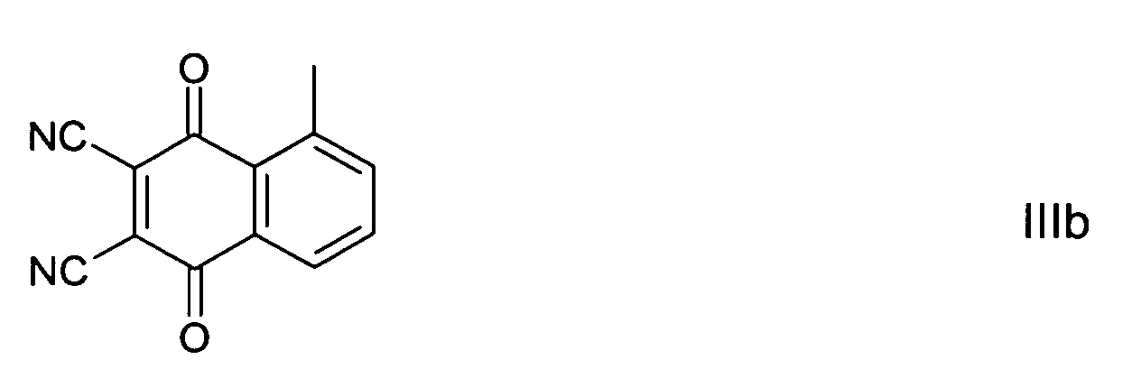
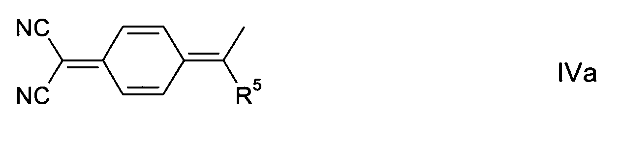



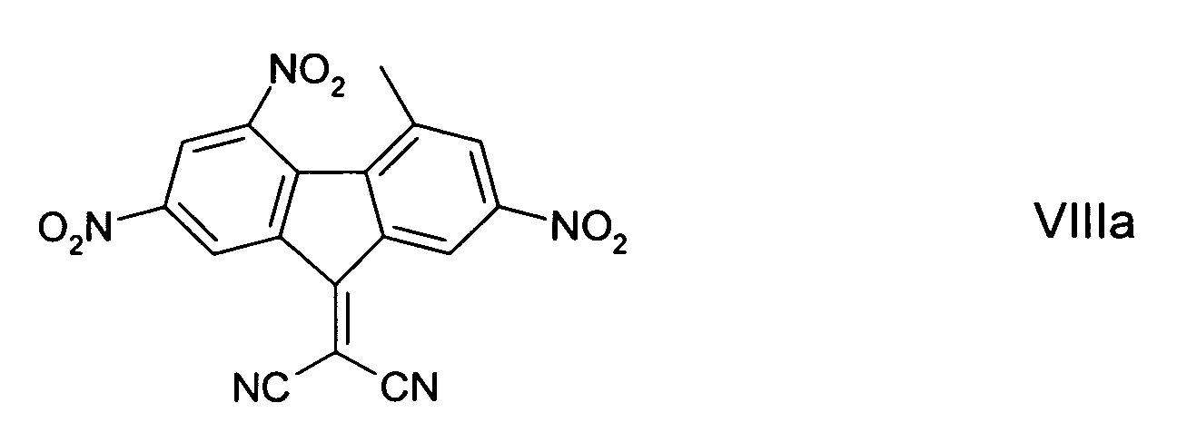 wherein R4 has one of the meanings of R3 given in formula III.
- Polymer as defined in at least one of claims 1 to 11, characterized in that it comprises an electron accepting group or group G as defined in claim 11 or 12.
- Polymer as defined in at least one of claims 1 to 12, characterized in that comprises at least one organic group imparting a low surface energy to the polymer which is covalently bound, optionally via a spacer group, to the polymer backbone.
- Polymer according to claim 12 or 13, characterized in that is selected of formula I as defined in at least one of claims 3 to 12.
- Monomer of formula I1
- Polymerizable material comprising one or more monomers according to claim 15 and optionally comprising one or more monomers selected of formula I2 and/or I3
- Polymer obtained by polymerization of a monomer according to claim 15 or a polymerizable material according to claim 16.
- Use of a polymer, monomer or polymerizable material as defined in at least one of claims 1 to 17 as doping agent in a semiconductor, electrical conductor or photoconductor component or material, in optical, electrooptical or electronic devices, field effect transistors (FET) as components of integrated circuitry, of thin film transistors (TFT) for flat panel display applications, or of radio frequency identification (RFID) tags, semiconducting components for organic light emitting diode (OLED) applications, including the charge transport and electroluminescent component in electroluminescent displays or backlights of flat panel displays or liquid crystal displays, in photovoltaic, photoconductor or sensor devices, as electrode material in batteries, and for electrophotographic applications like electrophotographic recording.
- Use according to claim 18, characterized in that the polymer forms a molecularly dissolved or dispersed polymer blend with a semiconducting polymer in a semiconductor matrix, or a discrete thin film layer that is in direct contact with a semiconductor material.
- Organic material with improved charge carrier mobility, characterized in that it comprises one or more organic semiconductor components and one or more polymer dopant components, wherein at least one polymer dopant component is a polymer as defined in at least one of claims 1 to 14 or 17.
- Organic material according to claim 20, characterized in that the semiconductor component(s) and the polymer dopant component(s) form a mixture, solution, dispersion or polymer blend, optionally with further components.
- Semiconductor, electrical conductor, photoconductor, electrooptical or electronic material, component or device, characterized in that it comprises an organic material according to claim 20 or 21.
- Semiconductor, electrical conductor, photoconductor, electrooptical or electronic material, component or device, comprising at least one layer of an organic semiconductor material, characterized in that it further comprises at least one layer of a polymer dopant as defined in at least one of claims 1 to 14 or 17 that is in direct contact with said semiconductor layer.
- Device according to claim 22 or 23, characterized in that it is a field effect transistor (FET), a charge transport or electroluminescent component in an organic light emitting diode (OLED), a photovoltaic, photoconductor or a sensor device, a battery electrode or part thereof, an electrophotographic or electrophotographic recording device, a charge injection layer, a Schottky diode, a planarising layer, an antistatic film or a conducting substrate or pattern.
- Integrated circuit (IC), thin film transistor (TFT), radio frequency identification (RFID) tag, organic light emitting diode (OLED), electroluminescent display, backlight, flat panel display, liquid crystal display, battery or sensor, characterized in that it comprises a material, component or device according to at least one of claims 22 to 24.
- Security marking or device, characterized in that it comprises a FET or an RFID tag according to claim 24 or 25.
Priority Applications (1)
| Application Number | Priority Date | Filing Date | Title |
|---|---|---|---|
| EP04000196A EP1441399A3 (en) | 2003-01-25 | 2004-01-08 | Polymer dopants |
Applications Claiming Priority (3)
| Application Number | Priority Date | Filing Date | Title |
|---|---|---|---|
| EP03001678 | 2003-01-25 | ||
| EP03001678 | 2003-01-25 | ||
| EP04000196A EP1441399A3 (en) | 2003-01-25 | 2004-01-08 | Polymer dopants |
Publications (2)
| Publication Number | Publication Date |
|---|---|
| EP1441399A2 true EP1441399A2 (en) | 2004-07-28 |
| EP1441399A3 EP1441399A3 (en) | 2009-07-01 |
Family
ID=32598809
Family Applications (1)
| Application Number | Title | Priority Date | Filing Date |
|---|---|---|---|
| EP04000196A Withdrawn EP1441399A3 (en) | 2003-01-25 | 2004-01-08 | Polymer dopants |
Country Status (1)
| Country | Link |
|---|---|
| EP (1) | EP1441399A3 (en) |
Cited By (4)
| Publication number | Priority date | Publication date | Assignee | Title |
|---|---|---|---|---|
| WO2008127068A1 (en) | 2007-04-16 | 2008-10-23 | Lg Chem, Ltd. | Optical film and liquid crystal display comprising the same |
| US8314416B2 (en) | 2006-03-24 | 2012-11-20 | Merck Patent Gmbh | Organic semiconductor formulation |
| US8741442B2 (en) | 2005-04-15 | 2014-06-03 | General Electric Company | Modified electrodes using functional organic materials and electronic devices therefrom |
| WO2017089811A1 (en) * | 2015-11-25 | 2017-06-01 | Cambridge Display Technology Limited | Charge transfer salt, electronic device and method of forming the same |
Family Cites Families (3)
| Publication number | Priority date | Publication date | Assignee | Title |
|---|---|---|---|---|
| US5185102A (en) * | 1989-06-08 | 1993-02-09 | Minnesota Mining And Manufacturing Company | Polymeric charge transfer complexes for nonlinear optical applications |
| JPH0836200A (en) * | 1994-07-25 | 1996-02-06 | Mitsubishi Chem Corp | Polymer materials for nonlinear optics |
| ATE410791T1 (en) * | 1999-04-06 | 2008-10-15 | Cambridge Display Tech Ltd | METHOD FOR DOPPING POLYMERS |
-
2004
- 2004-01-08 EP EP04000196A patent/EP1441399A3/en not_active Withdrawn
Cited By (5)
| Publication number | Priority date | Publication date | Assignee | Title |
|---|---|---|---|---|
| US8741442B2 (en) | 2005-04-15 | 2014-06-03 | General Electric Company | Modified electrodes using functional organic materials and electronic devices therefrom |
| US8314416B2 (en) | 2006-03-24 | 2012-11-20 | Merck Patent Gmbh | Organic semiconductor formulation |
| WO2008127068A1 (en) | 2007-04-16 | 2008-10-23 | Lg Chem, Ltd. | Optical film and liquid crystal display comprising the same |
| EP2137243A4 (en) * | 2007-04-16 | 2010-04-14 | Lg Chemical Ltd | OPTICAL FILM AND LIQUID CRYSTAL DISPLAY COMPRISING THE SAME |
| WO2017089811A1 (en) * | 2015-11-25 | 2017-06-01 | Cambridge Display Technology Limited | Charge transfer salt, electronic device and method of forming the same |
Also Published As
| Publication number | Publication date |
|---|---|
| EP1441399A3 (en) | 2009-07-01 |
Similar Documents
| Publication | Publication Date | Title |
|---|---|---|
| US7186358B2 (en) | Polymer dopants | |
| US7244809B2 (en) | Mono-, oligo- and polymers comprising dithienothiophene and aryl groups | |
| US7524922B2 (en) | Poly(benzodithiophenes) | |
| US7126013B2 (en) | Mono-, oligo- and polymers comprising fluorene and aryl groups | |
| JP4942910B2 (en) | Monomers, oligomers and poly (3-alkynylthiophenes) and their use as charge transfer materials | |
| US6695978B2 (en) | Mono-, oligo- and polymers of benzo[b]thiophene and 2,2′-bisbenzo[b]thiophene and their use as charge transport materials | |
| US7470377B2 (en) | Monomers, oligomers and polymers comprising thiophene and selenophene | |
| US20040119049A1 (en) | Mono-, oligo- and poly-bis(thienyl) arylenes and their use as charge transport materials | |
| KR20030007053A (en) | Thienothiophene derivatives | |
| EP1891077A1 (en) | Monomers , oligomers and polymers of thieno (3, 4-d) thiazole | |
| EP1477504A1 (en) | Mono-, oligo- and polymers comprising dithienotiophene and aryl groups | |
| EP1300430B1 (en) | Mono-, oligo- and polymers of benzo(b)thiophene and 2,2'-bisbenzo(b)thiophene and their use as charge transport materials | |
| EP1357163A1 (en) | Reactive mesogenic benzodithiophenes | |
| EP1398336B1 (en) | Mono-, Oligo- and Poly(3-alkynylthiophenes) and their Use as Charge Transport Materials | |
| EP1439590A2 (en) | Mono-, oligo- and poly-bis(thienyl) arylenes and their use as charge transport materials | |
| EP1441399A2 (en) | Polymer dopants | |
| EP1284258A2 (en) | Mono-, oligo- and polyalkylidenefluorenes and their use as charge transport materials | |
| EP1279690A1 (en) | Mono-oligo- and poly-3-substituted-4-fluorothiophenes and their use as charge transport materials | |
| JP2009520044A (en) | Regioregular polyselenophenes | |
| EP1318185B1 (en) | Reactive mesogenic azulenes | |
| EP1475401B1 (en) | Mono-, oligo- and polymers comprising fluorene and aryl groups |
Legal Events
| Date | Code | Title | Description |
|---|---|---|---|
| PUAI | Public reference made under article 153(3) epc to a published international application that has entered the european phase |
Free format text: ORIGINAL CODE: 0009012 |
|
| 17P | Request for examination filed |
Effective date: 20040108 |
|
| AK | Designated contracting states |
Kind code of ref document: A2 Designated state(s): AT BE BG CH CY CZ DE DK EE ES FI FR GB GR HU IE IT LI LU MC NL PT RO SE SI SK TR |
|
| AX | Request for extension of the european patent |
Extension state: AL LT LV MK |
|
| PUAL | Search report despatched |
Free format text: ORIGINAL CODE: 0009013 |
|
| AK | Designated contracting states |
Kind code of ref document: A3 Designated state(s): AT BE BG CH CY CZ DE DK EE ES FI FR GB GR HU IE IT LI LU MC NL PT RO SE SI SK TR |
|
| AX | Request for extension of the european patent |
Extension state: AL LT LV MK |
|
| AKX | Designation fees paid |
Designated state(s): AT BE BG CH CY CZ DE DK EE ES FI FR GB GR HU IE IT LI LU MC NL PT RO SE SI SK TR |
|
| STAA | Information on the status of an ep patent application or granted ep patent |
Free format text: STATUS: THE APPLICATION IS DEEMED TO BE WITHDRAWN |
|
| 18D | Application deemed to be withdrawn |
Effective date: 20100105 |