EP1441363A2 - Ferroelectric resistor non-volatile memory array - Google Patents
Ferroelectric resistor non-volatile memory array Download PDFInfo
- Publication number
- EP1441363A2 EP1441363A2 EP04250175A EP04250175A EP1441363A2 EP 1441363 A2 EP1441363 A2 EP 1441363A2 EP 04250175 A EP04250175 A EP 04250175A EP 04250175 A EP04250175 A EP 04250175A EP 1441363 A2 EP1441363 A2 EP 1441363A2
- Authority
- EP
- European Patent Office
- Prior art keywords
- resistor
- array
- transistor
- voltage
- programming
- Prior art date
- Legal status (The legal status is an assumption and is not a legal conclusion. Google has not performed a legal analysis and makes no representation as to the accuracy of the status listed.)
- Withdrawn
Links
Images



Classifications
-
- G—PHYSICS
- G11—INFORMATION STORAGE
- G11C—STATIC STORES
- G11C11/00—Digital stores characterised by the use of particular electric or magnetic storage elements; Storage elements therefor
- G11C11/21—Digital stores characterised by the use of particular electric or magnetic storage elements; Storage elements therefor using electric elements
- G11C11/22—Digital stores characterised by the use of particular electric or magnetic storage elements; Storage elements therefor using electric elements using ferroelectric elements
- G11C11/225—Auxiliary circuits
- G11C11/2275—Writing or programming circuits or methods
-
- G—PHYSICS
- G11—INFORMATION STORAGE
- G11C—STATIC STORES
- G11C11/00—Digital stores characterised by the use of particular electric or magnetic storage elements; Storage elements therefor
- G11C11/21—Digital stores characterised by the use of particular electric or magnetic storage elements; Storage elements therefor using electric elements
- G11C11/22—Digital stores characterised by the use of particular electric or magnetic storage elements; Storage elements therefor using electric elements using ferroelectric elements
-
- G—PHYSICS
- G11—INFORMATION STORAGE
- G11C—STATIC STORES
- G11C11/00—Digital stores characterised by the use of particular electric or magnetic storage elements; Storage elements therefor
- G11C11/21—Digital stores characterised by the use of particular electric or magnetic storage elements; Storage elements therefor using electric elements
- G11C11/22—Digital stores characterised by the use of particular electric or magnetic storage elements; Storage elements therefor using electric elements using ferroelectric elements
- G11C11/225—Auxiliary circuits
- G11C11/2273—Reading or sensing circuits or methods
-
- G—PHYSICS
- G11—INFORMATION STORAGE
- G11C—STATIC STORES
- G11C5/00—Details of stores covered by group G11C11/00
- G11C5/06—Arrangements for interconnecting storage elements electrically, e.g. by wiring
- G11C5/063—Voltage and signal distribution in integrated semi-conductor memory access lines, e.g. word-line, bit-line, cross-over resistance, propagation delay
-
- G—PHYSICS
- G11—INFORMATION STORAGE
- G11C—STATIC STORES
- G11C7/00—Arrangements for writing information into, or reading information out from, a digital store
- G11C7/18—Bit line organisation; Bit line lay-out
-
- G—PHYSICS
- G11—INFORMATION STORAGE
- G11C—STATIC STORES
- G11C8/00—Arrangements for selecting an address in a digital store
- G11C8/14—Word line organisation; Word line lay-out
Definitions
- This invention relates to ferroelectric non-volatile memory arrays, and specifically to a memory array which features a non-destructive read and which functions similarly to a constant current memory device.
- ITIC memory cells and single transistor ferroelectric-based devices are used as memory storage devices.
- ITIC memory is non-volatile, it is read destructive, i.e., the stored data is lost during a read operation, requiring refreshment of the cell.
- a read operation in a single transistor memory is non-destructive, however, because there is a relatively large field across the ferroelectric capacitor during standby conditions, there is a significant reduction in memory retention time.
- a ferroelectric thin film resistor memory array is formed on a substrate and includes plural memory cells arranged in an array of rows and columns; wherein each memory cell includes: FE resistor having a pair of terminals, and a transistor associated with each resistor, wherein each transistor has a gate, a drain and a source, and wherein the drain of each transistor is electrically connected to one terminal of its associated resistor; a word line connected to the gate of each transistor in a row; a programming line connected to each memory cell in a column; and a bit line connected to each memory cell in a column.
- the programming line is connected to the FE resistor other terminal and the bit line is connected to the transistor source, while in another embodiment, the programming line is connected to the transistor source and the bit line is connected to the FE resistor other terminal. In the latter embodiment, the programming line is suitable for function as a block erase line.
- Another object of the invention is to provide a memory array which function similarly to a constant current array.
- a basic non-volatile non-destructive read memory ferroelectric memory cell suitable for RAM application is disclosed in the related patent and application.
- the invention hereof is a large scale RAM circuit incorporating the previously disclosed memory cell.
- the basic circuit structure is similar to that of an ITIC ferroelectric memory with a modified memory operation circuit.
- the basic cell configuration is shown in Fig. 1, generally at 10.
- the ferroelectric capacitor of the ITIC cell is replaced with a memory resistor 12, and the "drive line” is replaced with a "programming line” 14.
- a transistor 15 includes a gate, a source and a drain, while memory resistor 12 includes a pair of terminals, one of which is connected to the drain of transistor 15.
- a bit line 16 and a word line 18 are provided. In this embodiment of the array of the invention, word line 18 is connected to transistor 15 gate, bit line 16 is connected to the transistor 15 source, and programming line 14 is connected to the other terminal of memory resistor 12.
- the programming and memory reading pulses are depicted in Fig. 2.
- Fig. 2a depicts a low current state
- Fig. 2b depicts a high current state
- Fig. 2c depicts a reading state.
- the amplitude of the programming pulse is between about 2V to 5V, depending on the voltage required for ferroelectric thin film polarization.
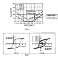
- the read pulse is a constant current pulse of between about 10nA to 100nA for the device having the I-V characteristics specifically shown in Figs. 3 and 4. Again the amplitude and the pulse width is dependent on the actual memory resistor property, principally the ferroelectric properties.
- the amplitude of the constant current is selected such that the voltage across the memory resistor is lower than the coercive voltage of the device.
- FIGs. 5a and 5b depict the hysteresis loops of PGO and PZT thin film resistors, respectively.
- the PGO hysteresis loop demonstrates a well defined coercive voltage of about IV, however, there is no well defined coercive voltage for the PZT hysteresis loop.
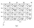
- Fig. 6 depicts a 16-bit equivalent circuit of the array of the invention, generally at 30, where W1 - W4 are word lines; B1- B4 are bit lines; and P1 - P4 are programming lines.
- T 11 - T 44 and FE 11 - FE 44 are the bit transistors and bit memory resistors, respectively.
- a memory resistor of this example is constructed and arranged to provide a constant current reading at a voltage of between about zero volts and 1+ volts, for example.
- a memory resistor of this example is constructed and arranged to provide a constant voltage reading at a voltage less than 0.5V. More preferably, a memory resistor of this example is constructed and arranged to provide a constant voltage reading at a voltage less than 0.2V.
- a memory resistor of this example is constructed and arranged to provide a programming voltage in a range of between about 2V and 5V, for example.
- a programming pulse, +V P is applied to W2, which turns on all transistors connected to W2.
- a programming pulse is applied to P2. Because the resistance of the memory resistor is very high, the voltage drop in transistor T 22 is very small. The voltage across memory resistor FE 22 is nearly equal to the amplitude of the programming pulse, V P . All other transistors connected to W2 line are turned on, however, because their programming lines and bit lines are at ground potential, they do not achieve a high current state. Because the gate of all transistors connected to B2, except T 22 , are at the ground potential, only memory resistor FE 22 is polarized, The memory contents of all other memory resistors are not changed. To block erase the memory array, a programming pulse, +V P , is applied to all P-lines and W-lines, while all B-lines are grounded. This programs all memory resistors to a high current state.
- the above process may be applied to program any memory bit in the array.
- All word lines, bit lines, and programming lines are grounded, except W3 and B3.
- An operation voltage, V CC is applied to W3 and a constant current of between about 10 ⁇ A to 100 ⁇ A is applied to B3.
- Bit line B3 is also connected to a sense amplifier to measure the voltage across the memory resistor.
- the voltage detected at the sense amplifier is the sum of the voltages across the memory resistor and that across the bit transistor. Because the voltage across the memory resistor is less than the coercive voltage of the ferroelectric thin film, the detected voltage is less than 1V.
- a bit line drive voltage source may be a simple MOST 56, preferably a pMOST, connected in series to the output of a bit line 58 of decoder 54.
- the gate voltage of T1 is biased to V P .
- the gate voltage of T1 is biased to deliver a given constant current of between about 10 ⁇ A to 100 ⁇ A.
- the low memory voltage is selected to be lower than the threshold voltage of the output inverter, while the high memory voltage state is higher than the turn-on voltage of the output inverter.
- the output of the memory is able to switch the sense inverter without an additional sense amplifier.
- the array may be block erased by applying the erase voltage to all programming lines and all word lines, while simultaneously grounding all bit lines.
- the array of the invention may be used for constant voltage operation, it is not a true constant voltage array.
- the bit line voltage is set to be lower than 0.5V to prevent read errors.
- the bit output is measured by connecting a current sensing amplifier at the programming line.
- the array of Fig. 6 provides high-speed programming when setting the memory resistor to its high-current state
- the programming line of Fig. 6 is biased with a positive voltage and the memory resistor is connected to the drain of the bit transistor, it has a relative slower speed when setting the memory resistor to it low current state, because, as +V P is applied to the bit line, the memory cell operates as a source follower, resulting in a slower programming speed to the low current state.
- This does not have a large impact on operating speed when the memory array is programmed one bit at a time, however, total programming time may be much greater for a block erase operation, wherein a block of memory is erased to the high current state, followed by programming of individual cells to the low current stale.
- the embodiment of the memory array depicted in Fig. 8, generally at 60 is suitable.
- the transistor drain is connected to memory resistor one terminal
- word lines are still connected to the gates of the transistor in each cell
- bit lines are connected to the FE resistor other terminal
- a programming line 62 also referred to herein as a block erase line, is connected to the source of the transistors in the array.
Landscapes
- Engineering & Computer Science (AREA)
- Computer Hardware Design (AREA)
- Microelectronics & Electronic Packaging (AREA)
- Semiconductor Memories (AREA)
- Non-Volatile Memory (AREA)
- Read Only Memory (AREA)
Abstract
Description
Claims (20)
- A ferroelectric thin film resistor memory array formed on a substrate comprising:. wherein, said memory cells are programmed using a programming voltage; andplural memory cells arranged in an array of rows and columns; wherein each memory cell includes:FE resistor having a pair of terminals, anda transistor associated with each resistor, wherein each transistor has a gate, a drain and a source, and wherein said drain of each transistor is electrically connected to one terminal of its associated resistor;a word line connected to the gate of each transistor in a row;a programming line connected to each memory cell in a column; anda bit line connected to each memory cell in a column;
wherein the ferroelectric resistor is non-destructively read by sensing taken from the group of sensing consisting of constant voltage sensing and constant current sensing. - The array of claim 1 wherein said FE resistor is constructed and arranged to provide a constant current reading at a voltage of between about zero volts and 1+ volts.
- The array of claim wherein said FE resistor is constructed and arranged to provide a constant voltage reading at a voltage less than 0.5V.
- The array of claim 3 wherein said FE resistor is constructed and arranged to provide a constant voltage reading at a voltage less than 0.2V.
- The array of claim 3 wherein said FE resistor is constructed and arranged to provide a programming voltage in a range of between about 2 V and 5 V.
- The array of claim 1 wherein said programming line is connected to said FB resistor other terminal and wherein said bit line is connected to said transistor source.
- The array of claim 1 wherein said programming line is connected to said transistor source and wherein said bit line is connected to said FE resistor other terminal.
- The array of claim 7 wherein said programming line is a block erase line.
- A ferroelectric thin film resistor memory array formed on a substrate comprising:wherein said FE resistor is constructed and arranged to provide a constant current reading at a voltage of between about zero volts and 1+ volts to provide a programming voltage in a range of between about 2 V and 5 V.plural memory cells arranged in an array of rows and columns; wherein each memory cell includes:FE resistor having a pair of terminals, anda transistor associated with each resistor, wherein each transistor has a gate, a drain and a source, and wherein said drain of each transistor is electrically connected to one terminal of its associated resistor;a word line connected to the gate of each transistor in a row;a programming line connected to each memory cell in a column; anda bit line connected to each memory cell in a column;
- The array of claim 9 wherein said programming line is connected to said FE resistor other terminal and wherein said bit line is connected to said transistor source.
- The array of claim 9 wherein said programming line is connected to said transistor source and wherein said bit line is connected to said FE resistor other terminal.
- The array of claim 11 wherein said programming line is a block erase line.
- The array of claim 9 wherein said FE resistor is constructed and arranged to provide a constant voltage reading at a voltage less than 0.5V.
- The array of claim 13 wherein said FE resistor is constructed and arranged to provide a constant voltage reading at a voltage less than 0.2V.
- A ferroelectric thin film resistor memory array formed on a substrate comprising:plural memory cells arranged in an array of rows and columns; wherein each memory cell includes:FE resistor having a pair of terminals, anda transistor associated with each resistor, wherein each transistor has a gate, a drain and a source, and wherein said drain of each transistor is electrically connected to one terminal of its associated resistor,a word line connected to the gate of each transistor in a row;a programming line connected to each memory cell in a column; anda bit line connected to each memory cell in a column.
- The array of claim 15 wherein said programming line is connected to said FE resistor other terminal and wherein said bit line is connected to said transistor source.
- The array of claim 15 wherein said programming line is connected to said transistor source and wherein said bit line is connected to said FE resistor other terminal.
- The array of claim 15 wherein said FE resistor is constructed and arranged to provide a constant current reading at a voltage of between about zero volts and 1+ volts.
- The array of claim 18 wherein said FE resistor is constructed and arranged to provide a programming voltage in a range of between about 2 V and 5 V.
- The array of claim 15 wherein, said memory cells are programmed using a programming voltage; and wherein the ferroelectric resistor is non-destructively read by sensing taken from the group of sensing consisting of constant voltage sensing and constant current sensing.
Applications Claiming Priority (2)
| Application Number | Priority Date | Filing Date | Title |
|---|---|---|---|
| US10/345,726 US6819583B2 (en) | 2003-01-15 | 2003-01-15 | Ferroelectric resistor non-volatile memory array |
| US345726 | 2003-01-15 |
Publications (2)
| Publication Number | Publication Date |
|---|---|
| EP1441363A2 true EP1441363A2 (en) | 2004-07-28 |
| EP1441363A3 EP1441363A3 (en) | 2004-10-06 |
Family
ID=32594868
Family Applications (1)
| Application Number | Title | Priority Date | Filing Date |
|---|---|---|---|
| EP04250175A Withdrawn EP1441363A3 (en) | 2003-01-15 | 2004-01-15 | Ferroelectric resistor non-volatile memory array |
Country Status (5)
| Country | Link |
|---|---|
| US (1) | US6819583B2 (en) |
| EP (1) | EP1441363A3 (en) |
| JP (1) | JP4187664B2 (en) |
| KR (1) | KR100536505B1 (en) |
| TW (1) | TWI243380B (en) |
Families Citing this family (11)
| Publication number | Priority date | Publication date | Assignee | Title |
|---|---|---|---|---|
| US7180141B2 (en) * | 2004-12-03 | 2007-02-20 | Texas Instruments Incorporated | Ferroelectric capacitor with parallel resistance for ferroelectric memory |
| US7515457B2 (en) * | 2006-02-24 | 2009-04-07 | Grandis, Inc. | Current driven memory cells having enhanced current and enhanced current symmetry |
| JP4460552B2 (en) * | 2006-07-04 | 2010-05-12 | シャープ株式会社 | Semiconductor memory device |
| US7764537B2 (en) * | 2007-04-05 | 2010-07-27 | Qualcomm Incorporated | Spin transfer torque magnetoresistive random access memory and design methods |
| US9129845B2 (en) | 2007-09-19 | 2015-09-08 | Micron Technology, Inc. | Buried low-resistance metal word lines for cross-point variable-resistance material memories |
| IT1400933B1 (en) | 2010-06-21 | 2013-07-02 | St Microelectronics Srl | TOUCH SENSOR AND METHOD OF FORMING A TOUCH SENSOR. |
| US8488361B2 (en) | 2011-02-01 | 2013-07-16 | Stmicroelectronics S.R.L. | Memory support provided with memory elements of ferroelectric material and improved non-destructive reading method thereof |
| ITTO20110181A1 (en) | 2011-02-01 | 2012-08-02 | St Microelectronics Srl | MEMORIZATION SUPPORT PROVIDED WITH ELEMENTS OF RAILWAY MATERIAL AND ITS NON-DESTRUCTIVE READING METHOD |
| EP2608210B1 (en) | 2011-12-23 | 2019-04-17 | IMEC vzw | Stacked RRAM array with integrated transistor selector |
| US11114149B2 (en) * | 2019-11-13 | 2021-09-07 | Wuxi Petabyte Technologies Co, Ltd. | Operation methods of ferroelectric memory |
| US12183397B2 (en) * | 2021-05-13 | 2024-12-31 | Taiwan Semiconductor Manufacturing Company, Ltd. | Memory circuits and devices, and methods thereof |
Family Cites Families (5)
| Publication number | Priority date | Publication date | Assignee | Title |
|---|---|---|---|---|
| US3775843A (en) * | 1970-08-07 | 1973-12-04 | R Wendt | Method of making temperature responsive apparatus |
| US5070385A (en) * | 1989-10-20 | 1991-12-03 | Radiant Technologies | Ferroelectric non-volatile variable resistive element |
| US5926412A (en) * | 1992-02-09 | 1999-07-20 | Raytheon Company | Ferroelectric memory structure |
| DE19832995C1 (en) * | 1998-07-22 | 1999-11-04 | Siemens Ag | Memory device using resistive ferroelectric memory cells |
| JP2002368109A (en) * | 2001-06-07 | 2002-12-20 | Umc Japan | Semiconductor device and manufacturing method thereof |
-
2003
- 2003-01-15 US US10/345,726 patent/US6819583B2/en not_active Expired - Fee Related
-
2004
- 2004-01-15 JP JP2004007472A patent/JP4187664B2/en not_active Expired - Fee Related
- 2004-01-15 EP EP04250175A patent/EP1441363A3/en not_active Withdrawn
- 2004-01-15 KR KR10-2004-0002875A patent/KR100536505B1/en not_active Expired - Fee Related
- 2004-01-15 TW TW093101025A patent/TWI243380B/en not_active IP Right Cessation
Also Published As
| Publication number | Publication date |
|---|---|
| US20040136223A1 (en) | 2004-07-15 |
| EP1441363A3 (en) | 2004-10-06 |
| TWI243380B (en) | 2005-11-11 |
| JP2004220764A (en) | 2004-08-05 |
| JP4187664B2 (en) | 2008-11-26 |
| KR20040066034A (en) | 2004-07-23 |
| KR100536505B1 (en) | 2005-12-14 |
| TW200425139A (en) | 2004-11-16 |
| US6819583B2 (en) | 2004-11-16 |
Similar Documents
| Publication | Publication Date | Title |
|---|---|---|
| KR100558209B1 (en) | Ferroelectric memory and how it works | |
| JP3913906B2 (en) | Ferroelectric random access memory device | |
| US6449184B2 (en) | Method for driving semiconductor memory | |
| US12283346B2 (en) | Locally embedded bad sector marking for a memory | |
| US8274842B1 (en) | Variable impedance memory device having simultaneous program and erase, and corresponding methods and circuits | |
| US6970370B2 (en) | Ferroelectric write once read only memory for archival storage | |
| US20160343422A1 (en) | Virtual ground sensing circuitry and related devices, systems, and methods | |
| US9361976B2 (en) | Sense amplifier including a single-transistor amplifier and level shifter and methods therefor | |
| US6754094B2 (en) | Circuit and method for testing a ferroelectric memory device | |
| US9805793B2 (en) | Filament confinement in reversible resistance-switching memory elements | |
| US9224466B1 (en) | Dual capacitor sense amplifier and methods therefor | |
| US6614678B2 (en) | Semiconductor memory and method for driving the same | |
| US7154768B2 (en) | Non-destructive readout of ferroelectric memories | |
| EP1441363A2 (en) | Ferroelectric resistor non-volatile memory array | |
| US20180277208A1 (en) | Methods and apparatus for programming barrier modulated memory cells | |
| DE102021115236A1 (en) | SIGNAL PRESERVATION IN MRAM WHILE READING | |
| KR101783933B1 (en) | Memory cell and memory device using the same | |
| JP2002150783A (en) | Semiconductor memory device and method of determining change in threshold value of memory cell transistor | |
| US6809954B1 (en) | Circuit and method for reducing access transistor gate oxide stress | |
| US6906945B2 (en) | Bitline precharge timing scheme to improve signal margin | |
| US6760246B1 (en) | Method of writing ferroelectric field effect transistor | |
| US6584009B1 (en) | Memory integrated circuit with improved reliability | |
| US7349237B2 (en) | Plateline driver with RAMP rate control | |
| US7177174B2 (en) | Ferroelectric memory device having a reference voltage generating circuit | |
| US6385077B1 (en) | Non-volatile memory cell and sensing method |
Legal Events
| Date | Code | Title | Description |
|---|---|---|---|
| PUAI | Public reference made under article 153(3) epc to a published international application that has entered the european phase |
Free format text: ORIGINAL CODE: 0009012 |
|
| AK | Designated contracting states |
Kind code of ref document: A2 Designated state(s): AT BE BG CH CY CZ DE DK EE ES FI FR GB GR HU IE IT LI LU MC NL PT RO SE SI SK TR |
|
| AX | Request for extension of the european patent |
Extension state: AL LT LV MK |
|
| PUAL | Search report despatched |
Free format text: ORIGINAL CODE: 0009013 |
|
| AK | Designated contracting states |
Kind code of ref document: A3 Designated state(s): AT BE BG CH CY CZ DE DK EE ES FI FR GB GR HU IE IT LI LU MC NL PT RO SE SI SK TR |
|
| AX | Request for extension of the european patent |
Extension state: AL LT LV MK |
|
| 17P | Request for examination filed |
Effective date: 20050406 |
|
| AKX | Designation fees paid |
Designated state(s): DE FR GB |
|
| 17Q | First examination report despatched |
Effective date: 20061214 |
|
| STAA | Information on the status of an ep patent application or granted ep patent |
Free format text: STATUS: THE APPLICATION IS DEEMED TO BE WITHDRAWN |
|
| 18D | Application deemed to be withdrawn |
Effective date: 20090220 |