EP1439583A1 - Sublithographic contact structure, in particular for a phase change memory cell, and fabrication process thereof - Google Patents
Sublithographic contact structure, in particular for a phase change memory cell, and fabrication process thereof Download PDFInfo
- Publication number
- EP1439583A1 EP1439583A1 EP03425016A EP03425016A EP1439583A1 EP 1439583 A1 EP1439583 A1 EP 1439583A1 EP 03425016 A EP03425016 A EP 03425016A EP 03425016 A EP03425016 A EP 03425016A EP 1439583 A1 EP1439583 A1 EP 1439583A1
- Authority
- EP
- European Patent Office
- Prior art keywords
- conducting region
- forming
- layer
- face
- contact
- Prior art date
- Legal status (The legal status is an assumption and is not a legal conclusion. Google has not performed a legal analysis and makes no representation as to the accuracy of the status listed.)
- Granted
Links
- 238000000034 method Methods 0.000 title claims description 22
- 230000008569 process Effects 0.000 title claims description 19
- 238000004519 manufacturing process Methods 0.000 title claims description 9
- 230000008859 change Effects 0.000 title description 11
- 239000000463 material Substances 0.000 claims abstract description 17
- 238000005530 etching Methods 0.000 claims description 10
- 238000000151 deposition Methods 0.000 claims description 8
- 239000004065 semiconductor Substances 0.000 claims description 7
- 238000003860 storage Methods 0.000 claims 6
- 230000015572 biosynthetic process Effects 0.000 abstract description 4
- 239000000758 substrate Substances 0.000 description 8
- 150000004770 chalcogenides Chemical class 0.000 description 7
- 125000006850 spacer group Chemical group 0.000 description 4
- 230000008021 deposition Effects 0.000 description 3
- 239000003989 dielectric material Substances 0.000 description 3
- 229910052751 metal Inorganic materials 0.000 description 3
- 239000002184 metal Substances 0.000 description 3
- 229910010037 TiAlN Inorganic materials 0.000 description 2
- 229910008482 TiSiN Inorganic materials 0.000 description 2
- 230000004888 barrier function Effects 0.000 description 2
- 238000002425 crystallisation Methods 0.000 description 2
- 230000008025 crystallization Effects 0.000 description 2
- QRXWMOHMRWLFEY-UHFFFAOYSA-N isoniazide Chemical compound NNC(=O)C1=CC=NC=C1 QRXWMOHMRWLFEY-UHFFFAOYSA-N 0.000 description 2
- 230000008018 melting Effects 0.000 description 2
- 238000002844 melting Methods 0.000 description 2
- 230000006911 nucleation Effects 0.000 description 2
- 238000010899 nucleation Methods 0.000 description 2
- 239000012782 phase change material Substances 0.000 description 2
- 229910052718 tin Inorganic materials 0.000 description 2
- WFKWXMTUELFFGS-UHFFFAOYSA-N tungsten Chemical compound [W] WFKWXMTUELFFGS-UHFFFAOYSA-N 0.000 description 2
- 229910052721 tungsten Inorganic materials 0.000 description 2
- 239000010937 tungsten Substances 0.000 description 2
- 229910016570 AlCu Inorganic materials 0.000 description 1
- 229910000927 Ge alloy Inorganic materials 0.000 description 1
- 229910001245 Sb alloy Inorganic materials 0.000 description 1
- VYPSYNLAJGMNEJ-UHFFFAOYSA-N Silicium dioxide Chemical compound O=[Si]=O VYPSYNLAJGMNEJ-UHFFFAOYSA-N 0.000 description 1
- XUIMIQQOPSSXEZ-UHFFFAOYSA-N Silicon Chemical compound [Si] XUIMIQQOPSSXEZ-UHFFFAOYSA-N 0.000 description 1
- 229910004200 TaSiN Inorganic materials 0.000 description 1
- 229910001215 Te alloy Inorganic materials 0.000 description 1
- ATJFFYVFTNAWJD-UHFFFAOYSA-N Tin Chemical compound [Sn] ATJFFYVFTNAWJD-UHFFFAOYSA-N 0.000 description 1
- 229910045601 alloy Inorganic materials 0.000 description 1
- 239000000956 alloy Substances 0.000 description 1
- 230000006399 behavior Effects 0.000 description 1
- 230000001419 dependent effect Effects 0.000 description 1
- 238000001312 dry etching Methods 0.000 description 1
- 230000000694 effects Effects 0.000 description 1
- 238000005516 engineering process Methods 0.000 description 1
- 239000011521 glass Substances 0.000 description 1
- 239000007943 implant Substances 0.000 description 1
- 239000011810 insulating material Substances 0.000 description 1
- 238000009413 insulation Methods 0.000 description 1
- 238000001459 lithography Methods 0.000 description 1
- 238000012986 modification Methods 0.000 description 1
- 230000004048 modification Effects 0.000 description 1
- 150000004767 nitrides Chemical class 0.000 description 1
- 230000003287 optical effect Effects 0.000 description 1
- 238000002161 passivation Methods 0.000 description 1
- 230000000737 periodic effect Effects 0.000 description 1
- 238000005498 polishing Methods 0.000 description 1
- 229910021420 polycrystalline silicon Inorganic materials 0.000 description 1
- 229920005591 polysilicon Polymers 0.000 description 1
- 229910052710 silicon Inorganic materials 0.000 description 1
- 239000010703 silicon Substances 0.000 description 1
- 229910052814 silicon oxide Inorganic materials 0.000 description 1
- 239000000126 substance Substances 0.000 description 1
- 229910052714 tellurium Inorganic materials 0.000 description 1
Images



Classifications
-
- H—ELECTRICITY
- H10—SEMICONDUCTOR DEVICES; ELECTRIC SOLID-STATE DEVICES NOT OTHERWISE PROVIDED FOR
- H10N—ELECTRIC SOLID-STATE DEVICES NOT OTHERWISE PROVIDED FOR
- H10N70/00—Solid-state devices having no potential barriers, and specially adapted for rectifying, amplifying, oscillating or switching
- H10N70/20—Multistable switching devices, e.g. memristors
- H10N70/231—Multistable switching devices, e.g. memristors based on solid-state phase change, e.g. between amorphous and crystalline phases, Ovshinsky effect
-
- H—ELECTRICITY
- H10—SEMICONDUCTOR DEVICES; ELECTRIC SOLID-STATE DEVICES NOT OTHERWISE PROVIDED FOR
- H10B—ELECTRONIC MEMORY DEVICES
- H10B63/00—Resistance change memory devices, e.g. resistive RAM [ReRAM] devices
- H10B63/30—Resistance change memory devices, e.g. resistive RAM [ReRAM] devices comprising selection components having three or more electrodes, e.g. transistors
- H10B63/32—Resistance change memory devices, e.g. resistive RAM [ReRAM] devices comprising selection components having three or more electrodes, e.g. transistors of the bipolar type
-
- H—ELECTRICITY
- H10—SEMICONDUCTOR DEVICES; ELECTRIC SOLID-STATE DEVICES NOT OTHERWISE PROVIDED FOR
- H10N—ELECTRIC SOLID-STATE DEVICES NOT OTHERWISE PROVIDED FOR
- H10N70/00—Solid-state devices having no potential barriers, and specially adapted for rectifying, amplifying, oscillating or switching
- H10N70/011—Manufacture or treatment of multistable switching devices
-
- H—ELECTRICITY
- H10—SEMICONDUCTOR DEVICES; ELECTRIC SOLID-STATE DEVICES NOT OTHERWISE PROVIDED FOR
- H10N—ELECTRIC SOLID-STATE DEVICES NOT OTHERWISE PROVIDED FOR
- H10N70/00—Solid-state devices having no potential barriers, and specially adapted for rectifying, amplifying, oscillating or switching
- H10N70/801—Constructional details of multistable switching devices
- H10N70/821—Device geometry
-
- H—ELECTRICITY
- H10—SEMICONDUCTOR DEVICES; ELECTRIC SOLID-STATE DEVICES NOT OTHERWISE PROVIDED FOR
- H10N—ELECTRIC SOLID-STATE DEVICES NOT OTHERWISE PROVIDED FOR
- H10N70/00—Solid-state devices having no potential barriers, and specially adapted for rectifying, amplifying, oscillating or switching
- H10N70/801—Constructional details of multistable switching devices
- H10N70/841—Electrodes
- H10N70/8413—Electrodes adapted for resistive heating
-
- H—ELECTRICITY
- H10—SEMICONDUCTOR DEVICES; ELECTRIC SOLID-STATE DEVICES NOT OTHERWISE PROVIDED FOR
- H10N—ELECTRIC SOLID-STATE DEVICES NOT OTHERWISE PROVIDED FOR
- H10N70/00—Solid-state devices having no potential barriers, and specially adapted for rectifying, amplifying, oscillating or switching
- H10N70/801—Constructional details of multistable switching devices
- H10N70/841—Electrodes
- H10N70/8418—Electrodes adapted for focusing electric field or current, e.g. tip-shaped
-
- H—ELECTRICITY
- H10—SEMICONDUCTOR DEVICES; ELECTRIC SOLID-STATE DEVICES NOT OTHERWISE PROVIDED FOR
- H10N—ELECTRIC SOLID-STATE DEVICES NOT OTHERWISE PROVIDED FOR
- H10N70/00—Solid-state devices having no potential barriers, and specially adapted for rectifying, amplifying, oscillating or switching
- H10N70/801—Constructional details of multistable switching devices
- H10N70/881—Switching materials
- H10N70/882—Compounds of sulfur, selenium or tellurium, e.g. chalcogenides
- H10N70/8828—Tellurides, e.g. GeSbTe
Definitions
- the present invention relates to a sub lithographic contact structure, in particular for a phase change memory cell, and a fabrication process thereof.
- phase change memory cells utilize a class of materials that have the unique property of being reversibly switchable from one phase to another with measurable distinct electrical properties associated with each phase. For example, these materials may change between an amorphous disordered phase and a crystalline, or polycrystalline, ordered phase.
- a material property that may change and provide a signature for each phase is the material resistivity, which is considerably different in the two states.
- alloys of elements of group VI of the periodic table such as Te or Se, referred to as chalcogenides or chalcogenic materials, can advantageously be used in phase change cells.
- the currently most promising chalcogenide is formed by a Ge, Sb and Te alloy (Ge 2 Sb 2 Te 5 ), which is currently widely used for storing information in overwritable disks.
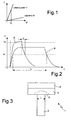
- the resistivity varies by two or more magnitude orders when the material passes from the amorphous phase (more resistive) to the polycrystalline phase (more conductive) and vice versa, as shown in Figure 1. Furthermore, in the amorphous phase, resistivity strongly depends also on temperature, with variations of one magnitude order every 100°C, with a behavior similar to that of P-type semiconductor materials.
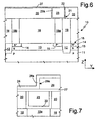
- Phase change may be obtained by locally increasing the temperature, as shown in Figure 2. Below 150°C both phases are stable. Above 200°C (temperature of start of nucleation, designated by T x ), fast nucleation of the crystallites takes place, and, if the material is kept at the crystallization temperature for a sufficient time (time t 2 ), it changes its phase and becomes crystalline. To bring the chalcogenide back into the amorphous state, it is necessary to raise the temperature above the melting temperature T m (approximately 600°C) and then to cool the chalcogenide off rapidly (time t 1 ).
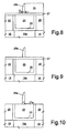
- PCM element 1 which operates according to the principles described above is shown in Figure 3 and comprises a first electrode 2 (of resistive type, forming a heater); a programmable element 3 and a second electrode 5.
- the programmable element 3 is made of a chalcogenide and is normally in the polycrystalline state after processing.
- One part of the programmable element 3 is in direct contact with the first electrode 2 and forms the active portion affected by phase change, hereinafter referred to as the phase change portion 4.
- US-A-6,294,452 discloses a process for forming a contact area of sublithographic dimensions, based on isotropically etching a polysilicon layer. The resulting sublithographic dimensions depend on the quality of the etching.
- US 2001/0002046 discloses a process for forming an electrode of a chalcogenide switching device, wherein a spacer layer deposited in a lithographic opening is anisotropically etched and laterally defines an electrode. The resulting width of the electrode depends on the thickness of a spacer layer.
- European patent application 01128461.9 filed on 5.12.2001, and entitled “Small area contact region, high efficiency phase change memory cell, and manufacturing method thereof", teaches forming the contact area as an intersection of two thin portions extending transversely with respect to one another and each of a sublithographic size. In order to form the thin portions, deposition of layers is adopted.
- any variation in the electrode width L (Figure 3), due for example to the process tolerances, affects, in a linear way, the contact area of the active region 4.
- the width L may have tolerances that are not acceptable as regards repeatability and uniformity of the cell characteristics.
- the object of the invention is thus to provide a contact region having an area less dependent on the process variations.
- an electronic semiconductor device and a process for manufacturing an electronic semiconductor device, as defined respectively in claims 1, and 9.
- the contact area is formed laterally to the active region and has a height and width.
- the height of the contact area is determined by the thickness of a deposited layer, which is technologically controlled and may be designed to be sublithographic.
- the width of the contact area is determined by the width of a spacer which may also be designed of sublithographic dimensions and may be dimensionally controlled with a good accuracy.
- FIG. 4 illustrates the basic structure of a contact structure according to the invention.
- an electronic device 90 has a body 91 (e.g. a substrate) of monocrystalline material defining an upper surface 92 and a lower surface 93 and accommodating electronic components 94, represented schematically.
- a dielectric layer 95 extends on top of the body 91 and accommodates the contact structure, indicated at 98.
- the contact structure 98 is formed by a first electrode 100 and an active region 103 of chalcogenic material.
- the first electrode 100 connected to the electronic components 94 as shown schematically for one of them, has a horizontal portion 102 adjacent to and in contact with the active region 103.
- a second electrode 104 is formed on the active region 103 and is in electric contact therewith.
- the horizontal portion 102 has an elongated shape extending along a longitudinal direction X parallel to the upper and lower surfaces 92, 93 of the body 91.
- the horizontal portion 102 is longitudinally delimited by an end face 110.
- the end face 110 extends in a vertical plane, which is ideally perpendicular to the longitudinal direction X and thus to the upper and lower surfaces 92, 94 and defines a lateral contact area with the active region 103.
- the end face 110 is here rectangular and has a height S (extending parallel to direction Z) and a width W (extending parallel to direction Y).
- the portion of the active region 103 adjacent to the end face 110 undergoes phase change and thus corresponds to the active region 4 of Figure 3.
- the height S is equal to the thickness of the horizontal portion 102 of the first electrode 100, and thus may be designed to be sublithographic, that is smaller than the minimum dimension obtainable through optical UV lithography.
- the contact structure 98 according to Figures 4, 5 is formed by an elongated formation (horizontal portion 102 of the first electrode 100) having a longitudinal extension parallel to the upper surface 92 of the body 91 and an end face 110 extending in a vertical plane and in contact with the active region 103 so that the dimensions of the contact area (defined by the end face 110) are determined by the thickness S of the elongated formation and by the width W thereof.
- the height S of the horizontal portion 102 and thus of the contact area is more controllable than the electrode width L of prior art contact structures ( Figure 3), so that PCM cells having the contact structure of Figure 4 have more uniform dimensions than prior art cells.
- the thickness tolerance of a conductive layer forming the horizontal portion 102 allows, for same overall dimensions, a higher constructive confidence than electrodes the contact area whereof depends on the width L.
- the height S also depends on the quality of the operation used to define the end face 110, in particular by the etching operation used to this end.
- Figure 5 shows the possible variation of the contact area in case etching does not ensure exact verticality of the end face 110, so that horizontal portion 102 has an inclined end face, indicated at 110', forming an angle ⁇ with ideal end face 110 (which, as said, is perpendicular to the upper surface 92).
- width W may be sublithographic, by exploiting the spacer technique, as discussed later on, with reference to Figures 7-12. This technique has a tolerance of ⁇ 10%.
- a wafer 10 comprising a P-type substrate 11 having an upper surface 16 is subjected to standard front end steps.
- insulation regions 12 are formed and delimit active areas; then, in succession, base regions 13 of N-type, base contact regions 14 of N + -type, and emitter regions 15 of P + -type are implanted.
- the base regions 13, base contact regions 14, and emitter regions 15 form diodes or bipolar transistors that define selection elements for the memory cells.
- a first dielectric layer 18 is deposited and planarized; openings are formed in the first dielectric layer 18 above the base contact regions 14 and emitter regions 15, and the openings are filled with tungsten to form emitter contacts 19a and base contacts 19b.
- a second dielectric layer 20 for example, an undoped silicon glass (USG)- is deposited, and openings 21, for example, cylindrical-shaped, are formed in the second dielectric layer 20 above the emitter contact 19a.
- a cup-shaped region 22 is formed, e.g.
- the cup-shaped region 22 thus has a vertical wall 22a extending along the cylindrical side surface of the openings 21.
- a conductive layer 27 (for instance TaSiN, TiSiN, TiN, TiAlN, etc.) having a thickness of 5-50 nm, corresponding to the desired height S of the contact area 110 is deposited, thus obtaining the structure of Figure 6. As visible, the conductive layer 27 extends parallel to the upper surface 16 of substrate 11.
- the width of these stripes has to be enough to ensure that the strips touch the conductive ring formed by the vertical walls 22a on one side and be cut by the trench etch described in Fig.14 on the other side.
- a delimiting layer 29 of insulating material for example oxide
- the delimiting layer 29 has a thickness of, for instance, 20-200 nm.
- one part of the delimiting layer 29 is removed by dry etching to form a step which has a vertical side 29a that extends vertically on top of the dielectric material 23, and crosses the vertical wall 22a of cup-shaped region 22 (at a point located before or behind the drawing plane, and thus not visible in Figure 7).
- a sacrificial layer 28 for example nitride with a thickness of 5-50 nm, is deposited conformally.
- the sacrificial layer 28 forms a vertical wall 28a that extends along the vertical side 29a of the delimiting layer 29.
- the sacrificial layer 31 undergoes an anisotropic etching that results in removal of the horizontal portions of the sacrificial layer 28 and of part of the vertical wall 28a.
- an anisotropic etching that results in removal of the horizontal portions of the sacrificial layer 28 and of part of the vertical wall 28a.
- the remaining portion of the conductive layer 27 (strip-shaped portion 27a) has a height S and a width W.
- an insulating layer 30 e.g. silicon oxide
- an adhesion layer 31 e.g. Si, Ti, Ta, etc.
- a trench 32 of lithographic dimensions is opened.
- the trench 32 is an aperture having a preset length in the direction perpendicular to the drawing sheet, intersects the strip-shaped portion 27a and extends within the second dielectric layer 20 so as to longitudinally delimit the strip-shaped portion 27a.
- the trench 32 determines the length L1 of the strip-shaped portion 27a.
- a chalcogenic layer 33 for example of Ge 2 Sb 2 Te 5 having a thickness of e.g. 20-200 nm, is conformally deposited and fills the trench 32 with a reduced area portion 33b the shape and dimensions whereof are determined by the trench 32.
- a barrier layer 34 for example of Ti/TiN
- a metal layer 35 for example of AlCu
- a barrier layer 34 for example of Ti/TiN
- a metal layer 35 for example of AlCu
- a third dielectric layer 42 is deposited, which is opened above the base contacts 19b. The openings thus formed are filled with tungsten to form top contacts 43 in order to prolong upwards the base contacts 19b.
- standard steps are performed for forming connection lines in contact with the top contacts 43 and with the bits lines 41, pads are formed and a passivation layer 45 is deposited, defining a device main surface 46.
- the strip-shaped portion 27a (corresponding to the horizontal portion 102 of the first electrode 100 of Figure 4) has a longitudinal extension parallel to upper surface 16 of the substrate 11 and forms, with the bottom portion of the reduced area portion 33b, a contact area the height whereof is defined by the thickness of the conductive layer 27 and the width whereof is defined by the thickness of the sacrificial layer 28.
- the quality of the etching of trench 32 determines the orientation of the contact area with respect to the upper surface 16.
- the present contact structure has a very good technological repeatability, a lower dependence from the process variations than prior art solutions, while maintaining a very small contact area, having sublithographic dimensions in both directions.
- the direction of the horizontal portion 102 and the conductive layer 27 is defined with reference to the upper surface 92, 16 of the substrate, intending therewith a plane corresponding to the original upper surface of the wafer.
- the horizontal portion 102 and the conductive layer 27 are perpendicular to the direction of growing of the substrate, due to the deposition of the various superficial layers. If, due to deposition, thermal growing, etching and implant steps carried out on the wafer, the upper surface 16 of the finished device is no more planar, reference may be done to the lower surface 93 of the substrate or to the device main surface 46.
- an alternative embodiment of the present invention provides that the conductive layer 27 is in direct contact with the emitter layer 19a, thus avoiding the dielectric layers 20 and 23 and the cup-shaped region 22.
Landscapes
- Engineering & Computer Science (AREA)
- Manufacturing & Machinery (AREA)
- Semiconductor Memories (AREA)
Abstract
Description
- Figure 1 illustrates the characteristic low field current-voltage of a phase change material;
- Figure 2 shows the temperature versus time plot of a phase change material;
- Figure 3 shows the basic structure of a PCM memory element;
- Figure 4 shows a cross-section of a contact structure according to the present invention;
- Figure 5 is a perspective view of a portion of the contact structure of Figure 4 showing the variability of the contact area due to technological tolerances;
- Figure 6 is a cross-section of a PCM memory element in an initial manufacturing step;
- Figures 7-11 are cross-sections of an enlarged detail of Figure 6, in subsequent manufacturing steps;
- Figure 12 is a perspective view of the structure of Figure 11; and
- Figures 13-16 are cross-sections of the PCM memory element, in subsequent manufacturing steps, taken in a perpendicular plane with respect to Figures 7-11.
Claims (15)
- An electronic semiconductor device (90), comprising:characterized in that said first conducting region (102; 27a) has a strip-like shape having a longitudinal direction delimited by an end face (110) extending transversely to said upper surface (92; 16) and forming a contact area with said second conducting region (103; 33a).a body (91; 11) of semiconductor material having an upper surface (92; 16);a dielectric layer (95; 20, 42) extending on top of said body;a contact structure (98) in said dielectric layer, said contact structure comprising a first conducting region (102; 27a) and a second conducting region (103; 33a), said second conducting region being of chalcogenic material and being in electric contact with said first conducting region;
- A device according to claim 1, wherein said first conducting region (102; 27a) extends in a first direction (X) parallel to said upper surface (92; 16).
- A device according to claim 1 or 2, wherein said end face (110) is perpendicular to said upper surface (92; 16) within process tolerances.
- A device according to any of claims 1-3, wherein said end face (110) has a generally rectangular shape having a height (S) and a width (W).
- A device according to claim 4, wherein said height (S) is comprised between 5 nm and 50 nm and said width (W) is comprised between 5 nm and 50 nm.
- A device according to any of claims 1-4, forming a PCM device including a memory cell comprising a selection element (13-15) and a storage element, said storage element being formed by a heater element (22a, 27a) including said first conducting region (27a) and a storage region (33a) comprising said second conducting region.
- A device according to claim 6, wherein said selection element (13-15) is formed in said body (11), a lower electrode (19a) extends in said dielectric layer (20, 42) between said selection element and said first conducting region (27a) and an upper electrode (35a) extends in said dielectric layer on said second conducting region (33a) and forms a bit line.
- A device according to claim 7, wherein said second conducting region (33a) has a reduced area portion (33b) in contact with said first conducting region (27a) and an upper enlarged portion extending on top of said reduced area portion and in contact with said upper electrode (35a).
- A process for manufacturing an electronic semiconductor device (90), comprising the steps of:characterized in that said step of forming said first conducting region comprises forming a strip-shaped region (102; 27a) having a longitudinal direction delimited by an end face (110) extending transversely to said upper surface (92; 16);providing a body (91; 11) of semiconductor material having an upper surface (92; 16);forming a dielectric layer (95; 20, 42) extending on top of said body; andforming a contact structure (98) in said dielectric layer, said step of forming a contact structure comprising forming a first conducting region (102; 27a) and forming a second conducting region (103; 33a) of chalcogenic material in electric contact with said first conducting region;and said step of forming a second conducting region comprises forming said second conducting region (103; 33a) in contact with said first conducting region at said end face.
- A process according to claim 9, wherein said end face (110) has a generally rectangular shape having a height (S) comprised between 5 nm and 50 nm and a width (W) comprised between 5 nm and 50 nm.
- A process according to claim 9 or 10, wherein said step of forming said first conducting region (27a) comprises depositing a first conductive layer (27) on a bottom portion (20) of said dielectric layer (20, 42); forming a delimitation layer (29) on top of said first conductive layer, said delimitation layer (29) having a step with a vertical side wall surface (29a); forming a sacrificial portion (28a) on said vertical side wall surface; removing said first delimitation layer (29); etching said first conductive layer (27a) using said a sacrificial portion (28a) as a mask; and removing said sacrificial portion.
- A process according to claim 11, wherein said step of forming a sacrificial portion (28a) comprises depositing a sacrificial layer on said first conducting region and said delimitation layer (29) and anisotropically etching said sacrificial layer (28).
- A process according to claim 11 or 12, wherein after removing said sacrificial portion (28a), an insulating layer (30) is deposited on said first conducting region (27a) and said bottom portion of said dielectric layer (20, 42); a trench (32) is formed to remove at least a portion of said bottom portion and an end portion of said first conducting region, thereby defining said end face (110); and a second conductive layer (33) of said chalcogenic material is deposited, filling said trench (32) and contacting said end face (110).
- A process according to claim 13, comprising the step of forming a PCM device including a memory cell comprising a selection element (13-15) and a storage element (33b), said storage element being formed by a heater element including said first conducting region and a storage region comprising said second conducting region.
- A process according to claim 14, comprising, after depositing said second conductive layer (33), depositing an electrode layer (35) and defining said electrode layer and said second conductive layer, to define a bit line (41).
Priority Applications (3)
| Application Number | Priority Date | Filing Date | Title |
|---|---|---|---|
| EP03425016.7A EP1439583B1 (en) | 2003-01-15 | 2003-01-15 | Sublithographic contact structure, in particular for a phase change memory cell, and fabrication process thereof |
| US10/756,195 US7122824B2 (en) | 2003-01-15 | 2004-01-13 | Sublithographic contact structure, in particular for a phase change memory cell, and fabrication process thereof |
| US11/468,153 US7618840B2 (en) | 2003-01-15 | 2006-08-29 | Sublithographic contact structure, in particular for a phase change memory cell, and fabrication process thereof |
Applications Claiming Priority (1)
| Application Number | Priority Date | Filing Date | Title |
|---|---|---|---|
| EP03425016.7A EP1439583B1 (en) | 2003-01-15 | 2003-01-15 | Sublithographic contact structure, in particular for a phase change memory cell, and fabrication process thereof |
Publications (3)
| Publication Number | Publication Date |
|---|---|
| EP1439583A1 true EP1439583A1 (en) | 2004-07-21 |
| EP1439583A9 EP1439583A9 (en) | 2005-03-16 |
| EP1439583B1 EP1439583B1 (en) | 2013-04-10 |
Family
ID=32524297
Family Applications (1)
| Application Number | Title | Priority Date | Filing Date |
|---|---|---|---|
| EP03425016.7A Expired - Lifetime EP1439583B1 (en) | 2003-01-15 | 2003-01-15 | Sublithographic contact structure, in particular for a phase change memory cell, and fabrication process thereof |
Country Status (2)
| Country | Link |
|---|---|
| US (2) | US7122824B2 (en) |
| EP (1) | EP1439583B1 (en) |
Cited By (2)
| Publication number | Priority date | Publication date | Assignee | Title |
|---|---|---|---|---|
| KR100632324B1 (en) | 2004-09-17 | 2006-10-11 | 오보닉스, 아이엔씨. | Phase Change Memory with Ovonic Threshold Switch |
| WO2008127866A1 (en) * | 2007-04-17 | 2008-10-23 | Micron Technology, Inc. | Resistive memory cell fabrication methods and devices |
Families Citing this family (101)
| Publication number | Priority date | Publication date | Assignee | Title |
|---|---|---|---|---|
| US6891747B2 (en) * | 2002-02-20 | 2005-05-10 | Stmicroelectronics S.R.L. | Phase change memory cell and manufacturing method thereof using minitrenches |
| US20060108667A1 (en) | 2004-11-22 | 2006-05-25 | Macronix International Co., Ltd. | Method for manufacturing a small pin on integrated circuits or other devices |
| DE602005011111D1 (en) * | 2005-06-03 | 2009-01-02 | St Microelectronics Srl | Self-aligned process for the production of phase change memory cells |
| US7238994B2 (en) | 2005-06-17 | 2007-07-03 | Macronix International Co., Ltd. | Thin film plate phase change ram circuit and manufacturing method |
| US7394088B2 (en) | 2005-11-15 | 2008-07-01 | Macronix International Co., Ltd. | Thermally contained/insulated phase change memory device and method (combined) |
| US7786460B2 (en) | 2005-11-15 | 2010-08-31 | Macronix International Co., Ltd. | Phase change memory device and manufacturing method |
| US7635855B2 (en) | 2005-11-15 | 2009-12-22 | Macronix International Co., Ltd. | I-shaped phase change memory cell |
| US7414258B2 (en) | 2005-11-16 | 2008-08-19 | Macronix International Co., Ltd. | Spacer electrode small pin phase change memory RAM and manufacturing method |
| US7323357B2 (en) * | 2005-11-17 | 2008-01-29 | Qimonda Ag | Method for manufacturing a resistively switching memory cell and memory device based thereon |
| US7449710B2 (en) | 2005-11-21 | 2008-11-11 | Macronix International Co., Ltd. | Vacuum jacket for phase change memory element |
| US7599217B2 (en) | 2005-11-22 | 2009-10-06 | Macronix International Co., Ltd. | Memory cell device and manufacturing method |
| US7459717B2 (en) | 2005-11-28 | 2008-12-02 | Macronix International Co., Ltd. | Phase change memory cell and manufacturing method |
| US7688619B2 (en) | 2005-11-28 | 2010-03-30 | Macronix International Co., Ltd. | Phase change memory cell and manufacturing method |
| US7531825B2 (en) | 2005-12-27 | 2009-05-12 | Macronix International Co., Ltd. | Method for forming self-aligned thermal isolation cell for a variable resistance memory array |
| US8062833B2 (en) | 2005-12-30 | 2011-11-22 | Macronix International Co., Ltd. | Chalcogenide layer etching method |
| US7560337B2 (en) | 2006-01-09 | 2009-07-14 | Macronix International Co., Ltd. | Programmable resistive RAM and manufacturing method |
| US7741636B2 (en) | 2006-01-09 | 2010-06-22 | Macronix International Co., Ltd. | Programmable resistive RAM and manufacturing method |
| US7432206B2 (en) | 2006-01-24 | 2008-10-07 | Macronix International Co., Ltd. | Self-aligned manufacturing method, and manufacturing method for thin film fuse phase change ram |
| US7351666B2 (en) * | 2006-03-17 | 2008-04-01 | International Business Machines Corporation | Layout and process to contact sub-lithographic structures |
| US7554144B2 (en) | 2006-04-17 | 2009-06-30 | Macronix International Co., Ltd. | Memory device and manufacturing method |
| US7928421B2 (en) * | 2006-04-21 | 2011-04-19 | Macronix International Co., Ltd. | Phase change memory cell with vacuum spacer |
| US7423300B2 (en) * | 2006-05-24 | 2008-09-09 | Macronix International Co., Ltd. | Single-mask phase change memory element |
| US7696506B2 (en) * | 2006-06-27 | 2010-04-13 | Macronix International Co., Ltd. | Memory cell with memory material insulation and manufacturing method |
| US7785920B2 (en) | 2006-07-12 | 2010-08-31 | Macronix International Co., Ltd. | Method for making a pillar-type phase change memory element |
| US7772581B2 (en) | 2006-09-11 | 2010-08-10 | Macronix International Co., Ltd. | Memory device having wide area phase change element and small electrode contact area |
| US7504653B2 (en) | 2006-10-04 | 2009-03-17 | Macronix International Co., Ltd. | Memory cell device with circumferentially-extending memory element |
| US7863655B2 (en) | 2006-10-24 | 2011-01-04 | Macronix International Co., Ltd. | Phase change memory cells with dual access devices |
| US7473576B2 (en) | 2006-12-06 | 2009-01-06 | Macronix International Co., Ltd. | Method for making a self-converged void and bottom electrode for memory cell |
| US7476587B2 (en) | 2006-12-06 | 2009-01-13 | Macronix International Co., Ltd. | Method for making a self-converged memory material element for memory cell |
| US7903447B2 (en) | 2006-12-13 | 2011-03-08 | Macronix International Co., Ltd. | Method, apparatus and computer program product for read before programming process on programmable resistive memory cell |
| US7718989B2 (en) | 2006-12-28 | 2010-05-18 | Macronix International Co., Ltd. | Resistor random access memory cell device |
| US7619311B2 (en) | 2007-02-02 | 2009-11-17 | Macronix International Co., Ltd. | Memory cell device with coplanar electrode surface and method |
| US7884343B2 (en) | 2007-02-14 | 2011-02-08 | Macronix International Co., Ltd. | Phase change memory cell with filled sidewall memory element and method for fabricating the same |
| US7956344B2 (en) | 2007-02-27 | 2011-06-07 | Macronix International Co., Ltd. | Memory cell with memory element contacting ring-shaped upper end of bottom electrode |
| US7699996B2 (en) * | 2007-02-28 | 2010-04-20 | International Business Machines Corporation | Sidewall image transfer processes for forming multiple line-widths |
| US7786461B2 (en) * | 2007-04-03 | 2010-08-31 | Macronix International Co., Ltd. | Memory structure with reduced-size memory element between memory material portions |
| US8610098B2 (en) | 2007-04-06 | 2013-12-17 | Macronix International Co., Ltd. | Phase change memory bridge cell with diode isolation device |
| US7579616B2 (en) * | 2007-04-10 | 2009-08-25 | International Business Machines Corporation | Four-terminal programmable via-containing structure and method of fabricating same |
| US7569844B2 (en) | 2007-04-17 | 2009-08-04 | Macronix International Co., Ltd. | Memory cell sidewall contacting side electrode |
| TWI402980B (en) | 2007-07-20 | 2013-07-21 | Macronix Int Co Ltd | Resistive memory structure with buffer layer |
| US7884342B2 (en) | 2007-07-31 | 2011-02-08 | Macronix International Co., Ltd. | Phase change memory bridge cell |
| US7729161B2 (en) | 2007-08-02 | 2010-06-01 | Macronix International Co., Ltd. | Phase change memory with dual word lines and source lines and method of operating same |
| US8178386B2 (en) | 2007-09-14 | 2012-05-15 | Macronix International Co., Ltd. | Phase change memory cell array with self-converged bottom electrode and method for manufacturing |
| US7642125B2 (en) | 2007-09-14 | 2010-01-05 | Macronix International Co., Ltd. | Phase change memory cell in via array with self-aligned, self-converged bottom electrode and method for manufacturing |
| US7919766B2 (en) | 2007-10-22 | 2011-04-05 | Macronix International Co., Ltd. | Method for making self aligning pillar memory cell device |
| US7646631B2 (en) | 2007-12-07 | 2010-01-12 | Macronix International Co., Ltd. | Phase change memory cell having interface structures with essentially equal thermal impedances and manufacturing methods |
| US7639527B2 (en) | 2008-01-07 | 2009-12-29 | Macronix International Co., Ltd. | Phase change memory dynamic resistance test and manufacturing methods |
| US8338812B2 (en) | 2008-01-16 | 2012-12-25 | Micron Technology, Inc. | Vertical spacer electrodes for variable-resistance material memories and vertical spacer variable-resistance material memory cells |
| US7879643B2 (en) | 2008-01-18 | 2011-02-01 | Macronix International Co., Ltd. | Memory cell with memory element contacting an inverted T-shaped bottom electrode |
| US7879645B2 (en) | 2008-01-28 | 2011-02-01 | Macronix International Co., Ltd. | Fill-in etching free pore device |
| US8158965B2 (en) | 2008-02-05 | 2012-04-17 | Macronix International Co., Ltd. | Heating center PCRAM structure and methods for making |
| US8084842B2 (en) | 2008-03-25 | 2011-12-27 | Macronix International Co., Ltd. | Thermally stabilized electrode structure |
| US8030634B2 (en) | 2008-03-31 | 2011-10-04 | Macronix International Co., Ltd. | Memory array with diode driver and method for fabricating the same |
| US7825398B2 (en) | 2008-04-07 | 2010-11-02 | Macronix International Co., Ltd. | Memory cell having improved mechanical stability |
| US7791057B2 (en) | 2008-04-22 | 2010-09-07 | Macronix International Co., Ltd. | Memory cell having a buried phase change region and method for fabricating the same |
| US8077505B2 (en) | 2008-05-07 | 2011-12-13 | Macronix International Co., Ltd. | Bipolar switching of phase change device |
| US7701750B2 (en) | 2008-05-08 | 2010-04-20 | Macronix International Co., Ltd. | Phase change device having two or more substantial amorphous regions in high resistance state |
| US8415651B2 (en) | 2008-06-12 | 2013-04-09 | Macronix International Co., Ltd. | Phase change memory cell having top and bottom sidewall contacts |
| US8134857B2 (en) | 2008-06-27 | 2012-03-13 | Macronix International Co., Ltd. | Methods for high speed reading operation of phase change memory and device employing same |
| US7932506B2 (en) | 2008-07-22 | 2011-04-26 | Macronix International Co., Ltd. | Fully self-aligned pore-type memory cell having diode access device |
| US7903457B2 (en) | 2008-08-19 | 2011-03-08 | Macronix International Co., Ltd. | Multiple phase change materials in an integrated circuit for system on a chip application |
| US8119528B2 (en) * | 2008-08-19 | 2012-02-21 | International Business Machines Corporation | Nanoscale electrodes for phase change memory devices |
| US7719913B2 (en) | 2008-09-12 | 2010-05-18 | Macronix International Co., Ltd. | Sensing circuit for PCRAM applications |
| US7848139B2 (en) * | 2008-09-18 | 2010-12-07 | Seagate Technology Llc | Memory device structures including phase-change storage cells |
| US8324605B2 (en) | 2008-10-02 | 2012-12-04 | Macronix International Co., Ltd. | Dielectric mesh isolated phase change structure for phase change memory |
| US7897954B2 (en) | 2008-10-10 | 2011-03-01 | Macronix International Co., Ltd. | Dielectric-sandwiched pillar memory device |
| US8036014B2 (en) | 2008-11-06 | 2011-10-11 | Macronix International Co., Ltd. | Phase change memory program method without over-reset |
| US8907316B2 (en) | 2008-11-07 | 2014-12-09 | Macronix International Co., Ltd. | Memory cell access device having a pn-junction with polycrystalline and single crystal semiconductor regions |
| US8664689B2 (en) | 2008-11-07 | 2014-03-04 | Macronix International Co., Ltd. | Memory cell access device having a pn-junction with polycrystalline plug and single-crystal semiconductor regions |
| US7869270B2 (en) | 2008-12-29 | 2011-01-11 | Macronix International Co., Ltd. | Set algorithm for phase change memory cell |
| US8089137B2 (en) | 2009-01-07 | 2012-01-03 | Macronix International Co., Ltd. | Integrated circuit memory with single crystal silicon on silicide driver and manufacturing method |
| US8107283B2 (en) | 2009-01-12 | 2012-01-31 | Macronix International Co., Ltd. | Method for setting PCRAM devices |
| US8030635B2 (en) | 2009-01-13 | 2011-10-04 | Macronix International Co., Ltd. | Polysilicon plug bipolar transistor for phase change memory |
| US8064247B2 (en) | 2009-01-14 | 2011-11-22 | Macronix International Co., Ltd. | Rewritable memory device based on segregation/re-absorption |
| US8933536B2 (en) | 2009-01-22 | 2015-01-13 | Macronix International Co., Ltd. | Polysilicon pillar bipolar transistor with self-aligned memory element |
| US8084760B2 (en) | 2009-04-20 | 2011-12-27 | Macronix International Co., Ltd. | Ring-shaped electrode and manufacturing method for same |
| US8173987B2 (en) | 2009-04-27 | 2012-05-08 | Macronix International Co., Ltd. | Integrated circuit 3D phase change memory array and manufacturing method |
| US8097871B2 (en) | 2009-04-30 | 2012-01-17 | Macronix International Co., Ltd. | Low operational current phase change memory structures |
| US7933139B2 (en) | 2009-05-15 | 2011-04-26 | Macronix International Co., Ltd. | One-transistor, one-resistor, one-capacitor phase change memory |
| US7968876B2 (en) | 2009-05-22 | 2011-06-28 | Macronix International Co., Ltd. | Phase change memory cell having vertical channel access transistor |
| US8350316B2 (en) | 2009-05-22 | 2013-01-08 | Macronix International Co., Ltd. | Phase change memory cells having vertical channel access transistor and memory plane |
| US8809829B2 (en) | 2009-06-15 | 2014-08-19 | Macronix International Co., Ltd. | Phase change memory having stabilized microstructure and manufacturing method |
| US8406033B2 (en) | 2009-06-22 | 2013-03-26 | Macronix International Co., Ltd. | Memory device and method for sensing and fixing margin cells |
| US8238149B2 (en) | 2009-06-25 | 2012-08-07 | Macronix International Co., Ltd. | Methods and apparatus for reducing defect bits in phase change memory |
| US8363463B2 (en) | 2009-06-25 | 2013-01-29 | Macronix International Co., Ltd. | Phase change memory having one or more non-constant doping profiles |
| US7894254B2 (en) | 2009-07-15 | 2011-02-22 | Macronix International Co., Ltd. | Refresh circuitry for phase change memory |
| US8110822B2 (en) | 2009-07-15 | 2012-02-07 | Macronix International Co., Ltd. | Thermal protect PCRAM structure and methods for making |
| US8198619B2 (en) | 2009-07-15 | 2012-06-12 | Macronix International Co., Ltd. | Phase change memory cell structure |
| US8064248B2 (en) | 2009-09-17 | 2011-11-22 | Macronix International Co., Ltd. | 2T2R-1T1R mix mode phase change memory array |
| US8178387B2 (en) | 2009-10-23 | 2012-05-15 | Macronix International Co., Ltd. | Methods for reducing recrystallization time for a phase change material |
| US8729521B2 (en) | 2010-05-12 | 2014-05-20 | Macronix International Co., Ltd. | Self aligned fin-type programmable memory cell |
| US8310864B2 (en) | 2010-06-15 | 2012-11-13 | Macronix International Co., Ltd. | Self-aligned bit line under word line memory array |
| US8728859B2 (en) * | 2010-08-12 | 2014-05-20 | International Business Machines Corporation | Small footprint phase change memory cell |
| US8395935B2 (en) | 2010-10-06 | 2013-03-12 | Macronix International Co., Ltd. | Cross-point self-aligned reduced cell size phase change memory |
| US8497705B2 (en) | 2010-11-09 | 2013-07-30 | Macronix International Co., Ltd. | Phase change device for interconnection of programmable logic device |
| US8467238B2 (en) | 2010-11-15 | 2013-06-18 | Macronix International Co., Ltd. | Dynamic pulse operation for phase change memory |
| US8987700B2 (en) | 2011-12-02 | 2015-03-24 | Macronix International Co., Ltd. | Thermally confined electrode for programmable resistance memory |
| US8861736B2 (en) * | 2012-11-19 | 2014-10-14 | International Business Machines Corporation | Reliable physical unclonable function for device authentication |
| TWI549229B (en) | 2014-01-24 | 2016-09-11 | 旺宏電子股份有限公司 | Multiple phase change materials in a memory device for system on a chip application |
| US9559113B2 (en) | 2014-05-01 | 2017-01-31 | Macronix International Co., Ltd. | SSL/GSL gate oxide in 3D vertical channel NAND |
| US9672906B2 (en) | 2015-06-19 | 2017-06-06 | Macronix International Co., Ltd. | Phase change memory with inter-granular switching |
Citations (1)
| Publication number | Priority date | Publication date | Assignee | Title |
|---|---|---|---|---|
| WO2002009206A1 (en) * | 2000-07-22 | 2002-01-31 | Ovonyx, Inc. | Electrically programmable memory element |
Family Cites Families (30)
| Publication number | Priority date | Publication date | Assignee | Title |
|---|---|---|---|---|
| JP3105770B2 (en) * | 1995-09-29 | 2000-11-06 | 日本電気株式会社 | Method for manufacturing semiconductor device |
| US5814527A (en) | 1996-07-22 | 1998-09-29 | Micron Technology, Inc. | Method of making small pores defined by a disposable internal spacer for use in chalcogenide memories |
| US5789277A (en) | 1996-07-22 | 1998-08-04 | Micron Technology, Inc. | Method of making chalogenide memory device |
| US5998244A (en) | 1996-08-22 | 1999-12-07 | Micron Technology, Inc. | Memory cell incorporating a chalcogenide element and method of making same |
| US5952671A (en) | 1997-05-09 | 1999-09-14 | Micron Technology, Inc. | Small electrode for a chalcogenide switching device and method for fabricating same |
| US6031287A (en) | 1997-06-18 | 2000-02-29 | Micron Technology, Inc. | Contact structure and memory element incorporating the same |
| US20030075778A1 (en) | 1997-10-01 | 2003-04-24 | Patrick Klersy | Programmable resistance memory element and method for making same |
| US6969866B1 (en) | 1997-10-01 | 2005-11-29 | Ovonyx, Inc. | Electrically programmable memory element with improved contacts |
| US6617192B1 (en) | 1997-10-01 | 2003-09-09 | Ovonyx, Inc. | Electrically programmable memory element with multi-regioned contact |
| JPH11168199A (en) | 1997-12-02 | 1999-06-22 | Nippon Steel Corp | Semiconductor memory device and method of manufacturing the same |
| JP3701469B2 (en) | 1998-06-12 | 2005-09-28 | 株式会社ルネサステクノロジ | Manufacturing method of semiconductor integrated circuit device |
| US6750079B2 (en) | 1999-03-25 | 2004-06-15 | Ovonyx, Inc. | Method for making programmable resistance memory element |
| DE60032129T2 (en) | 1999-03-25 | 2007-09-27 | Ovonyx Inc. | ELECTRICALLY PROGRAMMABLE STORAGE ELEMENT WITH IMPROVED CONTACTS |
| US6943365B2 (en) | 1999-03-25 | 2005-09-13 | Ovonyx, Inc. | Electrically programmable memory element with reduced area of contact and method for making same |
| US6238946B1 (en) | 1999-08-17 | 2001-05-29 | International Business Machines Corporation | Process for fabricating single crystal resonant devices that are compatible with integrated circuit processing |
| US6440837B1 (en) | 2000-07-14 | 2002-08-27 | Micron Technology, Inc. | Method of forming a contact structure in a semiconductor device |
| US6313604B1 (en) | 2000-08-01 | 2001-11-06 | Han-Liang Chen | Charging seat for a rechargeable flashlight |
| US6613604B2 (en) | 2001-08-02 | 2003-09-02 | Ovonyx, Inc. | Method for making small pore for use in programmable resistance memory element |
| US6586761B2 (en) | 2001-09-07 | 2003-07-01 | Intel Corporation | Phase change material memory device |
| US6545287B2 (en) | 2001-09-07 | 2003-04-08 | Intel Corporation | Using selective deposition to form phase-change memory cells |
| EP1318552A1 (en) * | 2001-12-05 | 2003-06-11 | STMicroelectronics S.r.l. | Small area contact region, high efficiency phase change memory cell and fabrication method thereof |
| US6512241B1 (en) | 2001-12-31 | 2003-01-28 | Intel Corporation | Phase change material memory device |
| US6891747B2 (en) | 2002-02-20 | 2005-05-10 | Stmicroelectronics S.R.L. | Phase change memory cell and manufacturing method thereof using minitrenches |
| US6972430B2 (en) | 2002-02-20 | 2005-12-06 | Stmicroelectronics S.R.L. | Sublithographic contact structure, phase change memory cell with optimized heater shape, and manufacturing method thereof |
| US6759267B2 (en) * | 2002-07-19 | 2004-07-06 | Macronix International Co., Ltd. | Method for forming a phase change memory |
| US6867425B2 (en) * | 2002-12-13 | 2005-03-15 | Intel Corporation | Lateral phase change memory and method therefor |
| US7205562B2 (en) * | 2002-12-13 | 2007-04-17 | Intel Corporation | Phase change memory and method therefor |
| US6815266B2 (en) * | 2002-12-30 | 2004-11-09 | Bae Systems Information And Electronic Systems Integration, Inc. | Method for manufacturing sidewall contacts for a chalcogenide memory device |
| US7323734B2 (en) | 2003-02-25 | 2008-01-29 | Samsung Electronics Co., Ltd. | Phase changeable memory cells |
| KR100505418B1 (en) * | 2003-04-14 | 2005-08-05 | 주식회사 하이닉스반도체 | Method for forming element isolation film in semiconductor device |
-
2003
- 2003-01-15 EP EP03425016.7A patent/EP1439583B1/en not_active Expired - Lifetime
-
2004
- 2004-01-13 US US10/756,195 patent/US7122824B2/en not_active Expired - Lifetime
-
2006
- 2006-08-29 US US11/468,153 patent/US7618840B2/en not_active Expired - Lifetime
Patent Citations (1)
| Publication number | Priority date | Publication date | Assignee | Title |
|---|---|---|---|---|
| WO2002009206A1 (en) * | 2000-07-22 | 2002-01-31 | Ovonyx, Inc. | Electrically programmable memory element |
Cited By (6)
| Publication number | Priority date | Publication date | Assignee | Title |
|---|---|---|---|---|
| KR100632324B1 (en) | 2004-09-17 | 2006-10-11 | 오보닉스, 아이엔씨. | Phase Change Memory with Ovonic Threshold Switch |
| WO2008127866A1 (en) * | 2007-04-17 | 2008-10-23 | Micron Technology, Inc. | Resistive memory cell fabrication methods and devices |
| US7745231B2 (en) | 2007-04-17 | 2010-06-29 | Micron Technology, Inc. | Resistive memory cell fabrication methods and devices |
| US8193521B2 (en) | 2007-04-17 | 2012-06-05 | Micron Technology, Inc. | Resistive memory cell fabrication methods and devices |
| US8835893B2 (en) | 2007-04-17 | 2014-09-16 | Micron Technology, Inc. | Resistive memory cell fabrication methods and devices |
| US9172040B2 (en) | 2007-04-17 | 2015-10-27 | Micron Technology, Inc. | Resistive memory cell fabrication methods and devices |
Also Published As
| Publication number | Publication date |
|---|---|
| US20060284160A1 (en) | 2006-12-21 |
| US7122824B2 (en) | 2006-10-17 |
| US7618840B2 (en) | 2009-11-17 |
| EP1439583B1 (en) | 2013-04-10 |
| US20040211953A1 (en) | 2004-10-28 |
| EP1439583A9 (en) | 2005-03-16 |
Similar Documents
| Publication | Publication Date | Title |
|---|---|---|
| EP1439583B1 (en) | Sublithographic contact structure, in particular for a phase change memory cell, and fabrication process thereof | |
| US6972430B2 (en) | Sublithographic contact structure, phase change memory cell with optimized heater shape, and manufacturing method thereof | |
| US6891747B2 (en) | Phase change memory cell and manufacturing method thereof using minitrenches | |
| US7514705B2 (en) | Phase change memory cell with limited switchable volume | |
| US7220983B2 (en) | Self-aligned small contact phase-change memory method and device | |
| TWI469268B (en) | Method for forming a memory cell using a gas cluster ion beam | |
| EP2923379B1 (en) | Methods for forming narrow vertical pillars and integrated circuit devices having the same | |
| US7989796B2 (en) | Nonvolatile memory cell with concentric phase change material formed around a pillar arrangement | |
| TWI430488B (en) | Memory device and method of forming same | |
| US7244956B2 (en) | Self-aligned process for manufacturing a phase change memory cell and phase change memory cell thereby manufactured | |
| US7470922B2 (en) | Increasing adherence of dielectrics to phase change materials | |
| CN100379046C (en) | Phase change material memory device and method of forming | |
| US7402455B2 (en) | Manufacturing method of a contact structure and phase change memory cell with elimination of double contacts | |
| US20070145346A1 (en) | Connection electrode for phase change material, associated phase change memory element, and associated production process | |
| WO2011059859A1 (en) | Single crystal phase change material | |
| EP1339103B1 (en) | Sublithographic contact structure, phase change memory cell with optimized heater shape, and manufacturing method thereof | |
| US20060115909A1 (en) | Method for manufacturing a resistively switching memory cell, manufactured memory cell, and memory device based thereon |
Legal Events
| Date | Code | Title | Description |
|---|---|---|---|
| PUAI | Public reference made under article 153(3) epc to a published international application that has entered the european phase |
Free format text: ORIGINAL CODE: 0009012 |
|
| AK | Designated contracting states |
Kind code of ref document: A1 Designated state(s): AT BE BG CH CY CZ DE DK EE ES FI FR GB GR HU IE IT LI LU MC NL PT SE SI SK TR |
|
| AX | Request for extension of the european patent |
Extension state: AL LT LV MK RO |
|
| 17P | Request for examination filed |
Effective date: 20050119 |
|
| AKX | Designation fees paid |
Designated state(s): DE FR GB IT |
|
| RAP1 | Party data changed (applicant data changed or rights of an application transferred) |
Owner name: OVONYX INC. Owner name: STMICROELECTRONICS SRL |
|
| 17Q | First examination report despatched |
Effective date: 20100628 |
|
| RAP1 | Party data changed (applicant data changed or rights of an application transferred) |
Owner name: STMICROELECTRONICS SRL Owner name: OVONYX INC. |
|
| GRAP | Despatch of communication of intention to grant a patent |
Free format text: ORIGINAL CODE: EPIDOSNIGR1 |
|
| GRAS | Grant fee paid |
Free format text: ORIGINAL CODE: EPIDOSNIGR3 |
|
| GRAA | (expected) grant |
Free format text: ORIGINAL CODE: 0009210 |
|
| AK | Designated contracting states |
Kind code of ref document: B1 Designated state(s): DE FR GB IT |
|
| REG | Reference to a national code |
Ref country code: GB Ref legal event code: FG4D |
|
| REG | Reference to a national code |
Ref country code: DE Ref legal event code: R096 Ref document number: 60343719 Country of ref document: DE Effective date: 20130606 |
|
| RAP2 | Party data changed (patent owner data changed or rights of a patent transferred) |
Owner name: STMICROELECTRONICS SRL Owner name: OVONYX INC. |
|
| REG | Reference to a national code |
Ref country code: DE Ref legal event code: R081 Ref document number: 60343719 Country of ref document: DE Owner name: OVONYX INX., US Free format text: FORMER OWNER: STMICROELECTRONICS S.R.L., OVONYX INC., , US Effective date: 20130410 Ref country code: DE Ref legal event code: R081 Ref document number: 60343719 Country of ref document: DE Owner name: OVONYX INX., US Free format text: FORMER OWNER: STMICROELECTRONICS S.R.L., OVONYX INC., , US Effective date: 20130729 Ref country code: DE Ref legal event code: R081 Ref document number: 60343719 Country of ref document: DE Owner name: STMICROELECTRONICS S.R.L., IT Free format text: FORMER OWNER: STMICROELECTRONICS S.R.L., OVONYX INC., , US Effective date: 20130729 Ref country code: DE Ref legal event code: R081 Ref document number: 60343719 Country of ref document: DE Owner name: STMICROELECTRONICS S.R.L., IT Free format text: FORMER OWNER: STMICROELECTRONICS S.R.L., OVONYX INC., , US Effective date: 20130410 Ref country code: DE Ref legal event code: R081 Ref document number: 60343719 Country of ref document: DE Owner name: STMICROELECTRONICS S.R.L., IT Free format text: FORMER OWNERS: STMICROELECTRONICS S.R.L., AGRATE BRIANZA, IT; OVONYX INC., BOISE, ID., US Effective date: 20130729 Ref country code: DE Ref legal event code: R081 Ref document number: 60343719 Country of ref document: DE Owner name: STMICROELECTRONICS S.R.L., IT Free format text: FORMER OWNERS: STMICROELECTRONICS S.R.L., AGRATE BRIANZA, IT; OVONYX INC., BOISE, ID., US Effective date: 20130410 Ref country code: DE Ref legal event code: R081 Ref document number: 60343719 Country of ref document: DE Owner name: OVONYX INX., STERLING HEIGHTS, US Free format text: FORMER OWNERS: STMICROELECTRONICS S.R.L., AGRATE BRIANZA, IT; OVONYX INC., BOISE, ID., US Effective date: 20130729 Ref country code: DE Ref legal event code: R081 Ref document number: 60343719 Country of ref document: DE Owner name: OVONYX INX., STERLING HEIGHTS, US Free format text: FORMER OWNERS: STMICROELECTRONICS S.R.L., AGRATE BRIANZA, IT; OVONYX INC., BOISE, ID., US Effective date: 20130410 Ref country code: DE Ref legal event code: R081 Ref document number: 60343719 Country of ref document: DE Owner name: OVONYX INX., STERLING HEIGHTS, US Free format text: FORMER OWNER: STMICROELECTRONICS S.R.L., OVONYX INC., , US Effective date: 20130410 Ref country code: DE Ref legal event code: R081 Ref document number: 60343719 Country of ref document: DE Owner name: OVONYX INX., STERLING HEIGHTS, US Free format text: FORMER OWNER: STMICROELECTRONICS S.R.L., OVONYX INC., , US Effective date: 20130729 Ref country code: DE Ref legal event code: R081 Ref document number: 60343719 Country of ref document: DE Owner name: STMICROELECTRONICS S.R.L., AGRATE BRIANZA, IT Free format text: FORMER OWNER: STMICROELECTRONICS S.R.L., OVONYX INC., , US Effective date: 20130410 Ref country code: DE Ref legal event code: R081 Ref document number: 60343719 Country of ref document: DE Owner name: STMICROELECTRONICS S.R.L., AGRATE BRIANZA, IT Free format text: FORMER OWNER: STMICROELECTRONICS S.R.L., OVONYX INC., , US Effective date: 20130729 Ref country code: DE Ref legal event code: R081 Ref document number: 60343719 Country of ref document: DE Owner name: OVONYX INX., STERLING HEIGHTS, US Free format text: FORMER OWNERS: STMICROELECTRONICS S.R.L., AGRATE BRIANZA, MAILAND/MILANO, IT; OVONYX INC., BOISE, ID., US Effective date: 20130410 Ref country code: DE Ref legal event code: R081 Ref document number: 60343719 Country of ref document: DE Owner name: STMICROELECTRONICS S.R.L., AGRATE BRIANZA, IT Free format text: FORMER OWNERS: STMICROELECTRONICS S.R.L., AGRATE BRIANZA, MAILAND/MILANO, IT; OVONYX INC., BOISE, ID., US Effective date: 20130729 Ref country code: DE Ref legal event code: R081 Ref document number: 60343719 Country of ref document: DE Owner name: STMICROELECTRONICS S.R.L., AGRATE BRIANZA, IT Free format text: FORMER OWNERS: STMICROELECTRONICS S.R.L., AGRATE BRIANZA, MAILAND/MILANO, IT; OVONYX INC., BOISE, ID., US Effective date: 20130410 Ref country code: DE Ref legal event code: R081 Ref document number: 60343719 Country of ref document: DE Owner name: OVONYX INX., STERLING HEIGHTS, US Free format text: FORMER OWNERS: STMICROELECTRONICS S.R.L., AGRATE BRIANZA, MAILAND/MILANO, IT; OVONYX INC., BOISE, ID., US Effective date: 20130729 |
|
| PLBE | No opposition filed within time limit |
Free format text: ORIGINAL CODE: 0009261 |
|
| STAA | Information on the status of an ep patent application or granted ep patent |
Free format text: STATUS: NO OPPOSITION FILED WITHIN TIME LIMIT |
|
| PG25 | Lapsed in a contracting state [announced via postgrant information from national office to epo] |
Ref country code: IT Free format text: LAPSE BECAUSE OF FAILURE TO SUBMIT A TRANSLATION OF THE DESCRIPTION OR TO PAY THE FEE WITHIN THE PRESCRIBED TIME-LIMIT Effective date: 20130410 |
|
| 26N | No opposition filed |
Effective date: 20140113 |
|
| REG | Reference to a national code |
Ref country code: DE Ref legal event code: R097 Ref document number: 60343719 Country of ref document: DE Effective date: 20140113 |
|
| GBPC | Gb: european patent ceased through non-payment of renewal fee |
Effective date: 20140115 |
|
| REG | Reference to a national code |
Ref country code: FR Ref legal event code: ST Effective date: 20140930 |
|
| PG25 | Lapsed in a contracting state [announced via postgrant information from national office to epo] |
Ref country code: GB Free format text: LAPSE BECAUSE OF NON-PAYMENT OF DUE FEES Effective date: 20140115 Ref country code: FR Free format text: LAPSE BECAUSE OF NON-PAYMENT OF DUE FEES Effective date: 20140131 |
|
| PGFP | Annual fee paid to national office [announced via postgrant information from national office to epo] |
Ref country code: DE Payment date: 20211215 Year of fee payment: 20 |
|
| REG | Reference to a national code |
Ref country code: DE Ref legal event code: R079 Ref document number: 60343719 Country of ref document: DE Free format text: PREVIOUS MAIN CLASS: H01L0027240000 Ipc: H10B0063000000 |
|
| REG | Reference to a national code |
Ref country code: DE Ref legal event code: R071 Ref document number: 60343719 Country of ref document: DE |