EP1439577A2 - Semiconductor device and manufacturing method for the same - Google Patents
Semiconductor device and manufacturing method for the same Download PDFInfo
- Publication number
- EP1439577A2 EP1439577A2 EP03029194A EP03029194A EP1439577A2 EP 1439577 A2 EP1439577 A2 EP 1439577A2 EP 03029194 A EP03029194 A EP 03029194A EP 03029194 A EP03029194 A EP 03029194A EP 1439577 A2 EP1439577 A2 EP 1439577A2
- Authority
- EP
- European Patent Office
- Prior art keywords
- semiconductor substrate
- semiconductor
- hard film
- substrate
- film
- Prior art date
- Legal status (The legal status is an assumption and is not a legal conclusion. Google has not performed a legal analysis and makes no representation as to the accuracy of the status listed.)
- Granted
Links
Images


Classifications
-
- H—ELECTRICITY
- H10—SEMICONDUCTOR DEVICES; ELECTRIC SOLID-STATE DEVICES NOT OTHERWISE PROVIDED FOR
- H10D—INORGANIC ELECTRIC SEMICONDUCTOR DEVICES
- H10D30/00—Field-effect transistors [FET]
- H10D30/60—Insulated-gate field-effect transistors [IGFET]
-
- H—ELECTRICITY
- H10—SEMICONDUCTOR DEVICES; ELECTRIC SOLID-STATE DEVICES NOT OTHERWISE PROVIDED FOR
- H10P—GENERIC PROCESSES OR APPARATUS FOR THE MANUFACTURE OR TREATMENT OF DEVICES COVERED BY CLASS H10
- H10P54/00—Cutting or separating of wafers, substrates or parts of devices
Definitions
- the present invention relates to a semiconductor device and a manufacturing method for the same and, more specifically, to a flexible semiconductor device and a manufacturing method for the same.
- interfaces for directly recognizing images and speech sound such as 3DMDs (see through head mounted display), HDs with a CCD camera built in, headset type glasses and headset type microphones have also been introduced and the market for wearable devices is considered to expand in the future.
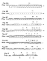
- a substrate with an SOI structure wherein a Si buffer layer 41, a silicon oxide film 42 formed according to a CVD method, a release layer 43 made of a silicon oxide nitride film, and an upper Si layer 44 serving as an element formation layer are laminated in this order on an Si substrate 40 is used and, as shown in Fig. 4B, a pixel portion (pixel region) 44b and a TFT region 44a for an AMLCD are formed on the lamination.
- an oxide film 46 is formed on the pixel portion 44b and the TFT region 44a so as to form an insulator region 45.
- a gate electrode 48 and source/drain regions 49 are formed on the substrate that has been obtained in the above-described manner and, furthermore, this is covered with an insulating film 50 and contact holes and wires 51 are formed on desired regions of the insulating film 50 so as to obtain a TFT 47.
- an opening 52a is formed in a release layer 43 located on the outside of the region that includes the pixel portion 44b and the TFT region 44a and, furthermore, an opening 52b that is greater than the opening 52a is formed in the silicon oxide film 42.
- a support pillar 53 is formed of a silicon oxide film so as to fill in the openings of the silicon oxide film 42 and the release layer 43, an etchant introduction opening 54 is formed in the release layer 43 in a region other than the region that includes the pixel portion 44b and the TFT region 44a surrounded by the support pillar 53, and then an etchant is introduced from this etchant introduction opening 54 so as to remove the silicon oxide film 42 through etching as shown in Fig. 5G and to form a cavity 55.
- the pixel portion 44b and the TFT 47 are placed on the release layer 43 that is supported by the support pillar 53.
- an epoxy resin 56 and a non-photo sensitive transparent resin film 57 are formed on the entirety of the surface of the obtained substrate, and the epoxy resin 56 over the pixel portion 44b and the TFT region 44a is cured by irradiating it with ultraviolet rays while the transparent film 57 which has not been hardened is removed and the support pillar 53 is cut for cleavage, so that a chip in a thin film form is removed.
- circuit elements that include transistors are formed and aligned longitudinally and laterally while an insulating film 60a is formed on a semiconductor substrate 66 wherein no electrodes are formed.
- a semiconductor substrate 66 is polished so as to reduce the thickness of the wafer to a predetermined thickness.
- trenches 62 having a cross-section in the V-form are formed longitudinally and laterally along division lines (scribe area) for dividing the circuit elements on the surface of the semiconductor substrate 66.
- insulating film 60b is formed on the semiconductor substrate 66 so as to cover the surfaces of the trenches 62 and, as shown in Fig. 6E, the insulating film 60b on the surface of the semiconductor substrate 66 is selectively removed so as to expose the surface of the semiconductor substrate 66 and then an electrode is formed on the surface of the semiconductor substrate 66 and a bump is formed on this electrode so as to obtain a bump electrode (protruding electrode) 65.
- a tape 63 for polishing is adhered to the entire surface of the semiconductor substrate 66 by means of an adhesive 64 and, as shown in Fig. 6G, the bottom surface of the semiconductor substrate 66 is polished until the bottoms of the trenches 62 are exposed.
- the semiconductor substrate 66 is divided in the condition that the semiconductor substrate 66 is adhered to the tape 63 for polishing, so that semiconductor chips are formed.
- the tape 63 for polishing and the adhesive 64 are peeled off and an insulating film 60c is formed on the bottom surface of each semiconductor chip as shown in Fig. 6I.
- an SOI substrate since an SOI substrate is used, the cost of the substrate itself is high, and the already existing technology for designing and processing semiconductor devices in bulk substrates cannot be utilized.
- an upper Si layer 44 which is an element formation layer, is deposited directly on the release layer 43; therefore, there is a possibility in that the upper Si layer 44 peels off during the element formation process due to a problem concerning adhesiveness between the upper Si layer 44 and the release layer 43 (adhesiveness depends on the surface form of the lower release layer), leading to a problem of a lack of flexibility due to the relative unevenness of the film thickness of the upper Si layer 44.
- the film thickness of the semiconductor layer is determined by the film thickness of the upper Si layer 44 on the SOI substrate; therefore, a problem arises wherein the film thickness cannot be freely set so that the semiconductor layer exhibits a desired flexibility and light transmission.
- the insulating film that serves as a stopper exists inside of the V-form trenches; therefore, there is a possibility of causing unevenness of the film thickness or cracks in the substrate due to stress being concentrated on the bottom of the V-form trenches resulting in a lack of control when polishing the substrate. Therefore, a problem arises wherein the film thickness cannot be freely set so that the semiconductor layer exhibits a desired flexibility and light transmission.
- the present invention has been made to solve such problems and an object of the present invention is to provide a semiconductor device and a manufacturing method for the same, wherein flexibility and light transmission can be provided to a chip itself in a thin film form.
- the present invention provides a semiconductor device comprising a semiconductor substrate providing a semiconductor element and a hard film which covers a part or the entirety of a side of the semiconductor substrate and which has top and bottom surfaces in approximately the same planes as those of the top and bottom surfaces of the semiconductor substrate, wherein the side of the semiconductor substrate covered with the hard film is processed so as to be perpendicular or substantially perpendicular to the surface of the semiconductor substrate.
- the present invention also provides a manufacturing method for a semiconductor device, comprising the steps of:
- a semiconductor device of the present invention is mainly comprises a semiconductor substrate and a hard film that covers at least a part of a side of the semiconductor substrate.
- the semiconductor substrate is not particularly limited as long as it is one of the types that are conventionally utilized for semiconductor devices, and examples thereof include substrates of element semiconductors such as silicon and germanium; substrates of compound semiconductors such as GaAs, InGaAs and ZnSe; epitaxial substrates wherein epitaxial layers of the above semiconductors are formed on semiconductor substrates so as to have a thickness of, for example, approximately 1 ⁇ m; and substrates where semiconductor layers are formed on insulating substrates such as of glass and plastic.
- a single crystal or polycrystal silicon substrate is preferable.
- Element isolation regions, elements such as transistors, capacitors and resisters, interlayer insulating films and circuits made of combinations thereof may be formed in a single or multiple layer structure on the semiconductor substrate.
- impurities may be doped so that the resistance of the semiconductor substrate is set at a predetermined value.
- the film thickness of the semiconductor substrate is not particularly limited, it is preferable for the film thickness to allow the substrate to bend in accordance with the material thereof in the case where stress is applied to the substrate, that is, to allow the substrate to secure a so-called flexibility and/or it is preferable for the film thickness to allow the substrate to exhibit light transmission.
- an example of the film thickness includes in a range from approximately 1 to 60 ⁇ m.
- a part or the entirety of a side of the semiconductor substrate is covered with the hard film, which will be described later, and it is necessary for the side that is covered with the hard film to be perpendicular or substantially perpendicular to the surface of the semiconductor substrate.
- substantially perpendicular indicates the state of being substantially perpendicular, forming approximately 90° ⁇ 5°, to the surface of the semiconductor substrate.
- the material of the hard film is not particularly limited as long as it has an etching or polishing rate lower than that of the semiconductor substrate, it is preferable for the hard film to be made of an insulating material. Specific examples thereof include a silicon oxide film, a silicon nitride film and a lamination thereof.
- the hard film covers a part or the entirety of a side of the semiconductor substrate and "a part" in this case indicates a part of the outer periphery of the semiconductor substrate and does not indicate a part in the thickness direction. That is, it is suitable for the hard film that covers a side of the semiconductor substrate to have top and bottom surfaces being in approximately the same planes with the top and bottom surfaces, respectively, of the semiconductor substrate in the covering portion.
- the film thickness of the hard film is suitable for the film thickness of the hard film to coincide with the film thickness of the semiconductor substrate. It is necessary to form the hard film so that the hard film has a width to a degree that the flexibility of the semiconductor substrate is not excessively lost and it is suitable for the width of the hard film to be from approximately 50 to 200 ⁇ m in the longitudinal direction or in the lateral direction of the surface of the semiconductor substrate.
- a through hole may be formed in the hard film and a through electrode may be formed by filling the inside of the through hole with a conductive material.
- the film thickness of the through electrode coincides with the film thicknesses of the semiconductor substrate and of the hard film and, accordingly, it is suitable for the through electrode has top and bottom surfaces which are in approximately the same planes as those of the top and bottom surfaces, respectively, of the semiconductor substrate and of the hard film.
- the conductive material forming the through electrode is not particularly limited as long as it is a conductive material that can be utilized for a conventional electrode, and examples thereof include amorphous, single crystal or polycrystal N-type or P-type element semiconductors (e.g., silicon or germanium) or compound semiconductors (e.g., GaAs, InP, ZnSe, CsS); metals such as gold, platinum, silver, copper and aluminum; a high melting point metal such as titanium, tantalum and tungsten; single layer films or multilayer films of silicide or polycide of the high melting point metal. In particular, the high melting point metal is preferable.
- the size of the through hole can be appropriately adjusted in accordance with the size (width in the direction perpendicular to the direction of the length of the hard film) of the hard film.
- a recess is formed in a region of a semiconductor substrate, where a semiconductor element is formed, on the semiconductor substrate so as not to be located in the region and the recess is perpendicular to the surface of the semiconductor substrate in step (a).
- the recess can be formed as a hole that does not penetrate or as a trench according to a method well known in the art such as photolithography and an etching process.
- the depth of the recess can be appropriately adjusted in accordance with the thickness of the semiconductor substrate to be obtained taking flexibility and/or light transmission into consideration as described above, and the depth includes a range from approximately 1 to 60 ⁇ m.
- the bottom of the recess is parallel to the surface of the semiconductor substrate.
- the recess can be formed in the entirety or in a part of the region such as of scribe lines where no semiconductor element are formed. Although only one recess may be formed in the semiconductor substrate, it is preferable to form a plurality of recesses. Although it is appropriate for all of the recesses to have the same depth in the case where a plurality of recesses is formed, it is unnecessary for the recesses to have the same size (length, width or diameter in the plane direction of the substrate).
- the recess is filled in with a hard film in step (b).
- the filling of the hard film can be implemented according to a method well known in the art, for example, by forming a hard film on the entire surface of the semiconductor substrate that includes the recess so as to have a film thickness greater than the depth of the recess by means of a sputtering method, a CVD method, a deposition method or the like, and by etching or polishing the formed hard film until the surface of the semiconductor substrate is exposed.
- the etching may be either wet etching or dry etching and a CMP method and the like can used as the polishing.
- the surface of the hard film can be made to be approximately in the same plane with the surface of the semiconductor substrate.
- a through electrode may be formed in the hard film by forming a through hole in the hard film after the hard film has been filled in the recess and by filling in this through hole with a conductive material.
- the through hole can be formed to have a desired size according to a method well known in the art such as photolithography and an etching process.
- the filling of the conductive material into the through hole can be carried out according to the same method as that for filling in the recess with the hard film as described above.
- a support substrate is adhered to the surface of the semiconductor substrate, which includes the recess, in step (c).
- the support substrate may be made of any material and may have any film thickness as long as it can provide the strength for preventing the occurrence of cracks or the like in the semiconductor substrate at the time when the bottom surface of the semiconductor substrate is made to retrogress until the bottom surface of the hard film is exposed in a manner which will be described later.
- Specific examples of the support substrate include a variety of substrates of metal, plastic, glass, wood, semiconductor and the like.
- the adhesion may be carried out in a manner such that the semiconductor substrate can be firmly adhered to the support substrate using adhesive, an adhesive tape or the like, thereby cracks in the semiconductor substrate can be prevented from occurring at the time when the semiconductor substrate is converted into a thin film as described below.
- the semiconductor substrate is made to retrogress from the bottom surface side until the bottom surface of the hard film is exposed.
- the retrogression of the semiconductor substrate can be carried out by means of etching or polishing as described above. That is, the hard film has an etching rate or a polishing rate lower than that of the semiconductor substrate, so that the hard film becomes a stopper for the etching or polishing in the case where the semiconductor substrate is retrogressed from the bottom surface and, accordingly, the semiconductor substrate can be converted to a thin film having desired film thickness by retrogressing the semiconductor substrate until the bottom surface of the hard film is exposed wherein the retrogression of the semiconductor substrate does not proceed beyond the depth of the predetermined recesses and, in addition, the bottom surface of the hard film can be made in the same plane as the bottom surface of the semiconductor substrate.
- step (d) the hard film is cut in the region where the hard film is formed, thereby the semiconductor substrate is divided into pieces.
- the division herein is referred to as a so-called dicing and the semiconductor substrate can be divided into semiconductor chips by cutting the hard film, that is, by arbitrarily cutting the semiconductor substrate itself. It is noted that this dicing may be carried out in the state where the support substrate is adhered to the semiconductor substrate and, after that, the support substrate may be removed, or the dicing may be carried out after the removal of the support substrate.
- the semiconductor device according to the present invention is a semiconductor device having so-called flexibility and light transmission and, therefore, can be used in the modes where flexibility and light transmission are particularly required.
- a variety of applications such as a liquid crystal panel, a memory card and an IC card are included in the modes.
- it may be used in an application wherein no flexibility or no light transmission is particularly required.
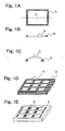
- a semiconductor device of Embodiment 1 is a semiconductor chip formed of an element portion A and a hard film portion B that covers a part or the entirety of the periphery of the element portion A as shown in Figs. 1A and 1B.
- the element portion A which is flexible, is formed of transistors, capacitors, resisters or a combination thereof on a silicon substrate having a film thickness of approximately 30 ⁇ m and a size of 1 mm ⁇ 2 mm. At least the sides of the silicon substrate covered with the hard film portion B are perpendicular or substantially perpendicular to the surface of the silicon substrate.
- the hard film portion B is formed of an insulating film, for example, a silicon oxide film so as to have a width of approximately 50 ⁇ m, and covers a part or the entirety of the periphery of the element portion A as shown in Figs. 1D and 1E.
- an insulating film for example, a silicon oxide film so as to have a width of approximately 50 ⁇ m, and covers a part or the entirety of the periphery of the element portion A as shown in Figs. 1D and 1E.
- Such a semiconductor chip can be formed according to the following manufacturing method.
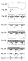
- semiconductor elements are formed on a p-type silicon substrate 11 having an impurity concentration of approximately 5 ⁇ 10 15 cm -3 .
- the sides of the recesses 12 are processed so as to be substantially perpendicular to the surface of the silicon substrate 11.
- a silicon oxide film 13 is formed on the entirety of the surface of the silicon substrate 11 that includes the recesses 12 according to a plasma CVD method and the silicon oxide film is polished according to a CMP method until the surface of the silicon substrate 11 is exposed, so that the silicon oxide film 13 is filled into recesses 12.
- the polishing by means of CMP may be stopped as shown in Fig. 2C' before the surface of the silicon substrate 11 is exposed so that the silicon oxide film 13 remains on the entirety of the surface of the silicon substrate 11 so as to be used as a protective film at the time when a support substrate 14 is adhered to the silicon substrate.
- the support substrate 14 made of Al is adhered to the silicon substrate 11 from the recess 12 side, into which the silicon oxide film 13 has been filled, by using for example adhesive and the bottom surface of the silicon substrate 11 is polished as shown in Fig. 2E until the silicon oxide film 13 is exposed, so that the silicon substrate 11 is converted into a thin film as shown in Fig. 2F.
- the silicon oxide film 13 has a polishing ratio lower than that of silicon substrate 11 so as to become a stopper for polishing; therefore, the polishing does not proceed beyond the predetermined depth of the recesses 12, so that the silicon substrate 11 having a desired film thickness can be obtained.
- the support substrate 14 is removed from the silicon substrate 11 and dicing is carried out on the portion of the silicon oxide film 13 as shown in Fig. 2H, thereby chips forming semiconductor devices are obtained from the silicon substrate 11.
- the obtained semiconductor chips are flexible semiconductor chips wherein the end portions thereof are covered with the hard film portions and are bent by pressure applied in one direction so as not to be broken as shown in Fig. 1C.
- the semiconductor chip can stably operate because of the flexibility of the semiconductor chip itself even when some stress is applied to the liquid crystal panel.
- a semiconductor device of this Embodiment 2 is substantially the same as Embodiment 1 except for the formation of through holes in the hard film portion B and the formation of a through electrode made of tungsten inside of the hole.
- Such a semiconductor chip can be formed according to the manufacturing method which will be described later.
- the recesses 12 are formed in the silicon substrate 11 wherein semiconductor element (not shown) have been formed so that the sides of the recesses 12 become approximately perpendicular to the surface of the silicon substrate 11 are in the same manner as in Embodiment 1.
- the recesses 12 are filled in with the silicon oxide film 13 in the same manner as in Embodiment 1. After that, through holes are formed in a part of the silicon oxide film 13 by means of photolithographic and etching processes. Then, the through holes are selectively filled in with tungsten so as to form through electrodes 15.
- the support substrate 14 is adhered to the silicon substrate 11 in the same manner as in Embodiment 1. and the silicon substrate 11 is converted into a thin film and the support substrate 14 is peeled off followed by dicing, so that semiconductor chips are obtained.
- the obtained semiconductor chips are flexible chips wherein the end portions thereof are covered with hard film portions; therefore, a semiconductor chip is mounted on for example, a plastic liquid crystal panel and can stably operate even when stress is applied to the liquid crystal panel.
- the present invention provides a semiconductor device comprising: a semiconductor substrate where a semiconductor element is formed on a surface; and a hard film which covers a part or the entirety of a side of this semiconductor substrate and which has top and bottom surfaces in approximately the same planes with the top and bottom surfaces of the semiconductor substrate, wherein the side of the semiconductor substrate covered with the hard film is processed so as to be perpendicular or substantially perpendicular to the surface of the semiconductor substrate; therefore, a high quality semiconductor device having appropriate strength in addition to flexibility and / or light transmission can be provided for implementing high performance. Accordingly, it becomes possible to apply a semiconductor substrate according to the present invention in a foldable, wearable computer or in a display such as liquid crystal displays having light transmission as system package solution that corresponds to miniaturized and portable devices.
- a bulk substrate can be used in place of an SOI substrate; therefore, the substrate itself is inexpensive and the already existing technology for designing and processing semiconductor devices in bulk substrates can be utilized and it becomes possible to lower the total cost from development to production.
- a semiconductor device can be manufactured in a simple process in comparison with the case where an SOI substrate is used, and in addition, recesses are formed perpendicular to the semiconductor substrate where a hard film is placed in the recesses; therefore, the hard film can be made to function as a stopper or a protective film at the time of retrogression of the semiconductor substrate, for example, at the time of polishing and unevenness of the film thickness and cracks can be prevented from occurring without causing concentration of stress, so that it becomes possible to reduce the manufacturing cost and to increase yield.
Landscapes
- Internal Circuitry In Semiconductor Integrated Circuit Devices (AREA)
- Thin Film Transistor (AREA)
- Element Separation (AREA)
- Recrystallisation Techniques (AREA)
- Bipolar Transistors (AREA)
- Dicing (AREA)
Abstract
Description
Claims (7)
- A semiconductor device, comprising:wherein the side of the semiconductor substrate covered with the hard film is processed so as to be perpendicular or substantially perpendicular to the surface of the semiconductor substrate.a semiconductor substrate providing a semiconductor element ; anda hard film which covers a part or the entirety of a side of the semiconductor substrate and which has top and bottom surfaces in approximately the same planes as those of the top and bottom surfaces of the semiconductor substrate,
- The device of claim 1, wherein the hard film provides a through hole and a through electrode is formed in the through hole so that the through electrode has top and bottom surfaces which are in approximately the same planes as those of the top and bottom surfaces of the hard film.
- The device of claim 1, wherein the semiconductor substrate is a silicon substrate.
- The device of claim 1, wherein the hard film is a silicon oxide film or a silicon nitride film.
- The device of claim 2, wherein the through electrode is formed of a high melting point metal.
- A manufacturing method for a semiconductor device, comprising the steps of:(a) forming a recess in a semiconductor substrate, the semiconductor substrate having a semiconductor element, the recess being located in a region of the semiconductor substrate where the semiconductor element is not formed, the recess is being perpendicular to a surface of the semiconductor substrate;(b) filling the recess with a material of a hard film;(c) adhering a support substrate to the surface of the semiconductor substrate, the surface includes the recess, and making the bottom surface of the semiconductor substrate retrogress until a bottom surface of the hard film is exposed; and(d) dividing the semiconductor substrate into pieces by cutting the hard film.
- The manufacturing method for a semiconductor device according to claim 6, wherein in the step (b), filling the recess with a material of a hard film is followed by forming a through hole in the hard film and filling the through hole with a conductive material to form a through electrode.
Applications Claiming Priority (2)
| Application Number | Priority Date | Filing Date | Title |
|---|---|---|---|
| JP2003003413 | 2003-01-09 | ||
| JP2003003413A JP2004221125A (en) | 2003-01-09 | 2003-01-09 | Semiconductor device and manufacturing method thereof |
Publications (3)
| Publication Number | Publication Date |
|---|---|
| EP1439577A2 true EP1439577A2 (en) | 2004-07-21 |
| EP1439577A3 EP1439577A3 (en) | 2004-08-25 |
| EP1439577B1 EP1439577B1 (en) | 2006-08-16 |
Family
ID=32588480
Family Applications (1)
| Application Number | Title | Priority Date | Filing Date |
|---|---|---|---|
| EP03029194A Expired - Lifetime EP1439577B1 (en) | 2003-01-09 | 2003-12-18 | Semiconductor device and manufacturing method for the same |
Country Status (7)
| Country | Link |
|---|---|
| US (1) | US7033863B2 (en) |
| EP (1) | EP1439577B1 (en) |
| JP (1) | JP2004221125A (en) |
| KR (1) | KR100582485B1 (en) |
| CN (1) | CN1314077C (en) |
| DE (1) | DE60307589T2 (en) |
| TW (1) | TWI256682B (en) |
Cited By (3)
| Publication number | Priority date | Publication date | Assignee | Title |
|---|---|---|---|---|
| FR2969376A1 (en) * | 2010-12-16 | 2012-06-22 | St Microelectronics Crolles 2 | PROCESS FOR PRODUCING INTEGRATED CIRCUIT CHIPS |
| US8466038B2 (en) | 2010-12-16 | 2013-06-18 | Stmicroelectronics (Crolles 2) Sas | Process for fabricating integrated-circuit chips |
| DE102015114304B4 (en) | 2014-09-04 | 2021-08-19 | Infineon Technologies Austria Ag | A method of manufacturing a semiconductor device, semiconductor device and semiconductor component |
Families Citing this family (7)
| Publication number | Priority date | Publication date | Assignee | Title |
|---|---|---|---|---|
| JP4501633B2 (en) * | 2004-10-28 | 2010-07-14 | ソニー株式会社 | Solid-state imaging device and manufacturing method thereof |
| JP2008233779A (en) * | 2007-03-23 | 2008-10-02 | Bridgestone Corp | Flexible electronic device |
| CN102637788B (en) * | 2008-06-02 | 2014-06-25 | 香港应用科技研究院有限公司 | Semiconductor wafer and semiconductor device |
| US20140374151A1 (en) * | 2013-06-24 | 2014-12-25 | Jia Lin Yap | Wire bonding method for flexible substrates |
| US9287236B2 (en) | 2014-07-17 | 2016-03-15 | Freescale Semiconductor, Inc. | Flexible packaged integrated circuit |
| DE102017102127B4 (en) * | 2017-02-03 | 2023-03-09 | Infineon Technologies Ag | Method of manufacturing semiconductor devices using epitaxy and semiconductor devices with a lateral structure |
| JP7807218B2 (en) * | 2021-12-03 | 2026-01-27 | 株式会社ディスコ | Grinding method for workpiece |
Family Cites Families (20)
| Publication number | Priority date | Publication date | Assignee | Title |
|---|---|---|---|---|
| US5071792A (en) * | 1990-11-05 | 1991-12-10 | Harris Corporation | Process for forming extremely thin integrated circuit dice |
| US5376561A (en) * | 1990-12-31 | 1994-12-27 | Kopin Corporation | High density electronic circuit modules |
| JPH0574776A (en) * | 1991-09-13 | 1993-03-26 | Hitachi Ltd | Mounting structure of semiconductor device |
| DE4317721C1 (en) * | 1993-05-27 | 1994-07-21 | Siemens Ag | Process for separating chips from a wafer |
| US5691248A (en) * | 1995-07-26 | 1997-11-25 | International Business Machines Corporation | Methods for precise definition of integrated circuit chip edges |
| JPH10223626A (en) | 1997-02-12 | 1998-08-21 | Hitachi Ltd | Semiconductor chip, method of manufacturing semiconductor chip, semiconductor device, electronic device |
| US5863813A (en) * | 1997-08-20 | 1999-01-26 | Micron Communications, Inc. | Method of processing semiconductive material wafers and method of forming flip chips and semiconductor chips |
| US6187677B1 (en) * | 1997-08-22 | 2001-02-13 | Micron Technology, Inc. | Integrated circuitry and methods of forming integrated circuitry |
| JP4187808B2 (en) * | 1997-08-25 | 2008-11-26 | 株式会社ルネサステクノロジ | Manufacturing method of semiconductor device |
| US6204146B1 (en) * | 1998-12-10 | 2001-03-20 | United Microelectronics Corp. | Method of fabricating shallow trench isolation |
| JP2000269166A (en) * | 1999-03-15 | 2000-09-29 | Toshiba Corp | Method of manufacturing integrated circuit chip and semiconductor device |
| JP3792954B2 (en) * | 1999-08-10 | 2006-07-05 | 株式会社東芝 | Manufacturing method of semiconductor device |
| JP3455762B2 (en) * | 1999-11-11 | 2003-10-14 | カシオ計算機株式会社 | Semiconductor device and manufacturing method thereof |
| JP2001144173A (en) * | 1999-11-17 | 2001-05-25 | Denso Corp | Method for manufacturing semiconductor device |
| US6524890B2 (en) * | 1999-11-17 | 2003-02-25 | Denso Corporation | Method for manufacturing semiconductor device having element isolation structure |
| JP2001313350A (en) * | 2000-04-28 | 2001-11-09 | Sony Corp | Chip-shaped electronic component, method for manufacturing the same, pseudo wafer used for the manufacture thereof, and method for manufacturing the same |
| JP2002198463A (en) * | 2000-12-26 | 2002-07-12 | Canon Inc | Chip size package and manufacturing method thereof |
| US6525407B1 (en) * | 2001-06-29 | 2003-02-25 | Novellus Systems, Inc. | Integrated circuit package |
| JP4316186B2 (en) | 2002-04-05 | 2009-08-19 | シャープ株式会社 | Semiconductor device and manufacturing method thereof |
| US6649445B1 (en) * | 2002-09-11 | 2003-11-18 | Motorola, Inc. | Wafer coating and singulation method |
-
2003
- 2003-01-09 JP JP2003003413A patent/JP2004221125A/en active Pending
- 2003-12-11 US US10/732,814 patent/US7033863B2/en not_active Expired - Fee Related
- 2003-12-15 TW TW092135437A patent/TWI256682B/en not_active IP Right Cessation
- 2003-12-18 DE DE60307589T patent/DE60307589T2/en not_active Expired - Lifetime
- 2003-12-18 EP EP03029194A patent/EP1439577B1/en not_active Expired - Lifetime
- 2003-12-19 KR KR1020030093629A patent/KR100582485B1/en not_active Expired - Fee Related
-
2004
- 2004-01-09 CN CNB2004100015145A patent/CN1314077C/en not_active Expired - Fee Related
Cited By (4)
| Publication number | Priority date | Publication date | Assignee | Title |
|---|---|---|---|---|
| FR2969376A1 (en) * | 2010-12-16 | 2012-06-22 | St Microelectronics Crolles 2 | PROCESS FOR PRODUCING INTEGRATED CIRCUIT CHIPS |
| US8466038B2 (en) | 2010-12-16 | 2013-06-18 | Stmicroelectronics (Crolles 2) Sas | Process for fabricating integrated-circuit chips |
| US8518802B2 (en) | 2010-12-16 | 2013-08-27 | Stmicroelectronics (Crolles 2) Sas | Process for fabricating integrated-circuit chips |
| DE102015114304B4 (en) | 2014-09-04 | 2021-08-19 | Infineon Technologies Austria Ag | A method of manufacturing a semiconductor device, semiconductor device and semiconductor component |
Also Published As
| Publication number | Publication date |
|---|---|
| KR20040064209A (en) | 2004-07-16 |
| DE60307589D1 (en) | 2006-09-28 |
| US7033863B2 (en) | 2006-04-25 |
| EP1439577A3 (en) | 2004-08-25 |
| EP1439577B1 (en) | 2006-08-16 |
| CN1314077C (en) | 2007-05-02 |
| TWI256682B (en) | 2006-06-11 |
| JP2004221125A (en) | 2004-08-05 |
| US20040137720A1 (en) | 2004-07-15 |
| KR100582485B1 (en) | 2006-05-22 |
| DE60307589T2 (en) | 2007-08-09 |
| CN1518059A (en) | 2004-08-04 |
| TW200416836A (en) | 2004-09-01 |
Similar Documents
| Publication | Publication Date | Title |
|---|---|---|
| US7898070B2 (en) | Image sensor package and fabrication method thereof | |
| EP1391923B1 (en) | Manufacturing method of semiconductor device | |
| US7482251B1 (en) | Etch before grind for semiconductor die singulation | |
| KR100589570B1 (en) | Method for manufacturing semiconductor device | |
| EP1391924A1 (en) | Semiconductor device and its manufacturing method, circuit board, and electric apparatus | |
| US8624383B2 (en) | Integrated circuit package and method for fabrication thereof | |
| US8232202B2 (en) | Image sensor package and fabrication method thereof | |
| JP4101643B2 (en) | Method for manufacturing semiconductor device | |
| JP5866086B2 (en) | Method for manufacturing semiconductor device | |
| CN107681000B (en) | Electronic device and method of forming the same | |
| EP1439577B1 (en) | Semiconductor device and manufacturing method for the same | |
| EP1453090A3 (en) | Manufacturing method of semiconductor device | |
| US7655539B2 (en) | Dice by grind for back surface metallized dies | |
| US6888234B2 (en) | Semiconductor device and manufacturing method for the same | |
| US20060068534A1 (en) | Method for manufacturing semiconductor device | |
| WO2007069456A1 (en) | Semiconductor device manufacturing method | |
| US6762804B2 (en) | Reflective-type liquid crystal display and method for manufacturing the same | |
| US20040140469A1 (en) | Panel of a flat display and method of fabricating the panel | |
| US20220208724A1 (en) | Method for semi-wafer level packaging | |
| JP2003318221A (en) | Method for manufacturing semiconductor device | |
| JP2005039014A (en) | Semiconductor device and manufacturing method thereof | |
| JP2010021258A (en) | Semiconductor device and its manufacturing method |
Legal Events
| Date | Code | Title | Description |
|---|---|---|---|
| PUAI | Public reference made under article 153(3) epc to a published international application that has entered the european phase |
Free format text: ORIGINAL CODE: 0009012 |
|
| PUAL | Search report despatched |
Free format text: ORIGINAL CODE: 0009013 |
|
| AK | Designated contracting states |
Kind code of ref document: A2 Designated state(s): AT BE BG CH CY CZ DE DK EE ES FI FR GB GR HU IE IT LI LU MC NL PT RO SE SI SK TR |
|
| AX | Request for extension of the european patent |
Extension state: AL LT LV MK |
|
| AK | Designated contracting states |
Kind code of ref document: A3 Designated state(s): AT BE BG CH CY CZ DE DK EE ES FI FR GB GR HU IE IT LI LU MC NL PT RO SE SI SK TR |
|
| AX | Request for extension of the european patent |
Extension state: AL LT LV MK |
|
| 17P | Request for examination filed |
Effective date: 20041124 |
|
| 17Q | First examination report despatched |
Effective date: 20050224 |
|
| AKX | Designation fees paid |
Designated state(s): DE FR |
|
| RBV | Designated contracting states (corrected) |
Designated state(s): DE FR |
|
| GRAP | Despatch of communication of intention to grant a patent |
Free format text: ORIGINAL CODE: EPIDOSNIGR1 |
|
| GRAS | Grant fee paid |
Free format text: ORIGINAL CODE: EPIDOSNIGR3 |
|
| GRAA | (expected) grant |
Free format text: ORIGINAL CODE: 0009210 |
|
| AK | Designated contracting states |
Kind code of ref document: B1 Designated state(s): DE FR |
|
| REF | Corresponds to: |
Ref document number: 60307589 Country of ref document: DE Date of ref document: 20060928 Kind code of ref document: P |
|
| ET | Fr: translation filed | ||
| PLBE | No opposition filed within time limit |
Free format text: ORIGINAL CODE: 0009261 |
|
| STAA | Information on the status of an ep patent application or granted ep patent |
Free format text: STATUS: NO OPPOSITION FILED WITHIN TIME LIMIT |
|
| 26N | No opposition filed |
Effective date: 20070518 |
|
| PGFP | Annual fee paid to national office [announced via postgrant information from national office to epo] |
Ref country code: DE Payment date: 20141211 Year of fee payment: 12 |
|
| REG | Reference to a national code |
Ref country code: FR Ref legal event code: PLFP Year of fee payment: 13 |
|
| PGFP | Annual fee paid to national office [announced via postgrant information from national office to epo] |
Ref country code: FR Payment date: 20151221 Year of fee payment: 13 |
|
| REG | Reference to a national code |
Ref country code: DE Ref legal event code: R119 Ref document number: 60307589 Country of ref document: DE |
|
| PG25 | Lapsed in a contracting state [announced via postgrant information from national office to epo] |
Ref country code: DE Free format text: LAPSE BECAUSE OF NON-PAYMENT OF DUE FEES Effective date: 20160701 |
|
| REG | Reference to a national code |
Ref country code: FR Ref legal event code: ST Effective date: 20170831 |
|
| PG25 | Lapsed in a contracting state [announced via postgrant information from national office to epo] |
Ref country code: FR Free format text: LAPSE BECAUSE OF NON-PAYMENT OF DUE FEES Effective date: 20170102 |