EP1439545A2 - Nonvolatile semiconductor memory device capable of accurately and quickly adjusting step-up voltage - Google Patents
Nonvolatile semiconductor memory device capable of accurately and quickly adjusting step-up voltage Download PDFInfo
- Publication number
- EP1439545A2 EP1439545A2 EP04090012A EP04090012A EP1439545A2 EP 1439545 A2 EP1439545 A2 EP 1439545A2 EP 04090012 A EP04090012 A EP 04090012A EP 04090012 A EP04090012 A EP 04090012A EP 1439545 A2 EP1439545 A2 EP 1439545A2
- Authority
- EP
- European Patent Office
- Prior art keywords
- signal
- circuit
- voltage
- counter
- value
- Prior art date
- Legal status (The legal status is an assumption and is not a legal conclusion. Google has not performed a legal analysis and makes no representation as to the accuracy of the status listed.)
- Withdrawn
Links
Images



Classifications
-
- G—PHYSICS
- G11—INFORMATION STORAGE
- G11C—STATIC STORES
- G11C16/00—Erasable programmable read-only memories
- G11C16/02—Erasable programmable read-only memories electrically programmable
- G11C16/06—Auxiliary circuits, e.g. for writing into memory
- G11C16/30—Power supply circuits
-
- G—PHYSICS
- G11—INFORMATION STORAGE
- G11C—STATIC STORES
- G11C16/00—Erasable programmable read-only memories
- G11C16/02—Erasable programmable read-only memories electrically programmable
- G11C16/06—Auxiliary circuits, e.g. for writing into memory
- G11C16/32—Timing circuits
-
- G—PHYSICS
- G11—INFORMATION STORAGE
- G11C—STATIC STORES
- G11C5/00—Details of stores covered by group G11C11/00
- G11C5/14—Power supply arrangements, e.g. power down, chip selection or deselection, layout of wirings or power grids, or multiple supply levels
- G11C5/147—Voltage reference generators, voltage or current regulators; Internally lowered supply levels; Compensation for voltage drops
-
- G—PHYSICS
- G11—INFORMATION STORAGE
- G11C—STATIC STORES
- G11C7/00—Arrangements for writing information into, or reading information out from, a digital store
- G11C7/22—Read-write [R-W] timing or clocking circuits; Read-write [R-W] control signal generators or management
Definitions
- the invention relates to a nonvolatile semiconductor memory device, and more particularly, to the adjustment of a step-up voltage thereof.
- a step-up voltage higher than an external power supply voltage is required for a write operation and an erase operation.
- a step-up voltage is internally generated by using a step-up circuit.
- step-up voltage the higher the step-up voltage, the shorter the life time of the device. Therefore, it is important to adjust the step-up voltage to a desired value. Note that this desire value is preferably a little higher than the minimum voltage by which a write or erase operation can be carried out.
- a step-up circuit receives a clock signal to generate a step-up voltage for the nonvolatile cell circuit.
- a voltage divider divides the step-up voltage to generate a plurality of voltages.
- a selector selects one of the voltages.
- a reference voltage generating circuit generates a reference voltage.
- a first comparator compares the selected one of the voltages with the reference voltage.
- a gate circuit supplies the clock signal to the step-up circuit in accordance with an output signal of the first comparator so that the selected one of the voltages is brought close to the reference voltage.
- a second comparator compares the step up voltage with an externally-provided expected value.
- a counting signal generating circuit generates a counting signal in accordance with an output signal of the first comparator.
- a counter changes a value thereof by receiving the counting signal.
- the selector selects the one of the voltages in accordance with the value of the counter, so that the step-up voltage is brought close to the expected value.
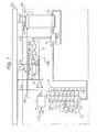
- a nonvolatile semiconductor memory device 100 is connected to a tester 200.
- a step-up circuit 11 including a charge pump circuit generates a step-up voltage V pp and transmits it to a nonvolatile cell circuit 12, particularly, its decoder portion 12a.
- the step-up voltage V pp of the step-up circuit 11 is determined by receiving a clock signal CLK via a NOR circuit 13.
- the first feedback circuit FB1 will next be explained in detail.
- the first feedback circuit FB1 is formed by a voltage divider 14, a selector 15, a reference voltage generating circuit 16 and a comparator 17.
- the voltage divider 14 is constructed by a ladder of resistors between the output of the step-up circuit 11 and the ground terminal GND.
- resistors whose resistance values are defined by R 0 , R 1 , ⁇ , R 7 is provided.
- the selector 15 is constructed by eight switches 150, 151, ..., 157. Therefore, when the switches 150, 151, ..., 157, respectively, is turned ON, the step-up voltage V pp is brought close to:
- the second feedback circuit FB2 will next be explained in detail.
- the second feedback circuit FB2 is formed by a comparator 18, a count-up signal generating circuit 19 and an up counter 20.
- the comparator 18 compares the step-up voltage V pp with the expected voltage V ppe to generate a comparison signal S 1 . Note that the comparison signal S 1 is also supplied to the tester 200.
- the count-up signal generating circuit 19 is constructed by a sampling signal generating circuit 191 for generating a sampling signal S 2 , an AND circuit 192 for passing the sampling signal in accordance with the comparison signal S 1 , and a delay circuit 193 for delaying the output signal of the AND circuit 192 to generate a count-up signal S 3 .
- the sampling signal generating circuit 191 is constructed by a counter 1911 for counting pulses of the clock signal CLK to generate a timing signal having a predetermined time period and an AND circuit 1912 for passing the timing signal in accordance with an enable signal EN from the tester 200.
- the value N of the up counter 20 is cleared by a clear signal CL from the tester 200, and is counted up by receiving the count-up signal S 3 from the count-up signal generating circuit 19.
- the value N is stored as an adjusted value N a in an adjustment area 12b of the nonvolatile cell circuit 12.
- the adjusted value N a of the adjustment area 12b of the nonvolatile cell circuit 12 is set in the counter 20 by a power-on signal PON.
- the tester 200 supplies an address signal ADD, a write signal W and the expected voltage V ppe to the nonvolatile cell circuit 12 to operate the nonvolatile cell circuit 12 even in an adjustment mode of the value N of the up counter 20.
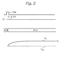
- the tester 200 generates a clear signal CL.
- the tester 200 generates an enable signal EN, so that the sampling signal generating circuit 191 is enabled.
- a sampling signal S 2 is generated from the sampling signal generating circuit 191, and subsequently, a count-up signal S 3 is generated from the count-up signal generating circuit 19.
- a sampling signal S 2 is generated from the sampling signal generating circuit 191, and subsequently, a count-up signal S 3 is generated from the count-up signal generating circuit 19.
- a sampling signal S 2 is generated from the sampling signal generating circuit 191, and subsequently, a count-up signal S 3 is generated from the count-up signal generating circuit 19.
- the tester 200 upon receipt of the change of the comparison signal S 1 , the tester 200 stops the generation of the enable signal EN, so that the sampling signal S 2 and the count-up signal S 3 are no longer generated.
- the adjustment of the value N of the up counter 20 is completed, i.e., the value N of the up counter 20 is fixed at "3".
- the tester 200 supplies a write signal W and an address signal ADD indicating the adjustment area 12b, so that the value "3" of the up counter 20 is stored in the adjustment area of the nonvolatile cell circuit 12.
- a power-on signal PON is generated from a control circuit (not shown) which also generates a read signal R and an address signal ADD indicating the adjustment area 12b.
- the value "3" is transferred from the adjustment area 12b of the nonvolatile cell circuit 12 to the up counter 20.
- the step-up voltage V pp is brought close to V 3 by the first feedback circuit.
- the value "3" of the up counter 20 is unchanged.
- a resister 18a having a relatively large resistance is connected to a terminal to which the expected value V ppe is applied.
- the expected value V ppe is 0V, the generation of count-up signals can be further suppressed, which more surely prevent a change in the value of the counter 20.
- a nonvolatile semiconductor memory device 100' is connected to a tester 200'.
- the comparator 18 of Fig. 1 is replaced by a comparator 18' whose output polarity is opposite to that of the comparator 18 of Fig. 1.
- the up counter 20 of Fig. 1 is replaced by a down counter 20', and the tester 200' generates a preset signal PS for the down counter 20' instead of the clear signal CL of Fig. 1.
- the count-up signal generating circuit 19 of Fig. 1 is replaced by a count-down signal generating circuit 19'; however, the count-down signal generating circuit 19' has the same configuration as the count-up signal generating circuit 19 of Fig. 1.
- the value N of the down counter 20' is preset by a preset signal PS from the tester 200' to a preset value such as "7", and is counted down by receiving the count-down signal S 3 ' from the count-down signal generating circuit 19'.
- the value N is stored as an adjusted value N a in the adjustment area 12b of the nonvolatile cell circuit 12.
- the adjusted value N a of the adjustment area 12b of the nonvolatile cell circuit 12 is set in the down counter 20' by a power-on signal PON.
- the tester 200' supplies an address signal ADD, a write signal W and the expected voltage V ppe to the nonvolatile cell circuit 12 to operate the nonvolatile cell circuit 12 even in an adjustment mode of the value N of the down counter 20'.
- the tester 200' generates a preset signal PS.
- the tester 200' generates an enable signal EN, so that the sampling signal generating circuit 191 is enabled.
- a sampling signal S 2 is generated from the sampling signal generating circuit 191, and subsequently, a count-down signal S 3 ' is generated from the count-down signal generating circuit 19'.
- a sampling signal S 2 is generated from the sampling signal generating circuit 191, and subsequently, a count-down signal S 3 ' is generated from the count-down signal generating circuit 19'.
- a sampling signal S 2 is generated from the sampling signal generating circuit 191, and subsequently, a count-down signal S 3 ' is generated from the count-down signal generating circuit 19'.
- the tester 200' upon receipt of the change of the comparison signal S 1 , the tester 200' stops the generation of the enable signal EN, so that the sampling signal S 2 and the count-up signal S 3 are no longer generated.
- the adjustment of the value N of the down counter 20' is completed, i.e., the value N of the down counter 20' is fixed at "4".
- the tester 200' supplies a write signal W and an address signal ADD indicating the adjustment area 12b, so that the value "4" of the down counter 20' is stored in the adjustment area of the nonvolatile cell circuit 12.
- a power-on signal PON is generated from a control circuit (not shown) which also generates a read signal R and an address signal ADD indicating the adjustment area 12b.
- the value "4" is set from the adjustment area 12b of the nonvolatile cell circuit 12 to the down counter 20'.
- the step-up voltage V pp is brought close to V 4 by the first feedback circuit.
- the value "4" of the down counter 20' is unchanged.
Landscapes
- Engineering & Computer Science (AREA)
- Power Engineering (AREA)
- Read Only Memory (AREA)
- For Increasing The Reliability Of Semiconductor Memories (AREA)
Abstract
Description
N=0
N= 1
N=2
N=3
N=7
N=6
N=5
N=4
Claims (9)
- A nonvolatile semiconductor memory device including a nonvolatile cell circuit (12) comprising:a step-up circuit (11) for receiving a clock signal (CLK) to generate a step-up voltage (Vpp) for said nonvolatile cell circuit;a voltage divider (14), connected to said step-up circuit, for dividing said step-up voltage to generate a plurality of voltages (V0, V1, ..., V7);a selector (15), connected to said voltage divider, for selecting one of said voltages;a reference voltage generating circuit (10) for generating a reference voltage (Vref);a first comparator (17), connected to said selector and said reference voltage generating circuit, for comparing said selected one of said voltages with said reference voltage;a gate circuit (13), connected to said first comparator and said step-up circuit, for supplying said clock signal to said step-up circuit in accordance with an output signal of said first comparator so that said selected one of said voltages is brought close to said reference voltage;a second comparator (18), connected to said step-up circuit, for comparing said step-up voltage with an externally-provided expected value (Vppe);a counting signal generating circuit (19, 19'), connected to said second comparator, for generating a counting signal (S3) in accordance with an output signal (S1) of said first comparator; anda counter (20, 20'), connected between said counting signal generating circuit and said selector, for changing a value (N) thereof by receiving said counting signal,said selector selecting said one of said voltages in accordance with said value of said counter, so that said step-up voltage is brought close to said expected value.
- The nonvolatile semiconductor memory device as set forth in claim 1, wherein said voltage divider comprises a ladder of resistors (R0, R1, ..., R7).
- The nonvolatile semiconductor memory device as set forth in claim 1, wherein said counter comprises an up counter (20), said counting signal being a count-up signal.
- The nonvolatile semiconductor memory device as set forth in claim 1, wherein said
counter comprises a down counter (20'), said counting signal being a count-down signal. - The nonvolatile semiconductor memory device as set forth in claim 1, wherein said counting signal generating circuit comprises:a sampling signal generating circuit (191) for generating a sampling signal (S2) having a predetermined time period; andanother gate circuit (192), connected to said sampling signal generating circuit and said second comparator, for passing said sampling signal in accordance with the output signal of said second comparator.
- The nonvolatile semiconductor memory device as set forth in claim 5, wherein said sampling signal generating circuit comprises:another counter (1911) for receiving said clock signal to generate said sampling signal; anda further gate circuit (1912), connected to said other counter, for passing said sampling signal in accordance with an externally-provided enable signal (EN).
- The nonvolatile semiconductor memory device as set forth in claim 6, further comprising a grounded resistor (191a) connected to a terminal to which said externally-provided enable signal is applied.
- The nonvolatile semiconductor memory device as set forth in claim 1, wherein said nonvolatile cell circuit comprises an adjustment area for storing the value of said counter,
the value of said counter being stored in the adjustment area of said nonvolatile cell circuit after adjustment of the value of said counter is completed,
the value in the adjustment area of said nonvolatile cell circuit being set in said counter in a post-adjustment mode. - The nonvolatile semiconductor memory device as set forth in claim 1, further comprising a grounded resistor (18a) connected to a terminal to which said externally-provided expected value is applied.
Applications Claiming Priority (2)
| Application Number | Priority Date | Filing Date | Title |
|---|---|---|---|
| JP2003008088 | 2003-01-16 | ||
| JP2003008088A JP2004220711A (en) | 2003-01-16 | 2003-01-16 | Semiconductor integrated circuit device |
Publications (2)
| Publication Number | Publication Date |
|---|---|
| EP1439545A2 true EP1439545A2 (en) | 2004-07-21 |
| EP1439545A3 EP1439545A3 (en) | 2007-03-28 |
Family
ID=32588529
Family Applications (1)
| Application Number | Title | Priority Date | Filing Date |
|---|---|---|---|
| EP04090012A Withdrawn EP1439545A3 (en) | 2003-01-16 | 2004-01-15 | Nonvolatile semiconductor memory device capable of accurately and quickly adjusting step-up voltage |
Country Status (4)
| Country | Link |
|---|---|
| US (1) | US6826085B2 (en) |
| EP (1) | EP1439545A3 (en) |
| JP (1) | JP2004220711A (en) |
| KR (1) | KR100522498B1 (en) |
Cited By (1)
| Publication number | Priority date | Publication date | Assignee | Title |
|---|---|---|---|---|
| CN114625194A (en) * | 2020-12-10 | 2022-06-14 | 圣邦微电子(北京)股份有限公司 | Reference voltage generating circuit and generating method thereof |
Families Citing this family (11)
| Publication number | Priority date | Publication date | Assignee | Title |
|---|---|---|---|---|
| KR101333503B1 (en) | 2006-02-03 | 2013-11-28 | 삼성전자주식회사 | Semiconductor memory device controlling program voltage according to number of program cells and program method thereof |
| KR100761842B1 (en) | 2006-04-07 | 2007-09-28 | 삼성전자주식회사 | Step-up circuit and step-up method for performing a step-up operation using a step-up clock signal having a variable frequency |
| KR100788573B1 (en) * | 2006-06-19 | 2007-12-26 | 주식회사 하이닉스반도체 | Reference voltage generator with self-trimming function and method of generating reference voltage |
| JP5038741B2 (en) * | 2007-02-27 | 2012-10-03 | ルネサスエレクトロニクス株式会社 | Non-volatile memory voltage generation circuit and non-volatile memory writing and erasing method |
| US7800951B2 (en) * | 2007-08-20 | 2010-09-21 | Marvell World Trade Ltd. | Threshold voltage digitizer for array of programmable threshold transistors |
| JP2009146467A (en) * | 2007-12-11 | 2009-07-02 | Toshiba Corp | Semiconductor integrated circuit device |
| JP2009146474A (en) * | 2007-12-12 | 2009-07-02 | Toshiba Corp | Nonvolatile semiconductor memory device |
| KR101522531B1 (en) * | 2008-12-30 | 2015-05-26 | 주식회사 동부하이텍 | Comparating apparatus having hysterisis characteristics, and voltage regulator using the apparatus |
| JP2011187104A (en) * | 2010-03-05 | 2011-09-22 | Renesas Electronics Corp | Nonvolatile semiconductor memory device and method of controlling the same |
| KR102469808B1 (en) * | 2016-02-12 | 2022-11-23 | 에스케이하이닉스 주식회사 | Voltage supply device of nonvolatile memory cell |
| WO2022040860A1 (en) * | 2020-08-24 | 2022-03-03 | 中国科学院微电子研究所 | Device and method for testing fatigue characteristics of gating tube |
Family Cites Families (8)
| Publication number | Priority date | Publication date | Assignee | Title |
|---|---|---|---|---|
| JP3417630B2 (en) * | 1993-12-17 | 2003-06-16 | 株式会社日立製作所 | Semiconductor integrated circuit device, flash memory and nonvolatile storage device |
| KR0185611B1 (en) * | 1995-12-11 | 1999-04-15 | 김광호 | High voltage level optimization circuit of eeprom and its method |
| FR2762435B1 (en) * | 1997-04-16 | 2000-12-08 | Sgs Thomson Microelectronics | MEMORY READING CIRCUIT WITH DYNAMICALLY CONTROLLED PRELOADING DEVICE |
| JP3145981B2 (en) | 1998-09-30 | 2001-03-12 | 日本電気アイシーマイコンシステム株式会社 | Semiconductor nonvolatile storage device |
| JP3854025B2 (en) * | 1998-12-25 | 2006-12-06 | 株式会社東芝 | Nonvolatile semiconductor memory device |
| US6304487B1 (en) * | 2000-02-28 | 2001-10-16 | Advanced Micro Devices, Inc. | Register driven means to control programming voltages |
| IT1318892B1 (en) * | 2000-09-15 | 2003-09-19 | St Microelectronics Srl | SEMICONDUCTOR READING CIRCUIT FOR NON-VOLATILE MEMORIES. |
| JP4790158B2 (en) * | 2001-06-11 | 2011-10-12 | ルネサスエレクトロニクス株式会社 | Semiconductor device |
-
2003
- 2003-01-16 JP JP2003008088A patent/JP2004220711A/en active Pending
-
2004
- 2004-01-05 KR KR10-2004-0000238A patent/KR100522498B1/en not_active Expired - Fee Related
- 2004-01-05 US US10/750,970 patent/US6826085B2/en not_active Expired - Fee Related
- 2004-01-15 EP EP04090012A patent/EP1439545A3/en not_active Withdrawn
Cited By (1)
| Publication number | Priority date | Publication date | Assignee | Title |
|---|---|---|---|---|
| CN114625194A (en) * | 2020-12-10 | 2022-06-14 | 圣邦微电子(北京)股份有限公司 | Reference voltage generating circuit and generating method thereof |
Also Published As
| Publication number | Publication date |
|---|---|
| US6826085B2 (en) | 2004-11-30 |
| US20040141376A1 (en) | 2004-07-22 |
| EP1439545A3 (en) | 2007-03-28 |
| KR100522498B1 (en) | 2005-10-18 |
| JP2004220711A (en) | 2004-08-05 |
| KR20040065999A (en) | 2004-07-23 |
Similar Documents
| Publication | Publication Date | Title |
|---|---|---|
| US7002869B2 (en) | Voltage regulator circuit | |
| US7551507B2 (en) | Power supply circuit and semiconductor memory | |
| JP6886545B1 (en) | Power-down detection circuit and semiconductor storage device | |
| US9413338B2 (en) | Apparatuses, methods, and circuits including a duty cycle adjustment circuit | |
| EP1439545A2 (en) | Nonvolatile semiconductor memory device capable of accurately and quickly adjusting step-up voltage | |
| US8008978B2 (en) | Oscillator circuit and memory system | |
| US7439794B2 (en) | Power source circuit | |
| US7697342B2 (en) | Flash memory device and related high voltage generating circuit | |
| US8693268B2 (en) | Semiconductor device | |
| EP1324347B1 (en) | A circuit for controlling a reference node in a sense amplifier | |
| US8098528B2 (en) | Voltage generation circuit and nonvolatile memory device including the same | |
| US9019003B2 (en) | Voltage generation circuit | |
| US7881129B2 (en) | High voltage regulator for non-volatile memory device | |
| US6040994A (en) | Method for writing in an electrically modifiable non-volatile memory | |
| US7596029B2 (en) | Flash memory device including unified oscillation circuit and method of operating the device | |
| CN110299173B (en) | Controllable discharging module for NOR FLASH programming processing | |
| US9105356B2 (en) | Semiconductor device | |
| JP2007005776A (en) | Semiconductor device | |
| US10658052B2 (en) | Semiconductor device | |
| JP5520524B2 (en) | Power supply circuit for memory writing | |
| KR101088468B1 (en) | Voltage generation circuit and nonvolatile memory device having same | |
| KR20150034833A (en) | Circuit and method for programming voltage level and delay time |
Legal Events
| Date | Code | Title | Description |
|---|---|---|---|
| PUAI | Public reference made under article 153(3) epc to a published international application that has entered the european phase |
Free format text: ORIGINAL CODE: 0009012 |
|
| AK | Designated contracting states |
Kind code of ref document: A2 Designated state(s): AT BE BG CH CY CZ DE DK EE ES FI FR GB GR HU IE IT LI LU MC NL PT RO SE SI SK TR |
|
| AX | Request for extension of the european patent |
Extension state: AL LT LV MK |
|
| PUAL | Search report despatched |
Free format text: ORIGINAL CODE: 0009013 |
|
| AK | Designated contracting states |
Kind code of ref document: A3 Designated state(s): AT BE BG CH CY CZ DE DK EE ES FI FR GB GR HU IE IT LI LU MC NL PT RO SE SI SK TR |
|
| AX | Request for extension of the european patent |
Extension state: AL LT LV MK |
|
| STAA | Information on the status of an ep patent application or granted ep patent |
Free format text: STATUS: THE APPLICATION HAS BEEN WITHDRAWN |
|
| 17P | Request for examination filed |
Effective date: 20070414 |
|
| 18W | Application withdrawn |
Effective date: 20070511 |