EP1437746A2 - Nanomagnetic materials - Google Patents
Nanomagnetic materials Download PDFInfo
- Publication number
- EP1437746A2 EP1437746A2 EP04006047A EP04006047A EP1437746A2 EP 1437746 A2 EP1437746 A2 EP 1437746A2 EP 04006047 A EP04006047 A EP 04006047A EP 04006047 A EP04006047 A EP 04006047A EP 1437746 A2 EP1437746 A2 EP 1437746A2
- Authority
- EP
- European Patent Office
- Prior art keywords
- nanomagnets
- anisotropy
- magnetic
- field
- nanomagnet
- Prior art date
- Legal status (The legal status is an assumption and is not a legal conclusion. Google has not performed a legal analysis and makes no representation as to the accuracy of the status listed.)
- Granted
Links
- 239000000463 material Substances 0.000 title description 11
- 239000000696 magnetic material Substances 0.000 claims description 17
- 229910000815 supermalloy Inorganic materials 0.000 claims description 5
- 239000000758 substrate Substances 0.000 claims description 4
- 230000006870 function Effects 0.000 description 6
- 238000000034 method Methods 0.000 description 6
- 229910045601 alloy Inorganic materials 0.000 description 4
- 239000000956 alloy Substances 0.000 description 4
- 230000006399 behavior Effects 0.000 description 4
- 230000000694 effects Effects 0.000 description 4
- 238000005259 measurement Methods 0.000 description 4
- 239000002086 nanomaterial Substances 0.000 description 4
- 239000012237 artificial material Substances 0.000 description 3
- 230000008859 change Effects 0.000 description 3
- 230000003247 decreasing effect Effects 0.000 description 3
- 238000002050 diffraction method Methods 0.000 description 3
- 239000000523 sample Substances 0.000 description 3
- 238000007725 thermal activation Methods 0.000 description 3
- XUIMIQQOPSSXEZ-UHFFFAOYSA-N Silicon Chemical compound [Si] XUIMIQQOPSSXEZ-UHFFFAOYSA-N 0.000 description 2
- 230000004888 barrier function Effects 0.000 description 2
- 239000000470 constituent Substances 0.000 description 2
- 238000013500 data storage Methods 0.000 description 2
- 238000000609 electron-beam lithography Methods 0.000 description 2
- 239000006249 magnetic particle Substances 0.000 description 2
- 230000003287 optical effect Effects 0.000 description 2
- 230000010355 oscillation Effects 0.000 description 2
- 230000008569 process Effects 0.000 description 2
- 230000035945 sensitivity Effects 0.000 description 2
- 229910052710 silicon Inorganic materials 0.000 description 2
- 239000010703 silicon Substances 0.000 description 2
- 230000005374 Kerr effect Effects 0.000 description 1
- 238000004458 analytical method Methods 0.000 description 1
- 239000013590 bulk material Substances 0.000 description 1
- 239000002178 crystalline material Substances 0.000 description 1
- 238000002474 experimental method Methods 0.000 description 1
- PCHJSUWPFVWCPO-UHFFFAOYSA-N gold Chemical compound [Au] PCHJSUWPFVWCPO-UHFFFAOYSA-N 0.000 description 1
- 239000010931 gold Substances 0.000 description 1
- 229910052737 gold Inorganic materials 0.000 description 1
- 229910001004 magnetic alloy Inorganic materials 0.000 description 1
- 230000006386 memory function Effects 0.000 description 1
- 229910021421 monocrystalline silicon Inorganic materials 0.000 description 1
- 230000003647 oxidation Effects 0.000 description 1
- 238000007254 oxidation reaction Methods 0.000 description 1
- 229910000889 permalloy Inorganic materials 0.000 description 1
- 230000035699 permeability Effects 0.000 description 1
- 230000005610 quantum mechanics Effects 0.000 description 1
- 239000013079 quasicrystal Substances 0.000 description 1
- 238000011160 research Methods 0.000 description 1
- 230000000630 rising effect Effects 0.000 description 1
- 238000001878 scanning electron micrograph Methods 0.000 description 1
- 238000004626 scanning electron microscopy Methods 0.000 description 1
- 239000004065 semiconductor Substances 0.000 description 1
- 238000007493 shaping process Methods 0.000 description 1
- 125000006850 spacer group Chemical group 0.000 description 1
- 230000003068 static effect Effects 0.000 description 1
- 230000003746 surface roughness Effects 0.000 description 1
- 238000012360 testing method Methods 0.000 description 1
Images




Classifications
-
- B—PERFORMING OPERATIONS; TRANSPORTING
- B82—NANOTECHNOLOGY
- B82Y—SPECIFIC USES OR APPLICATIONS OF NANOSTRUCTURES; MEASUREMENT OR ANALYSIS OF NANOSTRUCTURES; MANUFACTURE OR TREATMENT OF NANOSTRUCTURES
- B82Y25/00—Nanomagnetism, e.g. magnetoimpedance, anisotropic magnetoresistance, giant magnetoresistance or tunneling magnetoresistance
-
- G—PHYSICS
- G11—INFORMATION STORAGE
- G11C—STATIC STORES
- G11C11/00—Digital stores characterised by the use of particular electric or magnetic storage elements; Storage elements therefor
- G11C11/02—Digital stores characterised by the use of particular electric or magnetic storage elements; Storage elements therefor using magnetic elements
-
- B—PERFORMING OPERATIONS; TRANSPORTING
- B82—NANOTECHNOLOGY
- B82Y—SPECIFIC USES OR APPLICATIONS OF NANOSTRUCTURES; MEASUREMENT OR ANALYSIS OF NANOSTRUCTURES; MANUFACTURE OR TREATMENT OF NANOSTRUCTURES
- B82Y10/00—Nanotechnology for information processing, storage or transmission, e.g. quantum computing or single electron logic
-
- G—PHYSICS
- G01—MEASURING; TESTING
- G01R—MEASURING ELECTRIC VARIABLES; MEASURING MAGNETIC VARIABLES
- G01R33/00—Arrangements or instruments for measuring magnetic variables
- G01R33/02—Measuring direction or magnitude of magnetic fields or magnetic flux
-
- G—PHYSICS
- G11—INFORMATION STORAGE
- G11B—INFORMATION STORAGE BASED ON RELATIVE MOVEMENT BETWEEN RECORD CARRIER AND TRANSDUCER
- G11B5/00—Recording by magnetisation or demagnetisation of a record carrier; Reproducing by magnetic means; Record carriers therefor
- G11B5/62—Record carriers characterised by the selection of the material
- G11B5/64—Record carriers characterised by the selection of the material comprising only the magnetic material without bonding agent
- G11B5/65—Record carriers characterised by the selection of the material comprising only the magnetic material without bonding agent characterised by its composition
- G11B5/653—Record carriers characterised by the selection of the material comprising only the magnetic material without bonding agent characterised by its composition containing Fe or Ni
-
- G—PHYSICS
- G11—INFORMATION STORAGE
- G11B—INFORMATION STORAGE BASED ON RELATIVE MOVEMENT BETWEEN RECORD CARRIER AND TRANSDUCER
- G11B5/00—Recording by magnetisation or demagnetisation of a record carrier; Reproducing by magnetic means; Record carriers therefor
- G11B5/74—Record carriers characterised by the form, e.g. sheet shaped to wrap around a drum
- G11B5/743—Patterned record carriers, wherein the magnetic recording layer is patterned into magnetic isolated data islands, e.g. discrete tracks
- G11B5/746—Bit Patterned record carriers, wherein each magnetic isolated data island corresponds to a bit
-
- G—PHYSICS
- G11—INFORMATION STORAGE
- G11C—STATIC STORES
- G11C11/00—Digital stores characterised by the use of particular electric or magnetic storage elements; Storage elements therefor
- G11C11/02—Digital stores characterised by the use of particular electric or magnetic storage elements; Storage elements therefor using magnetic elements
- G11C11/16—Digital stores characterised by the use of particular electric or magnetic storage elements; Storage elements therefor using magnetic elements using elements in which the storage effect is based on magnetic spin effect
- G11C11/161—Digital stores characterised by the use of particular electric or magnetic storage elements; Storage elements therefor using magnetic elements using elements in which the storage effect is based on magnetic spin effect details concerning the memory cell structure, e.g. the layers of the ferromagnetic memory cell
-
- H—ELECTRICITY
- H01—ELECTRIC ELEMENTS
- H01F—MAGNETS; INDUCTANCES; TRANSFORMERS; SELECTION OF MATERIALS FOR THEIR MAGNETIC PROPERTIES
- H01F1/00—Magnets or magnetic bodies characterised by the magnetic materials therefor; Selection of materials for their magnetic properties
- H01F1/0018—Diamagnetic or paramagnetic materials, i.e. materials with low susceptibility and no hysteresis
-
- H—ELECTRICITY
- H01—ELECTRIC ELEMENTS
- H01F—MAGNETS; INDUCTANCES; TRANSFORMERS; SELECTION OF MATERIALS FOR THEIR MAGNETIC PROPERTIES
- H01F1/00—Magnets or magnetic bodies characterised by the magnetic materials therefor; Selection of materials for their magnetic properties
- H01F1/0036—Magnets or magnetic bodies characterised by the magnetic materials therefor; Selection of materials for their magnetic properties showing low dimensional magnetism, i.e. spin rearrangements due to a restriction of dimensions, e.g. showing giant magnetoresistivity
- H01F1/009—Magnets or magnetic bodies characterised by the magnetic materials therefor; Selection of materials for their magnetic properties showing low dimensional magnetism, i.e. spin rearrangements due to a restriction of dimensions, e.g. showing giant magnetoresistivity bidimensional, e.g. nanoscale period nanomagnet arrays
-
- H—ELECTRICITY
- H03—ELECTRONIC CIRCUITRY
- H03K—PULSE TECHNIQUE
- H03K19/00—Logic circuits, i.e. having at least two inputs acting on one output; Inverting circuits
- H03K19/02—Logic circuits, i.e. having at least two inputs acting on one output; Inverting circuits using specified components
- H03K19/16—Logic circuits, i.e. having at least two inputs acting on one output; Inverting circuits using specified components using saturable magnetic devices
- H03K19/168—Logic circuits, i.e. having at least two inputs acting on one output; Inverting circuits using specified components using saturable magnetic devices using thin-film devices
-
- G—PHYSICS
- G11—INFORMATION STORAGE
- G11B—INFORMATION STORAGE BASED ON RELATIVE MOVEMENT BETWEEN RECORD CARRIER AND TRANSDUCER
- G11B5/00—Recording by magnetisation or demagnetisation of a record carrier; Reproducing by magnetic means; Record carriers therefor
- G11B5/74—Record carriers characterised by the form, e.g. sheet shaped to wrap around a drum
-
- G—PHYSICS
- G11—INFORMATION STORAGE
- G11B—INFORMATION STORAGE BASED ON RELATIVE MOVEMENT BETWEEN RECORD CARRIER AND TRANSDUCER
- G11B5/00—Recording by magnetisation or demagnetisation of a record carrier; Reproducing by magnetic means; Record carriers therefor
- G11B5/74—Record carriers characterised by the form, e.g. sheet shaped to wrap around a drum
- G11B5/82—Disk carriers
-
- Y—GENERAL TAGGING OF NEW TECHNOLOGICAL DEVELOPMENTS; GENERAL TAGGING OF CROSS-SECTIONAL TECHNOLOGIES SPANNING OVER SEVERAL SECTIONS OF THE IPC; TECHNICAL SUBJECTS COVERED BY FORMER USPC CROSS-REFERENCE ART COLLECTIONS [XRACs] AND DIGESTS
- Y10—TECHNICAL SUBJECTS COVERED BY FORMER USPC
- Y10S—TECHNICAL SUBJECTS COVERED BY FORMER USPC CROSS-REFERENCE ART COLLECTIONS [XRACs] AND DIGESTS
- Y10S428/00—Stock material or miscellaneous articles
- Y10S428/90—Magnetic feature
-
- Y—GENERAL TAGGING OF NEW TECHNOLOGICAL DEVELOPMENTS; GENERAL TAGGING OF CROSS-SECTIONAL TECHNOLOGIES SPANNING OVER SEVERAL SECTIONS OF THE IPC; TECHNICAL SUBJECTS COVERED BY FORMER USPC CROSS-REFERENCE ART COLLECTIONS [XRACs] AND DIGESTS
- Y10—TECHNICAL SUBJECTS COVERED BY FORMER USPC
- Y10T—TECHNICAL SUBJECTS COVERED BY FORMER US CLASSIFICATION
- Y10T428/00—Stock material or miscellaneous articles
- Y10T428/12—All metal or with adjacent metals
- Y10T428/12465—All metal or with adjacent metals having magnetic properties, or preformed fiber orientation coordinate with shape
-
- Y—GENERAL TAGGING OF NEW TECHNOLOGICAL DEVELOPMENTS; GENERAL TAGGING OF CROSS-SECTIONAL TECHNOLOGIES SPANNING OVER SEVERAL SECTIONS OF THE IPC; TECHNICAL SUBJECTS COVERED BY FORMER USPC CROSS-REFERENCE ART COLLECTIONS [XRACs] AND DIGESTS
- Y10—TECHNICAL SUBJECTS COVERED BY FORMER USPC
- Y10T—TECHNICAL SUBJECTS COVERED BY FORMER US CLASSIFICATION
- Y10T428/00—Stock material or miscellaneous articles
- Y10T428/12—All metal or with adjacent metals
- Y10T428/12493—Composite; i.e., plural, adjacent, spatially distinct metal components [e.g., layers, joint, etc.]
- Y10T428/12771—Transition metal-base component
- Y10T428/12861—Group VIII or IB metal-base component
- Y10T428/12951—Fe-base component
Definitions
- This invention relates to magnetic materials and, in particular, to the use of rotational symmetry to tailor the magnetic properties of the materials.
- nanomagnets The volume of information which can be stored on a computer hard disk has risen by a factor of 10 7 in the past 40 years and looks set to continue rising at an exponential rate in coming decades.
- Each nanomagnet is analogous to a giant atom of an artificial element, allowing new magnetic materials to be built up giant atom by giant atom.
- the rapidly growing field of nanomagnetism may provide among other things advanced replacements for hard disk media and a new generation of high speed, low power, non-volatile computer memory chips.
- the most important property of a naturally occurring magnetic element or alloy is its anisotropy. This refers to the presence of preferred magnetisation directions within the material and is ultimately responsible for determining the way in which a magnetic material behaves and the technological applications for which it is suitable.
- anisotropy arises from the shape and symmetry of the electronic Fermi surface and so is intrinsic to the particular element or alloy and cannot easily be tailored.
- nanomagnets however, the anisotropy depends not only on the band structure of the parent material, but also on the shape of the nanomagnet.
- One of the most attractive features of artificial magnetic materials is that their magnetic properties can be engineered by the choice of the shape of the constituent nanomagnets.
- a sensor element comprises nanomagnets having a rotational symmetry selected such that they are superparamagnetic and exhibit substantially zero hysteresis so that a magnetisation of the nanomagnets depends only on the current value of applied field and not on the field history.
- a magnetic logic element comprises nanomagnets having a rotational symmetry selected such that they are superparamagnetic and exhibit substantially zero hysteresis so that a magnetisation of the nanomagnets depends only on the current value of applied field and not on the field history.
- the devices of the invention are artificial magnetic materials formed on the surface of a substrate, such as a piece of silicon, using a technique such as electron beam lithography.
- the devices may be in the size range 40-500nm and in the thickness range 3-10nm and may be, triangular, or pentagonal-geometries which respectively correspond to rotational symmetries of order 3 and 5. The order may, however, be greater.
- the parent material may be Supermalloy (Ni 80 Fe 14 Mo 5 ), which is chosen for two reasons. Firstly, this alloy is intrinsically almost isotropic and so any anisotropy in the nanomagnets must come from their shape.
- Supermalloy and its molybdenum-free relative Permalloy are two of the ubiquitous soft magnetic alloys of industry and research and as such make an effective demonstration of the new and varied properties which can be given to a simple material by nanometric structuring. As described below, we are able to make artificial magnetic materials with an enormously wide range of magnetic properties simply by varying the symmetry of the constituent nanomagnets.
- a standard lift-off based electron beam lithography process can be employed to form devices according to the present invention.
- the sample substrate was oriented single crystal silicon.
- the spacing between each nanomagnet was always at least equal to the diameter of the nanomagnet, and for the smallest structures was as large as 3 times the diameter.
- the surface roughness of the nanomagnets was less than 0.5nm and the microstructure showed 5nm randomly oriented grains.
- the top surface of each nanomagnet was covered with a 5nm thick layer of gold to prevent oxidation.
- the integrity of the geometric shape was found to be preserved in structures as small as 50nm in size.
- Figure 1 shows Scanning Electron Microscopy images of some of the structures.
- M-H loops hysteresis loops
- the silicon surface can be viewed under an optical microscope while a laser spot (size ⁇ 5 ⁇ m) is moved over the surface until focused on top of one of the patches of artificial material.
- the reflected laser beam is polarisation analysed in order to access the longitudinal Kerr effect, which serves as a probe of the component of magnetisation lying in the optical plane of incidence. This magnetisation is then recorded while a 27Hz alternating magnetic field of up to 1000 Oe strength is applied in the plane of the sample. All measurements were performed at room temperature.
- Figures 2 and 3 show some of the hysteresis loops measured from nanomagnets of different size, thickness and geometric shape. One sees immediately that the loops are very different from each other and from that obtained from the conventional unstructured material. The variety of technological applications covered by the samples represented in this figure is considerable.
- the known small rectangles shown in Figure 2B could be suitable for making an artificial replacement for hard disk media: the nanomagnets used here could in principle achieve data storage densities in excess of 100 Gbits/inch 2 , i.e. 10 times greater than today's state-of-the-art conventional media.
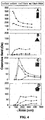
- Coercivity is a measure of the applied field necessary to reduce the magnetisation to zero (i.e. hysteresis loops have a central width of twice the Coercivity) and as such is a measure of how readily an external field can reverse the magnetisation direction of a nanomagnet. This is a key parameter in assessing the suitability of a given magnetic material for technological applications.
- Figure 4 shows the results, where, in order to be able to compare different geometries, we express the size of the nanomagnets by the square root of their area. We have confirmed the repeatability of certain of these experimental results on a second set of samples.
- the first apparent feature from the data of Figure 4 is that the 2-fold and 4-fold symmetries display one class of behaviour while the 3-fold and 5-fold symmetries display another class: 2- /4- fold nanomagnets show high coercivities which at first rise with decreasing lengthscale; 3- /5- fold nanomagnets show low coercivities which fall to zero with decreasing lengthscale.
- 2- /4- fold nanomagnets show high coercivities which at first rise with decreasing lengthscale
- 3- /5- fold nanomagnets show low coercivities which fall to zero with decreasing lengthscale.
- the second observation which can be made about Figure 4 is that in all cases increasing the thickness leads to a strong rise in coercivity, which is not the case in unstructured magnetic films.
- the behaviour of the 2-fold nanomagnets is very straightforward and is due to a well understood phenomenon called shape anisotropy.
- the magnetisation prefers to "streamline" with the longest axis of the nanomagnet in order to minimise the surface area of the pole faces.
- the field driving this effect is the demagnetising field which passes between pole faces through the inside of the magnet.
- the demagnetising field scales approximately with the ratio t/a where t is the thickness of the nanomagnet and a is its size and so one sees in Figure 4A a coercivity which rises with decreasing size.
- the amplitude of the resulting oscillation of the magnetisation is recorded by the same magnetooptical technique used to obtain the hysteresis loops of Figures 2 and 3 and is directly related to the amplitude and symmetry of any anisotropy present in the nanomagnet.
- H a 1 M s ⁇ 2 E ⁇ 2 for a nanomagnet of that size
- M s the saturation magnetisation (800 emu cm -3 )
- E( ⁇ ) the average magnetic energy density of the nanomagnet when magnetised in the direction ⁇ .
- H a is not the usual definition of anisotropy field, it can be shown that any oscillations in H a have the same symmetry order as the underlying anisotropy and an amplitude equal to the magnitude of the anisotropy field.
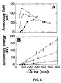
- Figure 5 shows experimental data from 22 different samples of artificial magnetic material (8 sizes of triangles, 8 sizes of squares and 6 sizes of pentagons), each measured in either 19 or 37 different directions ⁇ (0-180° in 10° steps for triangles and squares, 0-180° in 5° steps for pentagons) making a total of 526 measurements.
- U a is the anisotropy energy of a single nanomagnet (in ergs)
- H a is the anisotropy field (in Oe)
- n is the symmetry order of the anisotropy (4 for squares, 6 for triangles, 10 for pentagons)
- V is the volume (in cm 3 ) of the nanomagnet.
- the anisotropy energy is particularly interesting because of a phenomenon called superparamagnetism, which is the process by which anisotropy energy barriers can be overcome by the kT thermal energy fluctuations in nanometre scale magnets.
- superparamagnetism is the process by which anisotropy energy barriers can be overcome by the kT thermal energy fluctuations in nanometre scale magnets.
- a barrier can be overcome on the timescale of our measurements once it is less than 10kT in height. This means that once the anisotropy energy is less than 10kT, one would expect the coercivity to fall rapidly to zero. According to Figure 6B this should occur once the element size is less than approximately 150nm, the squares being last to fall as the size is reduced. Conversely, once the anisotropy energy is greater than 10kT, the coercivity should approximately follow the anisotropy field.
- High remanence materials possessing finite coercivity are not the only technologically important magnetic materials. Equally important are the zero remanence, zero coercivity materials which find applications in magnetic sensors and logic elements and in this case it is the susceptibility, ⁇ , which is the key parameter. ⁇ is defined as 4 ⁇ M / ⁇ H where M is the magnetisation of a nanomagnet and H is the applied magnetic field. ⁇ is thus directly proportional to the zero field slope of hysteres is loops such as that shown in Figure 2F.
- the deviations from the Langevin model are greatest for the square symmetry nanomagnets. This is consistent with these possessing the strongest configurational anisotropy energy, meaning that the giant spin contained in a square nanomagnet looks least like a giant spin in free space. It is configurational anisotropy which eventually causes all of the symmetries to fall away from the Langevin model with increasing size.
- the susceptibilities measured here are two orders of magnitude greater than would have been obtained from magnetic particles of the same shape and aspect ratio but made on a larger than nanometre lengthscale (i.e. micrometers and above, as most conventional magnetic field sensors use). In this latter case, susceptibility comes from the motion of domain walls against the internal demagnetising field, which can be very strong. The unique role of nanometre scale structuring is thus clearly demonstrated.
- Figure 4 and Figure 5 illustrate well the way in which nanometric structuring really does emulate the creation of new magnetic materials.
- Supermalloy grows with f.c.c. crystallography which usually results in 2- or 4-fold anisotropy.
- Figure 5A exhibits 6-fold symmetry which is usually reserved for materials with h.c.p. crystallography.
- the symmetry of the nanomagnet shape (triangular) can be used to emulate a change in crystallographic phase.
- the relatively high coercivities of square and rectangular nanomagnets would usually only be found in magnetic materials with a high anisotropy and a weakly coupled microstructure.
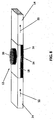
- FIG. 8 shows a possible arrangement using a superparamagnetic nanomagnet as part of a sensor or logic element.
- a trilayer spin valve 12 is joined at both sides to connector lines 14.
- the valve 12 comprises a magnetic bottom layer 16, a non-magnetic spacer layer 18 and one or more nanomagnets 20 in a superparamagnetic state as a top layer.
- Arrows 22 indicate the passage of current across the valve 12 and arrow 24 indicates the magnetisation in the magnetic bottom layer 16.
- the first new idea is the use of configurational anisotropy via the symmetry of the element to tailor magnetic properties.
- people in the art have only considered rectangular, square or circular elements.
- the configurational anisotropy induced by other shapes such as triangles, pentagons and hexagons can be used to control the magnetic properties of the element.
- the second new idea is the use of superparamagnetism in nanostructures to remove hysteresis.
- superaparamagnetism leads to very high saturation fields, and as such is no use for magnetic sensors.
Landscapes
- Engineering & Computer Science (AREA)
- Chemical & Material Sciences (AREA)
- Nanotechnology (AREA)
- Physics & Mathematics (AREA)
- Crystallography & Structural Chemistry (AREA)
- Mathematical Physics (AREA)
- Computer Hardware Design (AREA)
- Condensed Matter Physics & Semiconductors (AREA)
- Power Engineering (AREA)
- Theoretical Computer Science (AREA)
- General Physics & Mathematics (AREA)
- General Engineering & Computer Science (AREA)
- Computing Systems (AREA)
- Hard Magnetic Materials (AREA)
- Hall/Mr Elements (AREA)
- Thin Magnetic Films (AREA)
- Soft Magnetic Materials (AREA)
- Measuring Magnetic Variables (AREA)
- Valve Device For Special Equipments (AREA)
- Magnetic Record Carriers (AREA)
- Transmission And Conversion Of Sensor Element Output (AREA)
- Electrochromic Elements, Electrophoresis, Or Variable Reflection Or Absorption Elements (AREA)
Abstract
Description
Claims (10)
- A sensor element comprising nanomagnets having a geometric rotational symmetry around an axis selected such that they are superparamagnetic and exhibit substantially zero hysteresis so that a magnetisation of the nanomagnets depends only on the current value of applied field and not on the field history.
- A sensor element according to claim 1, formed from an artificial magnetic material formed on the surface of a substrate the axis being substantially perpendicular to the surface.
- A sensor element according to claim 1 or 2, formed from Supermalloy (Ni80Fe14Mo5).
- A sensor element according to any of claims 1, 2 or 3 the size range 40-500nm per side and in the thickness range 3-10nm.
- A sensor element according to any of claims 1 to 4, having rotational symmetries to the order 3 or 5.
- A magnetic logic element comprising nanomagnets having a geometric rotational symmetry around an axis selected such that they are superparamagnetic and exhibit substantially zero hysteresis so that a magnetisation of the nanomagnets depends only on the current value of applied field and not on the field history.
- A logic element according to claim 6, formed from an artificial magnetic material formed on the surface of a substrate, the axis being substantially perpendicular to the surface.
- A logic element according to claim 6 or 7, formed from Supermalloy (Ni80Fe14Mo5).
- A logic element according to any of claims 6, 7 or 8 the size range 40-500nm per side and in the thickness range 3-10nm.
- A logic element according to any of claims 6 to 9, having rotational symmetries to the order 3 or 5.
Priority Applications (1)
| Application Number | Priority Date | Filing Date | Title |
|---|---|---|---|
| EP05016528A EP1598834B1 (en) | 1999-04-09 | 2000-04-07 | Magnetic logic element |
Applications Claiming Priority (3)
| Application Number | Priority Date | Filing Date | Title |
|---|---|---|---|
| GBGB9908179.6A GB9908179D0 (en) | 1999-04-09 | 1999-04-09 | Magnetic materials |
| GB9908179 | 1999-04-09 | ||
| EP00919026A EP1169720B1 (en) | 1999-04-09 | 2000-04-07 | Magnetic materials |
Related Parent Applications (1)
| Application Number | Title | Priority Date | Filing Date |
|---|---|---|---|
| EP00919026A Division EP1169720B1 (en) | 1999-04-09 | 2000-04-07 | Magnetic materials |
Related Child Applications (1)
| Application Number | Title | Priority Date | Filing Date |
|---|---|---|---|
| EP05016528A Division EP1598834B1 (en) | 1999-04-09 | 2000-04-07 | Magnetic logic element |
Publications (3)
| Publication Number | Publication Date |
|---|---|
| EP1437746A2 true EP1437746A2 (en) | 2004-07-14 |
| EP1437746A3 EP1437746A3 (en) | 2004-09-08 |
| EP1437746B1 EP1437746B1 (en) | 2006-10-04 |
Family
ID=10851267
Family Applications (3)
| Application Number | Title | Priority Date | Filing Date |
|---|---|---|---|
| EP05016528A Expired - Lifetime EP1598834B1 (en) | 1999-04-09 | 2000-04-07 | Magnetic logic element |
| EP04006047A Expired - Lifetime EP1437746B1 (en) | 1999-04-09 | 2000-04-07 | Nanomagnetic materials |
| EP00919026A Expired - Lifetime EP1169720B1 (en) | 1999-04-09 | 2000-04-07 | Magnetic materials |
Family Applications Before (1)
| Application Number | Title | Priority Date | Filing Date |
|---|---|---|---|
| EP05016528A Expired - Lifetime EP1598834B1 (en) | 1999-04-09 | 2000-04-07 | Magnetic logic element |
Family Applications After (1)
| Application Number | Title | Priority Date | Filing Date |
|---|---|---|---|
| EP00919026A Expired - Lifetime EP1169720B1 (en) | 1999-04-09 | 2000-04-07 | Magnetic materials |
Country Status (15)
| Country | Link |
|---|---|
| US (1) | US6614084B1 (en) |
| EP (3) | EP1598834B1 (en) |
| JP (3) | JP4287062B2 (en) |
| KR (1) | KR100699611B1 (en) |
| CN (1) | CN1251251C (en) |
| AT (3) | ATE341821T1 (en) |
| AU (1) | AU763157B2 (en) |
| CA (1) | CA2366588A1 (en) |
| DE (3) | DE60031181T2 (en) |
| DK (1) | DK1169720T3 (en) |
| ES (1) | ES2225119T3 (en) |
| GB (1) | GB9908179D0 (en) |
| PT (1) | PT1169720E (en) |
| RU (3) | RU2244971C2 (en) |
| WO (1) | WO2000062311A1 (en) |
Families Citing this family (13)
| Publication number | Priority date | Publication date | Assignee | Title |
|---|---|---|---|---|
| GB9925213D0 (en) | 1999-10-25 | 1999-12-22 | Univ Cambridge Tech | Magnetic logic elements |
| US7733350B2 (en) * | 2006-06-30 | 2010-06-08 | Microsoft Corporation | Anisometric texture synthesis |
| US8134441B1 (en) * | 2008-06-02 | 2012-03-13 | The Regents Of The University Of California | Nanomagnetic signal propagation and logic gates |
| US8138874B1 (en) | 2009-07-20 | 2012-03-20 | The Regents Of The University Of California | Nanomagnetic register |
| WO2011044100A2 (en) * | 2009-10-05 | 2011-04-14 | University Of Delaware | Ferromagnetic resonance and memory effect in magnetic composite materials |
| US9196280B2 (en) * | 2009-11-12 | 2015-11-24 | Marquette University | Low-field magnetic domain wall injection pad and high-density storage wire |
| KR200452028Y1 (en) * | 2010-02-23 | 2011-02-01 | 정진시그널(주) | Road sign with transparent reflector |
| US8766754B2 (en) | 2012-07-18 | 2014-07-01 | The Regents Of The University Of California | Concave nanomagnets with widely tunable anisotropy |
| US9460737B2 (en) | 2013-04-18 | 2016-10-04 | Headway Technologies, Inc. | Supermalloy and mu metal side and top shields for magnetic read heads |
| FR3031622B1 (en) * | 2015-01-14 | 2018-02-16 | Centre National De La Recherche Scientifique | MAGNETIC MEMORY POINT |
| JP6821665B2 (en) * | 2015-06-04 | 2021-01-27 | エンドマグネティクス リミテッド | Magnetic marker |
| JP7565563B2 (en) * | 2021-05-14 | 2024-10-11 | 国立大学法人東北大学 | Magnetic metamaterial, spin current control device and spin current control method |
| CN119626285B (en) * | 2024-11-06 | 2025-07-18 | 云南大学 | Magnetic nano multi-ring memory device and preparation method and application thereof |
Family Cites Families (17)
| Publication number | Priority date | Publication date | Assignee | Title |
|---|---|---|---|---|
| US3873914A (en) * | 1973-07-18 | 1975-03-25 | Sperry Rand Corp | Flux valve apparatus for sensing both horizontal and vertical components of an ambient magnetic field |
| RU2006965C1 (en) * | 1990-08-09 | 1994-01-30 | Московский институт электронной техники | Read-only storage item |
| JPH0810653B2 (en) * | 1990-11-22 | 1996-01-31 | 科学技術庁金属材料技術研究所長 | Array lattice structure of magnetic particles |
| RU2029391C1 (en) * | 1991-06-28 | 1995-02-20 | Тимошков Юрий Викторович | Storage element |
| US5710436A (en) | 1994-09-27 | 1998-01-20 | Kabushiki Kaisha Toshiba | Quantum effect device |
| US5654566A (en) * | 1995-04-21 | 1997-08-05 | Johnson; Mark B. | Magnetic spin injected field effect transistor and method of operation |
| RU2093905C1 (en) * | 1995-05-23 | 1997-10-20 | Институт проблем управления РАН | Gate with memory |
| US5741435A (en) * | 1995-08-08 | 1998-04-21 | Nano Systems, Inc. | Magnetic memory having shape anisotropic magnetic elements |
| US5714536A (en) * | 1996-01-11 | 1998-02-03 | Xerox Corporation | Magnetic nanocompass compositions and processes for making and using |
| JPH09298320A (en) * | 1996-05-09 | 1997-11-18 | Kobe Steel Ltd | Persistent current switch for oxide superconducting coil, switch device using the same, and switching method |
| RU2120142C1 (en) * | 1996-07-02 | 1998-10-10 | Институт проблем управления РАН | Magnetic inverter |
| US6451220B1 (en) * | 1997-01-21 | 2002-09-17 | Xerox Corporation | High density magnetic recording compositions and processes thereof |
| JPH10326920A (en) * | 1997-03-26 | 1998-12-08 | Delta Tsuuring:Kk | Magnetoresistive sensor and method of manufacturing the same |
| JPH1179894A (en) * | 1997-09-04 | 1999-03-23 | Mitsubishi Gas Chem Co Inc | Bismuth substituted rare earth iron garnet single crystal film |
| US5898549A (en) * | 1997-10-27 | 1999-04-27 | International Business Machines Corporation | Anti-parallel-pinned spin valve sensor with minimal pinned layer shunting |
| JP3216605B2 (en) * | 1998-07-06 | 2001-10-09 | 日本電気株式会社 | Dot array-like magnetic film, magnetic recording medium and magnetoresistive element using the same |
| US6269018B1 (en) * | 2000-04-13 | 2001-07-31 | International Business Machines Corporation | Magnetic random access memory using current through MTJ write mechanism |
-
1999
- 1999-04-09 GB GBGB9908179.6A patent/GB9908179D0/en not_active Ceased
-
2000
- 2000-04-07 AT AT04006047T patent/ATE341821T1/en not_active IP Right Cessation
- 2000-04-07 EP EP05016528A patent/EP1598834B1/en not_active Expired - Lifetime
- 2000-04-07 EP EP04006047A patent/EP1437746B1/en not_active Expired - Lifetime
- 2000-04-07 DE DE60031181T patent/DE60031181T2/en not_active Expired - Lifetime
- 2000-04-07 DE DE60040307T patent/DE60040307D1/en not_active Expired - Lifetime
- 2000-04-07 JP JP2000611293A patent/JP4287062B2/en not_active Expired - Fee Related
- 2000-04-07 CA CA002366588A patent/CA2366588A1/en not_active Abandoned
- 2000-04-07 EP EP00919026A patent/EP1169720B1/en not_active Expired - Lifetime
- 2000-04-07 AU AU39785/00A patent/AU763157B2/en not_active Ceased
- 2000-04-07 US US09/958,318 patent/US6614084B1/en not_active Expired - Fee Related
- 2000-04-07 AT AT00919026T patent/ATE272889T1/en not_active IP Right Cessation
- 2000-04-07 KR KR1020017012844A patent/KR100699611B1/en not_active Expired - Fee Related
- 2000-04-07 DE DE60012720T patent/DE60012720T2/en not_active Expired - Lifetime
- 2000-04-07 CN CNB008060711A patent/CN1251251C/en not_active Expired - Fee Related
- 2000-04-07 DK DK00919026T patent/DK1169720T3/en active
- 2000-04-07 RU RU2001130141/02A patent/RU2244971C2/en not_active IP Right Cessation
- 2000-04-07 PT PT00919026T patent/PT1169720E/en unknown
- 2000-04-07 ES ES00919026T patent/ES2225119T3/en not_active Expired - Lifetime
- 2000-04-07 WO PCT/GB2000/001306 patent/WO2000062311A1/en not_active Ceased
- 2000-04-07 AT AT05016528T patent/ATE408885T1/en not_active IP Right Cessation
-
2004
- 2004-01-16 RU RU2004101439/02A patent/RU2274917C2/en not_active IP Right Cessation
-
2005
- 2005-04-21 RU RU2005112055/02A patent/RU2005112055A/en not_active Application Discontinuation
-
2008
- 2008-04-25 JP JP2008115325A patent/JP2009002937A/en active Pending
- 2008-04-25 JP JP2008115326A patent/JP2008288580A/en not_active Withdrawn
Also Published As
Similar Documents
| Publication | Publication Date | Title |
|---|---|---|
| JP2009002937A (en) | Sensor element | |
| Cowburn et al. | Designing nanostructured magnetic materials by symmetry | |
| JP4568926B2 (en) | Magnetic functional element and magnetic recording apparatus | |
| US8503126B2 (en) | Magneto-elastic anisotropy assisted thin film structure | |
| US7880208B2 (en) | Magnetic materials having superparamagnetic particles | |
| JP2003016620A (en) | Magnetic recording medium, magnetic recording device, and magnetic recording method | |
| KR20040076819A (en) | Magnetic recording media with write-assist layer | |
| JP2003091801A (en) | Magnetic recording device and magnetic recording medium | |
| Cowburn et al. | Sensing magnetic fields using superparamagnetic nanomagnets | |
| WO1999050833A1 (en) | Method and apparatus for magnetic recording | |
| JP2003085702A (en) | Magnetic recording device | |
| JP3547974B2 (en) | Magnetic element, magnetic head and magnetic storage device using the same | |
| AU2003204184B2 (en) | Magnetic materials | |
| JP3455055B2 (en) | Magnetic element, magnetic head and magnetic storage device using the same | |
| US5872690A (en) | Magnetic transducer and magnetic recording device utilizing material in which undirectional anisotropy can be formed | |
| JPH0217846B2 (en) | ||
| Fry et al. | Magnetic aftereffect in a bimodal Co/Pt magneto-optical medium | |
| Pardavi-Horvath | Stability of Magnetic States in Patterned Materials | |
| Zhu et al. | Spin relaxation from continuous film to magnetic nanostructures | |
| JPH04214207A (en) | Multilayer magneto-resistance-effect film and magneto-resistance-effect element using the film | |
| HK1025180A (en) | A shield in a read element in a magnetic data head | |
| GB2343054A (en) | A shield in a read element in a magnetic data head |
Legal Events
| Date | Code | Title | Description |
|---|---|---|---|
| PUAI | Public reference made under article 153(3) epc to a published international application that has entered the european phase |
Free format text: ORIGINAL CODE: 0009012 |
|
| 17P | Request for examination filed |
Effective date: 20040408 |
|
| AC | Divisional application: reference to earlier application |
Ref document number: 1169720 Country of ref document: EP Kind code of ref document: P |
|
| AK | Designated contracting states |
Kind code of ref document: A2 Designated state(s): AT BE CH CY DE DK ES FI FR GB GR IE IT LI LU MC NL PT SE |
|
| PUAL | Search report despatched |
Free format text: ORIGINAL CODE: 0009013 |
|
| RIC1 | Information provided on ipc code assigned before grant |
Ipc: 7G 01R 33/02 B Ipc: 7H 01F 1/00 A Ipc: 7H 03K 19/168 B Ipc: 7G 11B 5/64 B |
|
| AK | Designated contracting states |
Kind code of ref document: A3 Designated state(s): AT BE CH CY DE DK ES FI FR GB GR IE IT LI LU MC NL PT SE |
|
| RIN1 | Information on inventor provided before grant (corrected) |
Inventor name: COWBURN, RUSSELL,UNIVERSITY OF DURHAM Inventor name: WELLAND, MARK |
|
| AKX | Designation fees paid |
Designated state(s): AT BE CH CY DE DK ES FI FR GB GR IE IT LI LU MC NL PT SE |
|
| 17Q | First examination report despatched |
Effective date: 20050614 |
|
| GRAP | Despatch of communication of intention to grant a patent |
Free format text: ORIGINAL CODE: EPIDOSNIGR1 |
|
| RIC1 | Information provided on ipc code assigned before grant |
Ipc: G01R 33/02 20060101ALI20060320BHEP Ipc: H03K 19/168 20060101ALI20060320BHEP Ipc: H01F 1/00 20060101AFI20060320BHEP |
|
| GRAS | Grant fee paid |
Free format text: ORIGINAL CODE: EPIDOSNIGR3 |
|
| GRAA | (expected) grant |
Free format text: ORIGINAL CODE: 0009210 |
|
| AC | Divisional application: reference to earlier application |
Ref document number: 1169720 Country of ref document: EP Kind code of ref document: P |
|
| AK | Designated contracting states |
Kind code of ref document: B1 Designated state(s): AT BE CH CY DE DK ES FI FR GB GR IE IT LI LU MC NL PT SE |
|
| PG25 | Lapsed in a contracting state [announced via postgrant information from national office to epo] |
Ref country code: IT Free format text: LAPSE BECAUSE OF FAILURE TO SUBMIT A TRANSLATION OF THE DESCRIPTION OR TO PAY THE FEE WITHIN THE PRESCRIBED TIME-LIMIT;WARNING: LAPSES OF ITALIAN PATENTS WITH EFFECTIVE DATE BEFORE 2007 MAY HAVE OCCURRED AT ANY TIME BEFORE 2007. THE CORRECT EFFECTIVE DATE MAY BE DIFFERENT FROM THE ONE RECORDED. Effective date: 20061004 Ref country code: AT Free format text: LAPSE BECAUSE OF FAILURE TO SUBMIT A TRANSLATION OF THE DESCRIPTION OR TO PAY THE FEE WITHIN THE PRESCRIBED TIME-LIMIT Effective date: 20061004 Ref country code: CH Free format text: LAPSE BECAUSE OF FAILURE TO SUBMIT A TRANSLATION OF THE DESCRIPTION OR TO PAY THE FEE WITHIN THE PRESCRIBED TIME-LIMIT Effective date: 20061004 Ref country code: LI Free format text: LAPSE BECAUSE OF FAILURE TO SUBMIT A TRANSLATION OF THE DESCRIPTION OR TO PAY THE FEE WITHIN THE PRESCRIBED TIME-LIMIT Effective date: 20061004 Ref country code: BE Free format text: LAPSE BECAUSE OF FAILURE TO SUBMIT A TRANSLATION OF THE DESCRIPTION OR TO PAY THE FEE WITHIN THE PRESCRIBED TIME-LIMIT Effective date: 20061004 |
|
| REG | Reference to a national code |
Ref country code: GB Ref legal event code: FG4D |
|
| REG | Reference to a national code |
Ref country code: CH Ref legal event code: EP |
|
| REG | Reference to a national code |
Ref country code: IE Ref legal event code: FG4D |
|
| REF | Corresponds to: |
Ref document number: 60031181 Country of ref document: DE Date of ref document: 20061116 Kind code of ref document: P |
|
| PG25 | Lapsed in a contracting state [announced via postgrant information from national office to epo] |
Ref country code: DK Free format text: LAPSE BECAUSE OF FAILURE TO SUBMIT A TRANSLATION OF THE DESCRIPTION OR TO PAY THE FEE WITHIN THE PRESCRIBED TIME-LIMIT Effective date: 20070104 Ref country code: SE Free format text: LAPSE BECAUSE OF FAILURE TO SUBMIT A TRANSLATION OF THE DESCRIPTION OR TO PAY THE FEE WITHIN THE PRESCRIBED TIME-LIMIT Effective date: 20070104 |
|
| PG25 | Lapsed in a contracting state [announced via postgrant information from national office to epo] |
Ref country code: ES Free format text: LAPSE BECAUSE OF FAILURE TO SUBMIT A TRANSLATION OF THE DESCRIPTION OR TO PAY THE FEE WITHIN THE PRESCRIBED TIME-LIMIT Effective date: 20070115 |
|
| ET | Fr: translation filed | ||
| PG25 | Lapsed in a contracting state [announced via postgrant information from national office to epo] |
Ref country code: PT Free format text: LAPSE BECAUSE OF FAILURE TO SUBMIT A TRANSLATION OF THE DESCRIPTION OR TO PAY THE FEE WITHIN THE PRESCRIBED TIME-LIMIT Effective date: 20070316 |
|
| REG | Reference to a national code |
Ref country code: CH Ref legal event code: PL |
|
| RAP2 | Party data changed (patent owner data changed or rights of a patent transferred) |
Owner name: CAMBRIDGE ENTERPRISE LIMITED |
|
| NLT2 | Nl: modifications (of names), taken from the european patent patent bulletin |
Owner name: CAMBRIDGE ENTERPRISE LIMITED Effective date: 20070718 |
|
| PLBE | No opposition filed within time limit |
Free format text: ORIGINAL CODE: 0009261 |
|
| STAA | Information on the status of an ep patent application or granted ep patent |
Free format text: STATUS: NO OPPOSITION FILED WITHIN TIME LIMIT |
|
| 26N | No opposition filed |
Effective date: 20070705 |
|
| PG25 | Lapsed in a contracting state [announced via postgrant information from national office to epo] |
Ref country code: GR Free format text: LAPSE BECAUSE OF FAILURE TO SUBMIT A TRANSLATION OF THE DESCRIPTION OR TO PAY THE FEE WITHIN THE PRESCRIBED TIME-LIMIT Effective date: 20070105 |
|
| PG25 | Lapsed in a contracting state [announced via postgrant information from national office to epo] |
Ref country code: IE Free format text: LAPSE BECAUSE OF NON-PAYMENT OF DUE FEES Effective date: 20070409 |
|
| PGFP | Annual fee paid to national office [announced via postgrant information from national office to epo] |
Ref country code: FI Payment date: 20080915 Year of fee payment: 9 |
|
| PG25 | Lapsed in a contracting state [announced via postgrant information from national office to epo] |
Ref country code: MC Free format text: LAPSE BECAUSE OF NON-PAYMENT OF DUE FEES Effective date: 20070430 |
|
| PG25 | Lapsed in a contracting state [announced via postgrant information from national office to epo] |
Ref country code: LU Free format text: LAPSE BECAUSE OF NON-PAYMENT OF DUE FEES Effective date: 20070407 Ref country code: CY Free format text: LAPSE BECAUSE OF FAILURE TO SUBMIT A TRANSLATION OF THE DESCRIPTION OR TO PAY THE FEE WITHIN THE PRESCRIBED TIME-LIMIT Effective date: 20061004 |
|
| PGFP | Annual fee paid to national office [announced via postgrant information from national office to epo] |
Ref country code: NL Payment date: 20080903 Year of fee payment: 10 |
|
| PGFP | Annual fee paid to national office [announced via postgrant information from national office to epo] |
Ref country code: GB Payment date: 20100311 Year of fee payment: 11 |
|
| PGFP | Annual fee paid to national office [announced via postgrant information from national office to epo] |
Ref country code: FR Payment date: 20100507 Year of fee payment: 11 |
|
| PGFP | Annual fee paid to national office [announced via postgrant information from national office to epo] |
Ref country code: DE Payment date: 20100428 Year of fee payment: 11 |
|
| REG | Reference to a national code |
Ref country code: NL Ref legal event code: V1 Effective date: 20101101 |
|
| PG25 | Lapsed in a contracting state [announced via postgrant information from national office to epo] |
Ref country code: NL Free format text: LAPSE BECAUSE OF NON-PAYMENT OF DUE FEES Effective date: 20101101 |
|
| PG25 | Lapsed in a contracting state [announced via postgrant information from national office to epo] |
Ref country code: FI Free format text: LAPSE BECAUSE OF NON-PAYMENT OF DUE FEES Effective date: 20090407 |
|
| GBPC | Gb: european patent ceased through non-payment of renewal fee |
Effective date: 20110407 |
|
| REG | Reference to a national code |
Ref country code: FR Ref legal event code: ST Effective date: 20111230 |
|
| PG25 | Lapsed in a contracting state [announced via postgrant information from national office to epo] |
Ref country code: FR Free format text: LAPSE BECAUSE OF NON-PAYMENT OF DUE FEES Effective date: 20110502 Ref country code: DE Free format text: LAPSE BECAUSE OF NON-PAYMENT OF DUE FEES Effective date: 20111101 |
|
| PG25 | Lapsed in a contracting state [announced via postgrant information from national office to epo] |
Ref country code: GB Free format text: LAPSE BECAUSE OF NON-PAYMENT OF DUE FEES Effective date: 20110407 |
|
| REG | Reference to a national code |
Ref country code: DE Ref legal event code: R119 Ref document number: 60031181 Country of ref document: DE Effective date: 20111101 |