EP1436694B1 - Microprocesseur disposant d'un espace adressable etendu - Google Patents
Microprocesseur disposant d'un espace adressable etendu Download PDFInfo
- Publication number
- EP1436694B1 EP1436694B1 EP02801366A EP02801366A EP1436694B1 EP 1436694 B1 EP1436694 B1 EP 1436694B1 EP 02801366 A EP02801366 A EP 02801366A EP 02801366 A EP02801366 A EP 02801366A EP 1436694 B1 EP1436694 B1 EP 1436694B1
- Authority
- EP
- European Patent Office
- Prior art keywords
- microprocessor
- memory area
- address
- instructions
- location
- Prior art date
- Legal status (The legal status is an assumption and is not a legal conclusion. Google has not performed a legal analysis and makes no representation as to the accuracy of the status listed.)
- Expired - Lifetime
Links
Images


Classifications
-
- G—PHYSICS
- G06—COMPUTING OR CALCULATING; COUNTING
- G06F—ELECTRIC DIGITAL DATA PROCESSING
- G06F9/00—Arrangements for program control, e.g. control units
- G06F9/06—Arrangements for program control, e.g. control units using stored programs, i.e. using an internal store of processing equipment to receive or retain programs
- G06F9/30—Arrangements for executing machine instructions, e.g. instruction decode
- G06F9/34—Addressing or accessing the instruction operand or the result ; Formation of operand address; Addressing modes
- G06F9/342—Extension of operand address space
Definitions
- the present invention relates to microprocessors and more particularly the mechanisms of access to memory addressable by the microprocessors.
- the memories used by the microprocessors or microcontrollers usually include a plurality of memory locations, each location can be used to store data. For access a memory location for reading or write, the microprocessor must generate an address corresponding to the memory location and send it on a address bus connecting the microprocessor to the memory. he appears then that a memory address must be constituted a sufficient number of bits to identify unique each memory location accessible by the microprocessor. For example, a 64 kilobyte memory requires 16 bits of address for each location of this memory can be identified from unique way.
- WO 00 55 723 discloses such a microprocessor providing an extended address obtained by concatenating a linear address with a segment selector or by the concatenation of the contents of two registers.
- the invention aims at a microprocessor not having these disadvantages but remaining compatible with microprocessors not presenting this possibility of extended addressing, so as not to have to modify existing programs.
- This goal is achieved by predicting a microprocessor comprising a processing unit, means of connection and access to a memory space addressable, and means to execute the instructions a set of instructions that includes instructions access to the memory space.
- the addressable memory space the microprocessor comprises a low memory area and a extended memory area, in that the instruction set includes a first set of instructions comprising access instructions to the low memory area, and a second set of instructions, distinct from the first set of instructions, and grouping together all instructions giving access to the extended memory area of the instruction set, and in that the microprocessor includes means to prevent access to the area extended memory as long as the microprocessor is running instructions from the first set of instructions.
- each location of the memory space is associated with an address respective access rights, and in that the microprocessor includes means to force the address of a location to access so that it points to a location of the low memory area, when running instructions of the first set of instructions.
- the second set of instructions includes only jump and call instructions subprogram to any memory location of the entire memory space, and instructions from data transfer between a memory location any of the entire memory space and a predefined internal register of the microprocessor.
- each space location memory is associated with a respective access address, and in that for executing jump instructions or subroutine call of the first set instructions, in direct addressing mode from a low memory location, the microprocessor includes means to maintain the address of the destination location of the jump so that it points to a location in the low memory area.
- the first set of instructions includes instructions addressing in indirect mode to access a location of the low memory area, the microprocessor including means to force the address and the value a pointer that specifies indirect access for that it is located in low memory zone and tip in this area.
- the second set of instructions includes instructions for accessing the memory area extended in indirect addressing mode.
- the determining pointers the address of the memory location to access are located in the extended memory area.
- the microprocessor includes an address bus designed for access the entire addressable space, and a program pointer register whose size corresponds to that of the address bus to access to a program instruction to be executed located at any addressable space location.
- the zone low memory is accessible on 16 bits and the area Extended memory is accessible on 24 bits.
- the microprocessor processing unit 1 shown in Figure 1 is connected by via an address bus 4 and a bus of data 3, to an addressable memory space, symbolized by a memory 2 containing at least one memory zone program and a data memory area distributed in a low memory zone 2a and an extended memory zone 2b.
- a memory 2 containing at least one memory zone program and a data memory area distributed in a low memory zone 2a and an extended memory zone 2b.
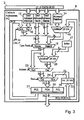
- the main addressing functions performed by the processing unit namely an addressing function 5 to read or write access to the memory of data, a function 6 for determining the value of the program pointer while running a program by the microprocessor, and a function 7 for determine the value of pointers used in the modes indirect addressing.
- the addresses determined by the functions 5, 6, 7 are applied to a multiplexer 25 who selects one of these outputs based on the program instruction being executed.
- this function 5 further comprises a register 32 on one byte, intended to receive the byte of the extended (24-bit) address of the memory location to access, this byte also being associated with the code transfer instruction.
- the output of register 32 is applied to the input of a multiplexer 33 with two inputs, whose other entry is forced to octet 00.
- the output of the register 31 is applied in input of another multiplexer 34, as well as at the input an adder 36 on 16 bits, the other input receives the contents of an index register 17 on a byte, this so that the contents of the registers 31 and 17 be added to obtain a result in two bytes.
- the output of the adder 36 is connected in input of the multiplexer 34, whose output is concatenated with the output of the multiplexer 33, so as to form an address on 3 bytes, which is applied to the input of a multiplexer 35 and another adder 37 of 24 bits, whose other input receives the contents of the registry 17 and whose output is connected to the input of the multiplexer 35.
- the output of the multiplexer 35 corresponds at the exit of function 5.
- the multiplexers 33, 34 and 35 are controlled so as to provide at the output of function 5 the address contained in the register 31 with the extended byte forced to 0.
- multiplexers 33, 34 and 35 are ordered in order to apply the content concatenated registers 31 and 32 at the output of the function 5.
- non-extended indexed addressing mode the content of the index register 17 and added to the contents of the register 31 by the adder 36, the result of the addition is selected by the multiplexer 34 whose output is concatenated with a null byte selected by the multiplexer 33, the address value thus obtained is applied at the output of function 5 by the multiplexer 35.
- Figure 3 shows the function 6 of determining the value of the register containing the program pointer, that is, the address of the next instruction to read in the program memory.
- the processing unit comprises in a conventional manner, registers 11, 12, 14 in which are loaded from the data bus 3 the Jump addresses associated with jump instructions.
- the registers 11, 12 are intended to respectively receive the top and bottom bytes of a jump address in mode absolute or direct.
- the output of these two registers is concatenated and applied to a first multiplexer 18.
- the output of the register 14 intended to receive a jump value in relative addressing mode, for example on one byte is connected via a adder 15 on 24 bits to a second input of the multiplexer 18.
- the output of the multiplexer 18 is connected to another 26-bit adder 26 of which the other input is linked to the index register 17.
- the outputs respective of the multiplexer 18 and the adder 26 are connected to a second multiplexer 23 whose output is connected to the input of a third multiplexer 24.
- the output of the multiplexer 24 is connected to the input of registers 19, 20 containing the low and high bytes of the PC program pointer, the output of these registers constituting the output of function 6.
- This output is looped on one hand on an incrementer 22 of 1 for increment the value of the PC so as to read the following statement in the. current program execution by the microprocessor, and secondly on an input of the adder 15 so that the relative jump value contained in the register 14 can be added to the current value of the pointer program.
- function 6 further comprises a third register 13 associated with registers 11, 12 for containing a jump address, the register 13 being intended to contain the extended byte of the jump address.
- the output of this register is linked to the input of a multiplexer 16 whose output is concatenated with the output of the two other registers 11, 12 before being applied to the input of the multiplexer 18 whose inputs and outputs are 24-bit.
- the registers containing the pointer PC program include a third register 21 intended to contain the extended byte of the program pointer, the this register being on the one hand concatenated with the output of the other two registers 19, 20 of the front PC to be applied at the output of the function 6.
- the output of register 21 is connected to the input of multiplexer 16.
- the respective outputs of the incrementer 22 and the adder 26 are also 24 bits, so as to perform operations incrementing and adding 24-bit.
- the multiplexer 24 is controlled for select the output of the incrementer 22 to which the contents of registers PC 19, 20, 21 is applied, and delivering a PC program pointer value incremented by 1 which is inserted in the registers 19, 20, 21, so as to read the following address in the program memory area. It should be noted that in the case from an old program (working with a space addressable on 16 bits), the value of the register 21 remains at 0 at the output of the incrementer 22.
- the instruction executed is a jump instruction in direct or absolute addressing mode
- such an instruction including an instruction code associated with a word of address there are two cases according to the associated address is on two (direct addressing not extended) or three bytes (extended direct addressing).
- non-extended direct addressing mode multiplexer 16 is controlled to select the current value of register 21 which is concatenated with the output of both registers 11, 12 containing the jump address.
- the multiplexers 18, 23 and 24 are controlled so as to send this concatenated address in the registers 19, 20, 21 of program pointer, which is then sent at the output of the function 6.
- the multiplexer 16 is controlled so as to select the output of the register 13 containing the extended byte of the address of jump, so that it is concatenated with the output of the two other registers 11, 12 containing the low bytes and top of the jump address.
- the extended value of the jump address thus constituted is sent to the PC registers 19, 20, 21 via the multiplexers 18, 23 and 24.
- the value of the jump contained in register 14 is added in the adder 15 to the value of the pointer of program contained in registers 19, 20, 21, the result obtained being on 24 bits.
- the multiplexers 18, 23 and 24 are controlled in order to apply the output of the adder 15 at the input of the registers PC 19, 20, 21. It should be noted that in the case of an old program, the addition made by the adder 15 does not alter the contents of the register 21 which remains at 0. '
- the value of the index register 17 is added during a 24-bit addition made by the adder 26 at the output address of the multiplexer 18, the multiplexers 23 and 24 being controlled for insert the address obtained at the output of the adder 26 in the registers PC 19, 20, 21.
- the size of the index register 17 used in functions 5 and 6 can advantageously be expanded from 8 to 16 bits without changing the structure logic circuits shown in Figures 2 and 3. In Figure 3, the size of this register can even be extended to 24 bits without having to modify the circuit.
- Figures 4 to 6 show three variants of the function 7 which makes it possible to perform calculations of pointers, in order to propose addressing modes indirectly, the values of pointers obtained being then applied at the input of functions 5 or 6.
- this function 7 of pointer calculations is not modified compared to the microprocessors a 16-bit address bus, which implies that all pointers manipulated by the microprocessor according to the invention are placed in non-extended memory zone 2a (addresses from 000000h to 00FFFFh).
- This function includes in a conventional manner two registers 41, 42 of a byte in which the low bytes are inserted respectively and top of the pointer to process.
- the exit of the register 42 is connected to a multiplexer 43 whose the other entry is forced at 00h and the exit is concatenated with the output of the low address register 41.
- the 16-bit concatenated value is applied to a second multiplexer 45 and an incrementer 44 of 16 bits, the output of the incrementer being connected to a other input of the multiplexer 44.
- the output of the multiplexer 44 on 16 bits is concatenated with a null byte to form a 24-bit address.
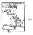
- function 7 shown in FIG. 4 can be modified as shown in Figure 5.
- function 7 includes another incrementer 46 out of 16 bits whose input is connected to the output of the incrementer 44.
- the multiplexer 45 includes a third entrance connected to the exit of the second incrementer 46.
- the multiplexer 45 is controlled to select the address on 16 bits of the extended byte of the pointer that is provided by registers 41 and 42.
- this address is incremented in the incrementer 44 for calculate the address of the high byte of the pointer, and selected by the multiplexer 45.
- the address of the top byte of the pointer is incremented in the incrementer 46 to obtain the address the low byte of the pointer, this value being selected by the multiplexer 45.
- These three addresses 16 bits are successively sent to the bus address 4 after being concatenated with a byte to 00h to be on 24 bits.
- the function 7 represented in FIGS. 4 and 5 handles pointers in the area low memory 2a, that is to say at an address on 1 or 2 bytes.
- this function can still be modified as shown in Figure 6 to be able to access pointers in extended memory 2b, i.e., to a three-byte address.
- the incrementer 44 and possibly 46, as well as the multiplexer 45 must be on 24 bits, the output of the latter directly providing the output of the function 7.
- the respective outputs of the register 41 and multiplexers 43 and 48 are concatenated to form a 24-bit word, which is sent on the multiplexer 45, then on the incrementer 44, then possibly on the incrementer 46.
- the multiplexer 16 ( Figure 3) is controlled so as not to change the extended part PCE of the PC register by the contents of the register 13.
Landscapes
- Engineering & Computer Science (AREA)
- Software Systems (AREA)
- Theoretical Computer Science (AREA)
- Physics & Mathematics (AREA)
- General Engineering & Computer Science (AREA)
- General Physics & Mathematics (AREA)
- Executing Machine-Instructions (AREA)
Description
Claims (10)
- Microprocesseur comprenant une unité de traitement (1), des moyens de connexion et d'accès à un espace mémoire (2) adressable, et des moyens pour exécuter les instructions d'un jeu d'instructions comprenant des instructions d'accès à l'espace mémoire, caractérisé en ce que l'espace mémoire comprend une zone mémoire basse (2a) et une zone mémoire étendue (2b), en ce que le jeu d'instructions comprend un premier ensemble d'instructions comportant des instructions d'accès à la zone mémoire basse (2a), et un second ensemble d'instructions, distinct du premier ensemble d'instructions, et regroupant toutes les instructions donnant accès à la zone mémoire étendue du jeu d'instructions, et en ce que le microprocesseur comprend des moyens pour empêcher tout accès à la zone mémoire étendue tant que le microprocesseur exécute des instructions du premier ensemble d'instructions.
- Microprocesseur selon la revendication 1, caractérisé en ce que chaque emplacement de l'espace mémoire est associé à une adresse respective d'accès, et en ce que le microprocesseur comprend des moyens pour forcer l'adresse d'un emplacement à accéder pour que celle-ci pointe sur un emplacement de la zone mémoire basse (2a), lors de l'exécution d'instructions du premier ensemble d'instructions.
- Microprocesseur selon l'une des revendications 1 et 2, caractérisé en ce que le second ensemble d'instructions comprend uniquement des instructions de saut et d'appel de sous-programme à un emplacement mémoire quelconque de l'ensemble de l'espace mémoire (2), et des instructions de transfert de données entre un emplacement mémoire quelconque de l'ensemble de l'espace mémoire (2) et un registre interne prédéfini du microprocesseur.
- Microprocesseur selon l'une des revendications 1 à 3, caractérisé en ce que chaque emplacement de l'espace mémoire est associé à une adresse respective d'accès, et en ce que pour l'exécution d'instructions de saut ou d'appel de sous-programme du premier ensemble d'instructions, en mode d'adressage direct à partir d'un emplacement en zone mémoire basse (2a), le microprocesseur comprend des moyens pour maintenir l'adresse de l'emplacement de destination du saut pour que celle-ci pointe sur un emplacement de la zone mémoire basse.
- Microprocesseur selon l'une des revendications 1 à 4, caractérisé en ce que le premier ensemble d'instructions comprend des instructions d'adressage en mode indirect pour accéder à un emplacement de la zone mémoire basse (2a), le microprocesseur comprenant des moyens pour forcer l'adresse et la valeur d'un pointeur spécifiant un accès en mode indirect pour que celui-ci soit situé en zone mémoire basse et pointe dans cette zone.
- Microprocesseur selon l'une des revendications 1 à 4, caractérisé en ce que le second ensemble d'instructions comprend des instructions d'accès à la zone mémoire étendue (2b) en mode d'adressage indirect.
- Microprocesseur selon la revendication 6, caractérisé en ce qu'en mode d'adressage indirect dans la zone mémoire étendue (2b), les pointeurs déterminant l'adresse de l'emplacement mémoire à accéder sont situés dans la zone mémoire basse (2a).
- Microprocesseur selon la revendication 6 ou 7, caractérisé en ce qu'en mode d'adressage indirect dans la zone mémoire étendue (2b), les pointeurs déterminant l'adresse de l'emplacement mémoire à accéder sont situés dans la zone mémoire étendue(2b).
- Microprocesseur selon l'une des revendications 1 à 8, caractérisé en ce que qu'il comprend un bus d'adresse (4) conçu pour accéder à l'ensemble de l'espace adressable (2), et un registre de pointeur de programme (19, 20, 21) dont la taille correspond à celle du bus d'adresse pour pouvoir accéder à une instruction de programme à exécuter située à n'importe quel emplacement de l'espace adressable (2).
- Microprocesseur selon l'une des revendications 1 à 9, caractérisé en ce que la zone mémoire basse (2a) est accessible sur 16 bits et la zone mémoire étendue (2b) est accessible sur 24 bits.
Applications Claiming Priority (3)
| Application Number | Priority Date | Filing Date | Title |
|---|---|---|---|
| FR0113478A FR2831289B1 (fr) | 2001-10-19 | 2001-10-19 | Microprocesseur disposant d'un espace adressable etendu |
| FR0113478 | 2001-10-19 | ||
| PCT/FR2002/003481 WO2003034204A1 (fr) | 2001-10-19 | 2002-10-11 | Microprocesseur disposant d'un espace adressable etendu |
Publications (2)
| Publication Number | Publication Date |
|---|---|
| EP1436694A1 EP1436694A1 (fr) | 2004-07-14 |
| EP1436694B1 true EP1436694B1 (fr) | 2005-05-04 |
Family
ID=8868462
Family Applications (1)
| Application Number | Title | Priority Date | Filing Date |
|---|---|---|---|
| EP02801366A Expired - Lifetime EP1436694B1 (fr) | 2001-10-19 | 2002-10-11 | Microprocesseur disposant d'un espace adressable etendu |
Country Status (6)
| Country | Link |
|---|---|
| US (1) | US7370159B2 (fr) |
| EP (1) | EP1436694B1 (fr) |
| JP (1) | JP2005505848A (fr) |
| DE (1) | DE60204036D1 (fr) |
| FR (1) | FR2831289B1 (fr) |
| WO (1) | WO2003034204A1 (fr) |
Families Citing this family (3)
| Publication number | Priority date | Publication date | Assignee | Title |
|---|---|---|---|---|
| EP1622009A1 (fr) * | 2004-07-27 | 2006-02-01 | Texas Instruments Incorporated | Architecture et systèmes JSM |
| US8799617B2 (en) * | 2006-08-01 | 2014-08-05 | Freescale Semiconductor, Inc. | Memory management unit and method of accessing an address |
| US8443168B2 (en) * | 2007-08-17 | 2013-05-14 | O2Micro Inc. | Microcontroller comprising a plurality of registers and instruction modes |
Family Cites Families (6)
| Publication number | Priority date | Publication date | Assignee | Title |
|---|---|---|---|---|
| US5423013A (en) * | 1991-09-04 | 1995-06-06 | International Business Machines Corporation | System for addressing a very large memory with real or virtual addresses using address mode registers |
| US5566308A (en) * | 1994-05-25 | 1996-10-15 | National Semiconductor Corporation | Processor core which provides a linear extension of an addressable memory space |
| US6192476B1 (en) * | 1997-12-11 | 2001-02-20 | Sun Microsystems, Inc. | Controlling access to a resource |
| US6349380B1 (en) * | 1999-03-12 | 2002-02-19 | Intel Corporation | Linear address extension and mapping to physical memory using 4 and 8 byte page table entries in a 32-bit microprocessor |
| US7171543B1 (en) * | 2000-03-28 | 2007-01-30 | Intel Corp. | Method and apparatus for executing a 32-bit application by confining the application to a 32-bit address space subset in a 64-bit processor |
| US20030204745A1 (en) * | 2002-04-29 | 2003-10-30 | International Business Machines Corporation | Method and system for protecting a processing system from a buffer overflow attack |
-
2001
- 2001-10-19 FR FR0113478A patent/FR2831289B1/fr not_active Expired - Fee Related
-
2002
- 2002-10-11 EP EP02801366A patent/EP1436694B1/fr not_active Expired - Lifetime
- 2002-10-11 JP JP2003536868A patent/JP2005505848A/ja active Pending
- 2002-10-11 WO PCT/FR2002/003481 patent/WO2003034204A1/fr not_active Ceased
- 2002-10-11 DE DE60204036T patent/DE60204036D1/de not_active Expired - Lifetime
-
2004
- 2004-03-31 US US10/814,823 patent/US7370159B2/en not_active Expired - Lifetime
Also Published As
| Publication number | Publication date |
|---|---|
| US20040243786A1 (en) | 2004-12-02 |
| US7370159B2 (en) | 2008-05-06 |
| FR2831289A1 (fr) | 2003-04-25 |
| FR2831289B1 (fr) | 2004-01-23 |
| JP2005505848A (ja) | 2005-02-24 |
| DE60204036D1 (de) | 2005-06-09 |
| EP1436694A1 (fr) | 2004-07-14 |
| WO2003034204A1 (fr) | 2003-04-24 |
Similar Documents
| Publication | Publication Date | Title |
|---|---|---|
| BE1001068A4 (fr) | Methode d'ouverture rapide de fichiers a disques identifies par la denomination de chemins. | |
| FR2489555A1 (fr) | Systeme de traitement de donnees a commande par pipeline | |
| EP0006478A1 (fr) | Dispositif programmable de verrouillage de signaux de commande dans un système de traitement de données | |
| EP2453356A1 (fr) | Procédé, programme d'ordinateur et dispositif de sécurisation de code intermédiaire de programmation pour son exécution par une machine virtuelle | |
| FR3055992A1 (fr) | Gestion d'index dans une memoire flash | |
| EP3314420B1 (fr) | Procédé d'exécution d'un programme d'ordinateur comportant une fonction paramétrée | |
| EP1175122A1 (fr) | Dispositif de gestion de mémoire permettant l'inscription de blocs de données par substitution | |
| EP1436694A1 (fr) | Microprocesseur disposant d'un espace adressable etendu | |
| FR2733065A1 (fr) | Procede et circuit de lecture anticipee d'instrutions/ donnees utilisant un cache de lecture anticipee non consulte | |
| EP0950957B1 (fr) | Procédé pour accéder indifféremment en mode d'adressage physique et en mode d'adressage virtuel à une même zone mémoire de machine de traitement numérique et machine mettant en oeuvre ce procédé | |
| EP1433065A1 (fr) | Procede et dispositif de verificateur de code optimise | |
| FR2587519A1 (fr) | Agencement de changement de mode permettant de changer selectivement des modes d'exploitation d'un systeme de machine virtuelle | |
| EP0733977B1 (fr) | Système informatique avec mémoires hiérarchisées | |
| EP1596282A2 (fr) | Dispositif et procédé de gestion d'un jeu d'instructions d'un microprocesseur | |
| US5765220A (en) | Apparatus and method to reduce instruction address storage in a super-scaler processor | |
| FR2655446A1 (fr) | Dispositif pour transferer des donnees. | |
| EP3244300B1 (fr) | Procédé et outil de génération d'un code programme configuré pour effectuer une vérification du flot de contrôle d'un autre code programme contenant des instructions de branchements indirects | |
| EP1176504B1 (fr) | Procédé de mémorisation comprimée d'un programme | |
| FR2774787A1 (fr) | Procede de stockage et de lecture de mots binaires dans une memoire | |
| FR2898704A1 (fr) | Protection d'un programme contre un deroutement | |
| FR2727538A1 (fr) | Processeur pipeline | |
| EP3792771A1 (fr) | Test de programme | |
| FR2783065A1 (fr) | Procede de compression de code interpretable | |
| FR2820223A1 (fr) | Microprocesseur comprenant des moyens de gestion et d'acces a un espace adressable pagine | |
| EP3489834A1 (fr) | Système informatique, procédé d'accès à un fichier informatique et programme d'ordinateur correspondant |
Legal Events
| Date | Code | Title | Description |
|---|---|---|---|
| PUAI | Public reference made under article 153(3) epc to a published international application that has entered the european phase |
Free format text: ORIGINAL CODE: 0009012 |
|
| 17P | Request for examination filed |
Effective date: 20040406 |
|
| AK | Designated contracting states |
Kind code of ref document: A1 Designated state(s): AT BE BG CH CY CZ DE DK EE ES FI FR GB GR IE IT LI LU MC NL PT SE SK TR |
|
| GRAP | Despatch of communication of intention to grant a patent |
Free format text: ORIGINAL CODE: EPIDOSNIGR1 |
|
| RBV | Designated contracting states (corrected) |
Designated state(s): DE FR GB IT |
|
| GRAS | Grant fee paid |
Free format text: ORIGINAL CODE: EPIDOSNIGR3 |
|
| RAP1 | Party data changed (applicant data changed or rights of an application transferred) |
Owner name: STMICROELECTRONICS S.A. |
|
| GRAA | (expected) grant |
Free format text: ORIGINAL CODE: 0009210 |
|
| AK | Designated contracting states |
Kind code of ref document: B1 Designated state(s): DE FR GB IT |
|
| PG25 | Lapsed in a contracting state [announced via postgrant information from national office to epo] |
Ref country code: IT Free format text: LAPSE BECAUSE OF FAILURE TO SUBMIT A TRANSLATION OF THE DESCRIPTION OR TO PAY THE FEE WITHIN THE PRESCRIBED TIME-LIMIT;WARNING: LAPSES OF ITALIAN PATENTS WITH EFFECTIVE DATE BEFORE 2007 MAY HAVE OCCURRED AT ANY TIME BEFORE 2007. THE CORRECT EFFECTIVE DATE MAY BE DIFFERENT FROM THE ONE RECORDED. Effective date: 20050504 |
|
| REG | Reference to a national code |
Ref country code: GB Ref legal event code: FG4D Free format text: NOT ENGLISH |
|
| REG | Reference to a national code |
Ref country code: IE Ref legal event code: FG4D Free format text: LANGUAGE OF EP DOCUMENT: FRENCH |
|
| REF | Corresponds to: |
Ref document number: 60204036 Country of ref document: DE Date of ref document: 20050609 Kind code of ref document: P |
|
| PG25 | Lapsed in a contracting state [announced via postgrant information from national office to epo] |
Ref country code: DE Free format text: LAPSE BECAUSE OF FAILURE TO SUBMIT A TRANSLATION OF THE DESCRIPTION OR TO PAY THE FEE WITHIN THE PRESCRIBED TIME-LIMIT Effective date: 20050805 |
|
| GBT | Gb: translation of ep patent filed (gb section 77(6)(a)/1977) |
Effective date: 20050822 |
|
| PLBE | No opposition filed within time limit |
Free format text: ORIGINAL CODE: 0009261 |
|
| STAA | Information on the status of an ep patent application or granted ep patent |
Free format text: STATUS: NO OPPOSITION FILED WITHIN TIME LIMIT |
|
| 26N | No opposition filed |
Effective date: 20060207 |
|
| PGFP | Annual fee paid to national office [announced via postgrant information from national office to epo] |
Ref country code: GB Payment date: 20100928 Year of fee payment: 9 |
|
| PGFP | Annual fee paid to national office [announced via postgrant information from national office to epo] |
Ref country code: FR Payment date: 20111118 Year of fee payment: 10 |
|
| GBPC | Gb: european patent ceased through non-payment of renewal fee |
Effective date: 20111011 |
|
| PG25 | Lapsed in a contracting state [announced via postgrant information from national office to epo] |
Ref country code: GB Free format text: LAPSE BECAUSE OF NON-PAYMENT OF DUE FEES Effective date: 20111011 |
|
| REG | Reference to a national code |
Ref country code: FR Ref legal event code: ST Effective date: 20130628 |
|
| PG25 | Lapsed in a contracting state [announced via postgrant information from national office to epo] |
Ref country code: FR Free format text: LAPSE BECAUSE OF NON-PAYMENT OF DUE FEES Effective date: 20121031 |