Technical Field
The present invention relates to an electrostatic chuck
used mainly in the semiconductor industry, and particularly to
an electrostatic chuck which is thin, has small heat capacity
and is excellent in the temperature rising/dropping property.
Background Art
Semiconductors are very important products necessitated
by various industries. Semiconductor chips are produced, for
example, by first preparing a silicon wafer by slicing silicon
single crystal at a predetermined thickness and then forming
a plurality of integrated circuits and the like on the silicon
wafer.
In the production process of semiconductor chips as
described above, a semiconductor wafer such as a silicon wafer
and the like is set on a device which allows various types of
processing of the semiconductor wafer, and subjected to various
types of processing including etching, CVD and the like, whereby
integrated circuits, elements and the like are formed thereon.
When a semiconductor wafer is subjected to suchprocessing,
the semiconductor wafer must be firmly fixed to the device. For
this reason, an electrostatic chuck inside of which electrostatic
electrodes for attracting and firmly holding a semiconductor
wafer are provided is generally employed.
As materials for constituting an electrostatic chuck,
oxide ceramics such as alumina or nitride ceramics are used.
In the case of an electrostatic chuck using ceramics as described
above, electrostatic electrodes are formedonaceramic substrate
and a thin dielectric film is formed on each electrostatic
electrode, so that the semiconductor wafer is adsorbed to the
ceramic substrate by Coulomb force through the dielectric film.
In case that the hot CVD and the like is performed, as
the semiconductor wafer needs to be heated, the electrostatic
chuck is generally provided with a means for heating the ceramic
substrate, such as a resistance heating element and the like.
In the electrostatic chuck using ceramics as described
above, as Young's modulus (strength) thereof is relatively large
even at a high temperature, the thickness of the ceramic substrate
can be made relatively thin and thus the weight of the
electrostatic chuck can be characteristically reduced.
Summary of the Invention
However, in recent years, as the size of semiconductor
wafer becomes larger and the area of a ceramic substrate
inevitably increases, the heat capacity of electrostatic chuck
is getting higher. As a result, the temperature of a ceramic
substrate is less likely to promptly follow the change in the
voltage or current amount and the rate of temperature
rising/dropping is slowed, whereby there arose a problem that
the productivity of semiconductor wafers and the like is
deteriorated.
Further, when a ceramic substrate of a relatively large
size whose diameter exceeds 300 mm is used in order to adapt
to a semiconductor wafer of 12 inches, the temperature tends
to drop exceedingly at the periphery of the ceramic substrate,
whereby there arose a problem that the temperature distribution
on the heating face of the ceramic substrate is not even.
The present invention has been contrived in order to solve
the above-mentioned problems. That is, one object of the present
invention is to provide an electrostatic chuck which allows
sufficiently rapid temperature rising/droppingthereof,in case
that the diameter of a ceramic substrate exceeds 190 mm, or
especially even in case that the diameter of the ceramic substrate
is quite large, exceeding 300 mm.
As a result of the assiduous study for achieving the
above-mentioned object, the inventors of the present invention
have discovered that the temperature rising/dropping properties
of a ceramic substrate can be prevented from deteriorating by
reducing the thickness of the ceramic substrate to 20 mm or less
and also reducing the heat capacity of the ceramic substrate.
The present invention has been completed on the basis of this
discovery.
That is, in a first aspect of the present invention, an
electrostatic chuck comprises: a ceramic substrate equipped with
a temperature controlling means; an electrostatic electrode
formed on the ceramic substrate; and a ceramic dielectric film
provided on the above-mentioned electrostatic electrode,
wherein: the above-mentioned ceramic substrate has a diameter
exceeding 190 mm and a thickness of 20 mm or less; and the
above-mentioned ceramic dielectric film contains oxygen in an
amount of 0.1 to 20 weight %.
According to the electrostatic chuck of the first aspect
of the present invention, by reducing the thickness of the ceramic
substrate to 20 mm or less, the temperature dropping at the
peripheral portion of the ceramic substrate can be made as small
as possible and the heat capacity thereof can be made small,
even in case that the ceramic substrate has a relatively large
size and the diameter thereof exceeds 190 mm. As a result, an
electrostatic chuck which allows rapid temperature
rising/dropping thereof can be realized.
When a ceramic substrate has a relatively large diameter,
the ceramic substrate tends to deflect due to its own weight
and thus a clearance is likely to be generated between the
semiconductor wafer and the ceramic substrate, whereby heating
of the semiconductor wafer evenly becomes difficult to be
performed. Also, the thinner the substrate is, the more the
substrate deflects.
However, in the above-mentioned ceramic dielectric film,
as the dielectric film contains oxygen in an amount of 0.1 to
20 weight %, rigidity of the dielectric film is improved so that
the magnitude of flexure can be reduced.
In the electrostatic chuck of the first aspect of the
present invention, it is preferable to use a resistance heating
element as the above-mentioned temperature controlling means,
because a resistance heating element can be formed in the
electrostatic chuck relatively easily by: coating a conductor
containing paste to a green sheet or a sinteredbody and subj ecting
the resultant to heating and firing; or embedding a metal wire
in a formed body and subjecting the resultant to firing.
In a second aspect of the present invention, an
electrostatic chuck comprises:a ceramicsubstrate equipped with
a temperature controlling means; an electrostatic electrode
formed on the ceramic substrate; and a ceramic dielectric film
provided on the above-mentioned electrostatic electrode,
wherein the above-mentioned ceramic substrate has a diameter
exceeding 300 mm and a thickness of 20 mm or less.
In a case of a large type ceramic substrate whose diameter
exceeds 300 mm, the area of the side face of the periphery thereof
is relatively large and heat is easily lost there by being brought
into contact with air. As a result, the temperature drop at the
periphery of the ceramic substrate is large.
However, in the electrostatic chuck of the second aspect
of the present invention, the thickness of the substrate is
adjusted to 20 mm or less so that the contact area where the
side face of the substrate is brought into contact with air
decreases and heat is less likely to be released there and hence
the temperature dropping at the peripheral portion can be made
small. Also, the thickness of the substrate is adjusted to 20
mm or less so that the heat capacity thereof is made small. Thus,
an electrostatic chuck which makes rapid temperature
rising/dropping thereof possible is realized.
In the electrostatic chuck of the second aspect of the
present invention, the above-mentioned ceramic dielectric film
preferably contains oxygen in an amount of 0.1 to 20 weight %.
In case that the diameter of a ceramic substrate exceeds
300 mm, when the thickness of the substrate is made 20 mm or
less, the ceramic substrate tends to deflect due to its own weight
and thus a clearance is likely to be generated between the
semiconductor wafer and the ceramic substrate, whereby even
heating of the semiconductor wafer may become difficult to be
performed and/or the chucking force may undesirably disperse.
However, by setting the content of oxygen in the ceramic
dielectric film in a range of 0.1 to 20 weight %, rigidity of
the substrate is improved and thus the magnitude of flexure can
be reduced.
Further, in the electrostatic chuck of the second aspect
of the present invention, it is preferable to use a resistance
heating element as the above-mentioned temperature controlling
means, because a resistance heating element can be formed in
the electrostatic chuck re lat i vely easily by: coating a conductor
containing paste to a green sheet or a sinteredbody and subjecting
the resultant to heating and firing; or embedding a metal wire
in a formed body and subjecting the resultant to firing.
Yet further, in the electrostatic chuck of the second
aspect of the present invention, the thickness of the
above-mentioned ceramic dielectric film is preferably in a range
of 50 to 5000 µm. When the thickness of the ceramic dielectric
film is within in the above-mentioned range, the magnitude of
flexure of the ceramic substrate can be reduced.
Incidentally, the publication of JP Kokai Hei 4-304942
discloses an electrostatic chuck which comprises a ceramic
substratewhose thickness is 10 mmanddiameter is 150 mm. However,
in the case of this reference, the problem which the present
invention tries to solve does not occur at all because the diameter
of the substrate is quite small.
Also, the publication of JP Kokai Hei 7-86379 discloses
an electrostatic chuck which includes a ceramic substrate whose
thickness is 5 mm and diameter is 210 mm. However, in the case
of this reference, the ceramic substrate thereof does not have
sufficient rigidity because the content of yttria in the
substrate is 2 weight % and this is small. As a result, the chucking
force disperses in the electrostatic chuck.
Further, the publication of JP Kokai Hei 10-72260 discloses
a ceramic substrate whose diameter is 200 mm and thickness is
12 mm. However, this reference makes no description of the oxygen
content of the ceramic substrate.
In short, the above-mentioned references of the prior art
are all related to a substrate whose diameter is smaller than
300 mm and irrelevant to the problem of temperature dropping
at the periphery of the substrate.
Brief Description of Drawings
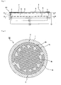
Fig. 1 is a longitudinal sectional viewwhich schematically
shows one example of an electrostatic chuck according to the
first and the second aspects of the present invention.
Fig. 2 is a sectional view taken along the A-A line of
the electrostatic chuck shown in Fig. 1.
Fig. 3 is a sectional view taken along the B-B line of
the electrostatic chuck shown in Fig. 1.
Fig. 4 is a longitudinal sectional viewwhich schematically
shows one example of an electrostatic chuck according to the
first and the second aspects of the present invention.
Fig. 5 is a longitudinal sectional viewwhich schematically
shows one example of an electrostatic chuck according to the
first and the second aspects of the present invention.
Fig. 6 is a longitudinal sectional viewwhich schematically
shows one example of an electrostatic chuck according to the
first and the second aspects of the present invention.
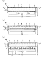
Figs. 7 (a) to 7 (d) are longitudinal sectional views which
schematically shows some steps of the production process of an
electrostatic chuck according to the first and the second aspects
of the present invention.
Fig. 8 is a horizontal sectional views schematically
showing one example of electrostatic electrodes which constitute
an electrostatic chuck according to the first and the second
aspects of the present invention.
Fig. 9 is a horizontal sectional views schematically
showing one example of electrostatic electrodes which constitute
an electrostatic chuck according to the first and the second
aspects of the present invention.
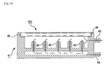
Fig. 10 is a sectional views which schematically shows
an electrostatic chuck according to the first and the second
aspects of the present invention in a state in which the
electrostatic chuck is fixed in a supporting case.
Explanation of Numerals
- 2, 22, 32a, 32b
- chuck positive electrostatic layer
- 2a, 3a
- semicircular arc part
- 2b, 3b
- combteeth-shaped part
- 3, 23, 33a, 33b
- chuck negative electrostatic layer
- 4
- ceramic dielectric film
- 5
- resistance heating element
- 6
- external terminal pin
- 7
- metal wire
- 8
- Peltier device
- 9
- silicon wafer
- 11
- bottomed hole
- 12
- through hole
- 15
- resistance heating element
- 16, 17
- conductor-filled through hole
- 20, 30, 101
- electrostatic chuck
- 41
- supporting case
- 42
- coolant outlet
- 43
- inhalation duct
- 44
- coolant inlet
- 45
- heat insulator
- 81
- thermocouple
- 82
- ceramic substrate
Detailed Description of the Invention
First, an electrostatic chuck according to the first aspect
of the present invention will be described with reference to
the drawings.
In the first aspect of the present invention, an
electrostatic chuck comprises: a ceramic substrate equipped with
a temperature controlling means; an electrostatic electrode
formed on the ceramic substrate; and a ceramic dielectric film
provided on the above-mentioned electrostatic electrode,
wherein: the above-mentioned ceramic substrate has a diameter
exceeding 190 mm and a thickness of 20 mm or less; and the
above-mentioned ceramic dielectric film contains oxygen in an
amount of 0.1 to 20 weight %.
Fig. 1 is a longitudinal sectional viewwhich schematically
shows one embodiment of an electrostatic chuck according to the
first aspect of the present invention. Fig. 2 is a sectional
view taken along the A-A line of the electrostatic chuck shown
in Fig. 1. Fig. 3 is a sectional view taken along the B-B line
of the electrostatic chuck shown in Fig. 1.
In this electrostatic chuck 101, a chuck positive
electrostatic layer 2 having a semicircular arc part 2a and a
combteeth-shapedpart2bandachucknegativeelectrostaticlayer
3 having a semicircular arc part 3a and a combteeth-shaped part
3b are formed on the surface of a disc-shaped ceramic substrate
1 in the manner that the two electrostatic layers face each other
and the combteeth-shaped portion 2b and the combteeth-shaped
portion 3b cross each other. A thin ceramic dielectric film 4
is further formed on the ceramic substrate 1 which contains the
electrostatic electrodes.
The chuck positive electrostatic layer 2 and the chuck
negative electrostatic layer 3 are connected to the positive
side and the negative side of a direct power source, respectively,
so that a direct current voltage V2 is applied thereto. A silicon
wafer 9 is set on this electrostatic chuck 101 and grounded.
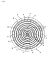
On the other hand, a resistance heating element 5 having
concentric circles-like shape as shown in Fig. 3 as viewed from
the above is provided inside the ceramic substrate 1, so that
the temperature of the silicon wafer 9 is controlled by the
resistance heating element 5. An external terminal pin 6 is
connected and fixed to each end of the resistance heating element
5, so that a voltage V1 is applied to each end of the resistance
heating element 5. Further, although not shown in Figs. 1 and
2, bottomed holes 11 to each of which a temperature measuring
element is inserted and through holes 12 through each of which
a lifter pin (not shown) for supporting and vertically moving
the silicon wafer 9 is inserted, are formed in the ceramic
substrate 1. The resistance heating element 5 may be formed on
the bottom face of the ceramic substrate.
In the above-mentioned structure, when a direct current
voltage V2 is applied between the chuck positive electrostatic
layer 2 and the chuck negative electrostatic layer 3, the silicon
wafer 9 is adsorbed and fixedly held by the ceramic dielectric
film 4, due to the electrostatic action (Coulomb force) between
the chuck positive electrostatic layer 2 and the chuck negative
electrostatic layer 3.
The diameter of the ceramic substrate which constitutes
the electrostatic chuck of the first aspect of the present
invention exceeds 190 mm, this is because the electrostatic chuck
can cope with a silicon wafer of large size. The diameter of
the above-mentioned ceramic substrate is preferably 200 mm or
more, and more preferably larger than 200 mm. It is especially
preferable that the diameter of the ceramic substrate is 300
mm or larger, in terms of well coping with a semiconductor wafer
of the next generation.
The thickness of the above-mentioned ceramic substrate
is to be 20 mm or less, and preferably 10 mm or less. This is
to reduce the heat capacity of the electrostatic chuck by making
the electrostatic chuck thinner, to cope with the enlargement
of the size of the electrostatic chuck. When the diameter of
a ceramic substrate is 300 mm or more, the area of the periphery
becomes larger and thus the contact area at which the ceramic
substrate is brought into contact with the atmospheric gas such
as air becomes larger, whereby the temperature significantly
drops at the peripheral portion of the substrate. Therefore,
the above-mentioned contact area is reduced by decreasing the
thickness of the ceramic substrate, so that the temperature
dropping at the peripheral portion is prevented.
Especially, by setting the thickness of the substrate to
10 mm or less, the temperature dropping property is improved.
It is particularly preferable that the thickness of the ceramic
substrate is within a range of 1 to 5 mm because the dispersion
of the temperature on the heating face is decreased.
As described above, the ceramic dielectric film which
constitutes the electrostatic chuck of the first aspect of the
present invention contains oxygen in an amount of 0.1 to 20
weight %.
The thinner the substrate is, the more the substrate
deflects. However, by incorporating the oxygen in a range of
0.1 to 20 weight %, the rigidity of the substrate is improved
and the magnitude of fluxure thereof can be decreased.
The electrostatic chuck of the first aspect of the present
invention has the above-mentioned structure and is realized,
for example, in the embodiment as shown in Figs. 1 to 3.
Hereinafter, each of the members which constitute the
above-mentioned electrostatic chuck, as well as other
embodiments and the like of the electrostatic chuck of the first
aspect of the present invention, will be described one by one
in detail.
The ceramic dielectric film which constitutes the
electrostatic chuck of the first aspect of the present invention
is provided in a manner that the electrostatic electrodes formed
on the ceramic substrate are covered by the ceramic dielectric
film.
The ceramic material which constitutes this ceramic
dielectric film is not particularly restricted, and examples
thereof include nitride ceramic, carbide ceramic, oxide ceramic
and the like.
Examples of the above-mentioned nitride ceramic include
metal nitride ceramic such as aluminum nitride, silicon nitride,
boron nitride, titanium nitride and the like.
Examples of the above-mentioned carbide ceramic include
metal carbide ceramic such as silicon carbide, zirconium carbide,
titanium carbide, tantalum carbide, tungsten carbide and the
like.
Examples of the above-mentioned oxide ceramic include
metal oxide ceramic such as alumina, zirconia, cordierite,
mullite and the like.
These examples of ceramic may be used solely or in a
combination of two or more of them.
Among these examples of ceramic, nitride ceramic and
carbide ceramic are more preferable than oxide ceramic because
the thermal conductivity of nitride ceramic and that of carbide
ceramic is higher than that of oxide ceramic.
Among the examples of the nitride ceramic, aluminumnitride
is the most preferable because the thermal conductivity thereof ,
which is 180 W/m·K, is the highest in the nitride ceramics.
It is preferable that the above-mentioned ceramic
dielectric film contains oxygen in an amount of 0.1 to 20 weight %.
When the content of oxygen in the ceramic dielectric film is
less than 0.1 weight %, a sufficient breakdown voltage cannot
be ensured. On the other hand, when the content of oxygen in
the ceramic dielectric film exceeds 5 weight %, the breakdown
voltage drops due to the deterioration of the high breakdown
voltage property of the oxides at a high temperature. Further,
when the content of oxygen in the ceramic dielectric film exceeds
20 weight %, the temperature rising/dropping property of the
ceramic substrate deteriorates due to the drop in the thermal
conductivity.
Firing is carried out: after heating the raw material
powder of the nitride ceramic, the carbide ceramic and the like
as described above in the air or oxygen gas; or after mixing
the above-mentioned raw material powder with metal oxides, in
order to incorporate oxygen in the above-mentioned nitride
ceramic or the carbide ceramic and the like.
Examples of the above-mentioned metal oxide include yttria
(Y2O3), alumina (Al2O3), rubidium oxide (Rb2O), lithium oxide
(Li2O), calcium carbonate (CaCO3) and the like.
It is preferable that 1 to 20 parts by weight of the metal
oxide as described above is added to 100 parts by weight of the
nitride ceramic.
The above-mentioned dielectric film may be composed of
silicon carbide which contains B, C, Be, BeO and the like as
the sintering aid, because such a dielectric film exhibits high
mechanical strength and excellent heat resistance.
The above-mentioned ceramic dielectric film desirably
contains carbon. In case that the thermal conductivity of the
ceramic dielectric film at a high temperature (approximately
500 °C) is to be prevented from decreasing, it is preferable
that crystalline carbon is added to the ceramic dielectric film.
In case that the volume resistivity of the ceramic dielectric
film at a high temperature is to be prevented from decreasing,
it is preferable that amorphous carbon is added to the ceramic
dielectric film. Accordingly, depending on the application, both
the volume resistivity and the thermal conductivity can be
simultaneously adjusted in an appropriate manner by adding both
crystalline carbon and amorphous carbon threto.
The crystallinity of carbon can be determined by analyzing
the magnitude of peaks in the vicinities of 1550 cm-1 and 1333
cm-1 obtained when Raman spectrum is measured.
When the ceramic dielectric film contains carbon, the
content of carbon contained in the ceramic dielectric film is
preferably in a range of 5 to 5000 ppm. When the content of carbon
in the ceramic dielectric film is less than 5 ppm, radiant heat
is decreased and there arises difficulty in concealing the
electrostatic electrodes. On the other hand, when the content
of carbon in the ceramic dielectric film exceeds 5000 ppm, the
ceramic dielectric film can no longer be made dense and there
arises difficulty in suppressing drop in the volume resistivity.
The content of carbon in the ceramic dielectric film is most
preferably in a range of 100 to 2000 ppm.
In order to make the carbon contained in the ceramic
dielectric film into amorphous one, a resin or hydrocarbons and
the like which are less likely to become crystalline by heating
may be added at the time of producing a formed body by mixing
the raw material powder, a resin, a solvent and the like together,
thus the formed body is degreased in an atmosphere which contains
relatively little oxygen or a non-oxidizing atmosphere.
Alternatively, it is acceptable to produce amorphous carbon by
heating a hydrocarbon such as saccharose and the like or a resin
which are easily made amorphous by heating and then adding the
obtained amorphous carbon to the ceramic dielectric film. In
case that crystalline carbon is to be added to the ceramic
dielectric film, graphite which has been made powdery by
pulverizing or crystalline carbon black can be used.
Further, as the decomposing rate of an acrylic resin binder
varies depending on the acid value thereof, it is possible to
adjust the amount of carbon or crystallinity, to some extent,
by changing the acid value of the acrylic resin binder.
The thickness of the above-mentioned ceramic dielectric
film is preferably in a range of 50 to 5000 µm. When the thickness
of the above-mentioned ceramic dielectric film is less than 50
µm, a sufficient breakdown voltage cannot be obtained because
the dielectric film is too thin, whereby there is a possibility
that the ceramic dielectric film suffers from dielectric
breakdown when a silicon wafer is set and adsorbed thereon. In
addition, when the thickness of the ceramic dielectric film is
less than 50 µm, the stiffness of the ceramic dielectric film
is not sufficient, whereby f luxure of the above-mentioned ceramic
substrate cannot be prevented. On the other hand, when the
thickness of the ceramic dielectric film exceeds 5000 µm, the
distance between the silicon wafer and the electrostatic
electrodes is so large that the capacity of attracting the silicon
wafer is deteriorated. Accordingly, the thickness of the ceramic
dielectric film is more preferably in a range of 50 to 1500 µm.
It is preferable that the porosity of the above-mentioned
ceramic dielectric film is 5 % or less and the diameter of the
largest pore is 50 µm or less.
When the above-mentioned porosity exceeds 5 %, the number
of the pores present in the ceramic dielectric film increases
and the diameter of the pores becomes too large. As a result,
the pores are likely to communicate with each other and the
breakdown voltage tends to drop in the ceramic dielectric film
of such a structure.
On the other hand, when the diameter of the largest pore
exceeds 50 µm, the ratio of the pore diameter with respect to
the thickness of the ceramic dielectric film, as well as the
proportion of the pores which are communicated with each other,
is increased, whereby the breakdown voltage tends to drop.
The porosity is more preferably 0, or 3 % or less and the
diameter of the largest pore is more preferably 0, or 10 µm or
less.
The porosity and the diameter of the largest pore are
adjusted by the length of pressurizing time, the pressure, the
temperature during the sintering process and the amount of the
additives such as SiC, BN. SiC or BN inhibits the sintering
process, thereby facilitating introduction of pores to the
ceramic dielectric film.
Measurement of the diameter of the largest pore is carried
out by: preparing five samples; grinding the surface of each
sample into the mirror plane; photographing the surface of each
sample at ten sites by an electron microscope with 2000 to 5000
magnifications; measuring the diameter of the largest pore in
each shot; and calculating the average of the diameters of the
largest pores of 50 shots.
The porosity is measured by Archimedes' method which
includes the steps of: pulverizing the sintered body; mixing
the pulverized material with an organic solvent or mercury and
measuring the volume of the pulverized material; obtaining the
true specific gravity of the pulverized material from the weight
and the volume of the pulverized material; and calculating the
porosity from the true specific gravity and the apparent gravity
of the sintered body.
The ceramic dielectric film may include pores to some
extent as described above, because the presence of an acceptable
number of open pores at the surface of the ceramic dielectric
film facilitates smooth dechucking.
Examples of the electrostatic electrodes formed on the
ceramic substrate include a sintered body of metal or conductive
ceramic, metal foils and the like. The metal sintered body is
preferably made of at least one kind of metal selected from
tungsten and molybdenum. The metal foils are preferably made
of the same material as the metal sintered body, because these
metals are relatively less likely to be oxidized and have
sufficient conductivity as an electrode. As the conductive
ceramic, at least one kind selected from the group consisting
of carbide of tungsten and carbide of molybdenum can be used.
Examples of the material of the ceramic substrate used
in the electrostatic chuck of the first aspect of the present
invention include nitride ceramic, carbide ceramic, oxide
ceramic and the like.
Examples of the above-mentioned nitride ceramic, the
above-mentioned carbide ceramic and the above-mentioned oxide
ceramic as the material of the ceramic substrate include those
raised in the description of the above-mentioned ceramic
dielectric film.
Among these examples of ceramic described above, nitride
ceramic and carbide ceramic are preferable because nitride
ceramic and carbide ceramic have relatively high thermal
conductivity and thus can excellently conduct the heat generated
at the resistance heating element.
It is preferable that the ceramic dielectric film and the
ceramic substrate are made from the same materials, because in
such a case, the production process of the electrostatic chuck
can be easily carried out by laminating green sheets produced
by the same method and firing the lamination in the same condition.
Among the examples of nitride ceramic, aluminum nitride
is the most preferable because the thermal conductivity thereof,
which is 180 W/m·K, is the highest in the nitride ceramics.
The above-mentioned ceramic substrate may include carbon
because carbon contributes to generation of high radiation heat.
The content of carbon in the ceramic substrate is preferably
in a range of 5 to 5000 ppm.
Carbon may be either in the crystalline state, for example
in the form of graphite powder, or in the amorphous state as
is achieved by using a hydrocarbon or a resin which are easily
made amorphous. Alternatively, both of carbon in the crystalline
state and carbon in the amorphous state may be used together.
The ceramic such as nitride ceramic which constitutes the
ceramic substrate preferably contains 0.1 to 20 weight % of metal
oxides therein, as is the case with the ceramic dielectric film.
It is preferable that the porosity of the above-mentioned
ceramic substrate is 5 % or less and the diameter of the largest
pore is 50 µm or less. Further, the porosity is more preferably
0, or 3 % or less and the diameter of the largest pore is 0,
or 10 µm or less.
Figs. 8 and 9 are horizontal sectional views schematically
showing electrostatic electrodes in other types of electrostatic
chuck. In the electrostatic chuck 20 shown in Fig. 8, a chuck
positive electrostatic layer 22 and a chuck negative
electrostatic layer 23 each having a semicircular shape are
formed inside the ceramic substrate 1. In the electrostatic chuck
shown in Fig. 9, a chuck positive electrostatic layer 32a, 32b
and a chuck negative electrostatic layer 33a, 33b each having
a form obtained by equally dividing a circle into four portions,
are formed inside the ceramic substrate 1. The two chuck positive
electrostatic layers 22a, 22b and two chuck negative
electrostatic layer 33a, 33b are formed, such that the two chuck
positive electrostatic layers 22a, 22b and the two chuck negative
electrostatic layers 33a, 33b intersect each other.
The electrostatic chuck may be provided wi th RF electrodes,
and the electrostatic electrodes may be provided on the both
faces of the ceramic substrate.
In case that the electrostatic electrodes are formed such
that the electrostatic electrodes have shapes which would be
obtained by dividing a circular electrode into plural pieces,
the number of the divided pieces is not particularly restricted
and may be five or more, and the shape of the divided pieces
is not restricted to a sector form, either.
In the electrostatic chuck according to the first aspect
of the present invention, a temperature controlling means such
as a resistance heating element is provided, as shown in Fig.
1. The temperature controlling means is provided, because tasks
such as heating the silicon wafer set on the electrostatic chuck
are required during the CVD processing and the like.
Examples of the above-mentioned temperature controlling
means include a Peltier device (refer to Fig. 6), in addition
to the resistanceheating element 5 shown in Fig. 3. The resistance
heating element may be provided either inside the ceramic
substrate or on the bottom face of the ceramic substrate. In
case that the resistance heating element is provided in the
ceramic substrate, a coolant (such as air) outlet and the like
as a cooling means may be provided in the supporting case in
which the electrostatic chuck is fitted.
In case that the resistance heating element is provided
inside the ceramic substrate, the resistance heating element
may be provided in the form of a plurality of layers. In this
case, it is preferable that the patterns at the layers are formed
so that the patterns complement each other, whereby any portion
of the heating face is covered by one of these patterns or layers
without leaving any uncovered portion when viewed from the above.
For example, a structure having a staggered arrangement may be
used.
In case that the resistance heating element is set in the
ceramic substrate, it is preferable that the resistance heating
element is provided at a position which is within 60 % of the
ceramic substrate thickness as measured from the bottom face
of the ceramic substrate, so that heat is well dissipated before
reaching the heating face and the distribution of the temperature
on the heating face is reliably made even.
Examples of the resistance heating element include a
sintered body of metal or conductive ceramic, a metal foil, a
metal wire and the like. As the metal sintered body, a metal
sintered body which is produced by using at least one kind of
element selected from tungsten and molybdenum is preferable,
because these metals are relatively less likely to be oxidized
and have a sufficient resistance value for generating heat.
As the conductive ceramic, at least one kind selected from
carbides of tungsten and molybdenum can be preferably used.
Further, in case that the resistance heating element is
formed on the bottom face of the ceramic substrate, it is
preferable to use rare metal (gold, silver, palladium, platinum)
or nickel for the metal sintered body. Specifically, silver,
silver-palladium can be preferably used.
The shape of the metal particles used for producing the
above-mentioned metal sintered body may be either spherical or
scaly. In case that these metal particles are used, both spherical
particles and scaly particles may be used in a mixed manner.
A metal oxide may be added to the metal sintered body.
The above-mentionedmetal oxide is used in order to tightly adhere
the metal particles to the ceramic substrate. The reason why
the above-mentioned metal oxide improves the adhesion of the
metal particles to the ceramic substrate is not clearly known.
But, a thin oxidized film is formed on the surface of the metal
particle, and an oxidized film is also formed on the surface
of the ceramic substrate, regardless of whether the ceramic
substrate is oxide ceramic or non-oxide ceramic. It is thus
assumed that the oxidized film of the metal particle and that
of the ceramic substrate are combined to one film through the
metal oxide when these oxidized films are sintered on the surface
of the ceramic substrate, whereby the metal particles are closely
adhered to the ceramic substrate.
As the above-mentioned metal oxide, at least one kind of
compound selected from the group consisting of lead oxide, zinc
oxide, silica, boron oxide (B2O3), alumina, yttria and titania
is preferably used, because these oxides can improve adhesion
of the metal particles to the ceramic substrate without
increasing the resistance value of the resistance heating
element.
The content of the metal oxide is preferably in a range
of 0.1 parts by weight or more and less than 10 parts by weight
with respect to 100 parts by weight of the metal particles. By
using the metal oxide within the above-mentioned range, the
adhesion between the metal particles and the ceramic substrate
can be enhancedwithout increasing the resistance value too much.
The contents of lead oxide, zinc oxide, silica, boron oxide
(B2O3), alumina, yttria and titania are preferably 1 to 10 parts
by weight of lead oxide, 1 to 30 parts by weight of silica, 5
to 50 parts by weight of boron oxide, 20 to 70 parts by weight
of zinc oxide, 1 to 10 parts by weight of alumina, 1 to 50 parts
by weight of yttria and 1 to 50 parts by weight of titania, with
respect to the whole weight of the metal oxides expressed as
100 parts by weight. However, it is preferable that these
contents of the metal oxides are adjusted so that the total sum
of the metal oxides does not exceed 100 parts by weight, because
these metal oxides can especially enhance adhesion thereof to
the ceramic substrate in such a range.
In case that the resistance heating element is provided
on the bottom face of the ceramic substrate, the surface of the
resistance heating element 15 is preferably covered with a metal
layer 150 (refer to Fig. 4). As the resistance heating element
15 is a sintered body of metal particles, the resistance heating
element 15 is easily oxidized if it is exposed, and the resistance
value thereof changes due to this oxidization. By covering the
surface of the resistance heating element 15 with a metal layer
150, such oxidization can be prevented.
The thickness of the metal layer 150 is preferably in a
range of 0.1 to 10 µm. When the thickness of the metal layer
is within this range, the oxidization of the resistance heating
element can be prevented without changing the resistance value
of the resistance heating element.
The metal used for the metal layer for covering is not
particularly limited, as long as the metal is non-oxidizable.
Specific examples thereof include at least one element selected
from the group consisting of gold, silver, palladium, platinum
and nickel. Among these examples, nickel is more preferable.
The resistance heating element requires a terminal for connecting
itself to the power source, and this terminal is mounted to the
resistance heating element by using solder. Nickel effectively
prevents the heat dissipation caused by solder. As the connection
terminal, a terminal pin made of Kovar can be used.
In case that the resistance heating element is formed
inside the ceramic substrate, the surface of the resistance
heating element is not oxidized and thus no covering by the metal
layer is required. When the resistance heating element is formed
inside the ceramic substrate, a portion of the surface of the
resistance heating element may be exposed outside of the ceramic
substrate.
In case that the ceramic substrate is produced by: filling
ceramic powder and the like in a mold; producing a formed body;
and firing the obtained formed body thereafter, the resistance
heating element can be disposed by embedding a metal foil or
a metal wire in the formed body.
Preferable examples of the metal foil used as the
resistance heating element include a resistance heating element
produced by conducting a pattern-forming process (such as
etching) to nickel foil or stainless foil.
The metal foils which have been subjected to the
pattern-forming process may be laminated with a resin film and
the like.
Example of the metal wire include a tungsten wire, a
molybdenum wire and the like.
In case that the Peltier device is used as the temperature
controlling means, either heating or cooling can be performed
by the same element by changing the flow direction of the current,
which is advantageous.
The Peltier device 8 is formed by connecting p-type and
n-type thermoelectric elements 81 in series and attaching these
thermoelectric elements 81 to a ceramic plate 82 and the like,
as shown in Fig. 6.
Examples of the Peltier device include the silicon
/germanium-type Peltier device, the bismuth/antimony-type
Peltier device, the lead/tellurium-type Peltier device and the
like.
Examples of the electrostatic chuck according to the first
aspect of the present invention include: an electrostatic chuck
101 having a structure in which, as shown in Fig. 1, the chuck
positive electrostatic layer 2 and the chuck negative
electrostatic layer 3 are formed between the ceramic substrate
1 and the ceramic dielectric film 4 and the resistance heating
element 5 is provided inside the ceramic substrate 1; an
electrostatic chuck 201 having a structure in which, as shown
in Fig. 4, the chuck positive electrostatic layer 2 and the chuck
negative electrostatic layer 3 are formed between the ceramic
substrate 1 and the ceramic dielectric film 4 and the resistance
heating element 15 is provided on the bottom face of the ceramic
substrate 1; an electrostatic chuck 301 having a structure in
which, as shown in Fig. 5, the chuck positive electrostatic layer
2 and the chuck negative electrostatic layer 3 are formed between
the ceramic substrate 1 and the ceramic dielectric film 4 and
a metal wire 7 as a resistance heating element is embedded inside
the ceramic substrate 1; and an electrostatic chuck 401 having
a structure in which, as shown in Fig. 6, the chuck positive
electrostatic layer 2 and the chuck negative electrostatic layer
3 are formed between the ceramic substrate 1 and the ceramic
dielectric film 4 and a Peltier device 8 composed of a
thermoelectric element 81 and a ceramic plate 82 is formed on
the bottom face of the ceramic substrate 1; and the like.
In the first aspect of the present invention, as shown
in Figs. 1 to 5, the chuck positive electrostatic layer 2 and
the chuck negative electrostatic layer 3 are provided between
the ceramic substrate 1 and the ceramic dielectric film 4, and
the resistance heating element 5 and the metal wire 7 are formed
inside the ceramic substrate 1. As a result, connecting portions
(conductor-filled through holes) 16, 17 for connecting these
with the external terminals, are required. The conductor-filled
through holes 16, 17 are formed by filling a metal having a high
melting point such as tungsten paste and molybdenum paste or
a conductive ceramic such as tungsten carbide and molybdenum
carbide.
Here, the diameter of the connecting portions
(conductor-filled through holes) 16, 17 is preferably in a range
of 0.1 to 10 mm, because when the diameter of the connecting
portions is within this range, not only occurrence of
disconnection of the wires but also generation of cracks or
strains can be prevented.
External terminals 6, 18 are connected thereto, by using
the conductor-filled through holes as connection pads (refer
to Fig. 7(d)).
Such connection is performed by using solder or brazing
filler metal. As the brazing filler metal, silver braze,
palladium braze, aluminum braze and gold braze are preferable.
As the gold braze, Au-Ni alloy is preferable because Au-Ni alloy
exhibits excellent adhesion property to tungsten.
The ratio of Au/Ni is preferably [81.5 to 82.5
(weight %)]/[18.5 to 17.5 (weight %)].
The thickness of the Au-Ni layer is preferably in a range
of 0.1 to 50 µm, because the connection property is reliably
obtained when the thickness of the Au-Ni layer is within this
range. In the case of Au-Cu alloy, the alloy exhibits
deterioration when used in a highly vacuumed state of 10-6 to
10-5 Pa at a high temperature in a range of 500 to 1000 °C. On
the other hand, the Au-Ni alloy does not exhibit deterioration
when the alloy is used in such a harsh condition, which is
advantageous. The content of the impurity elements contained
in the Au-Ni alloy is preferably less than 1 parts by weight
when the whole weight of the Au-Ni alloy is expressed as 100
parts by weight.
In the first aspect of the present invention, a
thermocouple maybe embedded in the bottomedhole 12 of the ceramic
substrate 1, according to necessity. In this arrangement, the
temperature of the resistance heating element can be measured
by the thermocouple, so that the temperature of the resistance
heating element can be controlled by changing the voltage and
the current amount on the basis of the obtained data.
The size of the connecting portion of the metal wire of
the thermocouple is preferably the same as or larger than the
strand diameter of each metal wire, but 0.5 mm or less. The heat
capacity of the connecting portion is made small by such a
structure, whereby the temperature is converted into correctly
and rapidly into the current value. As a result, the temperature
controlling property is improved, whereby the temperature
distribution on the heating face of the wafer is kept small.
Examples of the above-mentioned thermocouple include the
K-type, the R-type, the B-type, the S-type, thee-type, the J-type
and the T-type thermocouples, as are raised in JIS-C-1602 (1980).
Fig. 10 is a sectional view which schematically shows a
supporting case 41 in which the electrostatic chuck having a
structure as described above according to the first aspect of
the present invention is fitted.
The supporting case 41 is designed such that the
electrostatic chuck 101 is fitted therein through a heat
insulator 45. In the supporting case 41, coolant outlets 42 are
formed such that the coolant introduced from a coolant inlet
44 is discharged outside from an inhalation duct 43 through the
coolant outlet 42. By the action of this coolant, the
electrostatic chuck 101 can be cooled.
The supporting case maybe structured such that the ceramic
substrate, which has been set on the upper surface of the
supporting case, is fixed to the supporting case by the fixing
member like bolts.
The electrostatic chuck according to the first aspect of
the present invention is preferably used in a temperature range
of 100 to 800 °C.
Next, one example of the method of producing the
electrostatic chuck according to the first aspect of the present
inventionwill be describedwith reference to the sectional views
shown in Figs. 7 (a) to (d).
(1) First, a green sheet 50 is produced by: preparing powder
of ceramic such as oxide ceramic, nitride ceramic and carbide
ceramic, (powder of nitride or carbide ceramic is fired in an
oxidizing atmosphere so that the ceramic powder contains oxygen) ;
mixing the ceramic powder with an auxiliary agent, a binder,
a solvent and the like, thereby preparing a paste; and forming
the paste in a sheet-like form by the doctor blade method and
the like, thereby producing a green sheet 50.
As the above-mentioned ceramic powder, aluminum nitride,
silicon carbide and the like may be used, for example. Further,
a sintering aid such as yttria and carbon may further be added
thereto, according to necessity.
One or plurality of the green sheet 50, which is laminated
on the green sheet having an electrostatic electrode layer
printed body 51 formed thereon, described below, is the layer
which serves as the ceramic dielectric film 4.
In general, it is preferable that the same raw material
is used for the ceramic dielectric film 4 and the ceramic substrate
1, because then the same preferable firing conditions can be
applied to both the ceramic dielectric film 4 and the ceramic
substrate 1 during the firing process thereof since normally,
the ceramic dielectric film 4 and the ceramic substrate 1 are
sintered together in the integrated arrangement. In case that
different raw materials are used for the ceramic dielectric film
4 and the ceramic substrate 1, the ceramic substrate may be
produced first, so that the electrostatic electrode layer is
formed thereon and the ceramic dielectric film is further
provided on the electrostatic electrode layer.
Examples of the binder which is generally used for the
production of an electrostatic chuck include an acrylic binder,
an ethyl cellulose, a butyl cellosolve and polyvinyl alcohol
and the like. At least one kind of binder selected from the
above-mentioned group can be used as the binder for forming the
ceramic subsrate.
As the solvent, at least one kind of solvent selected from
α-terpineol and glycol is preferably used.
A through hole which a lifter pin of the silicon wafer
is pushed through and a concave portion in which thermocouple
is embedded may be optionally formed in the green sheet 50. The
through hole and the concave portion can be formed by punching
and the like.
The thickness of the green sheet 50 is preferably in a
range of 0.1 to 5 mm.
Next, the conductor containing paste which is to serve
as the electrostatic electrode layer or the resistance heating
element is printed on the green sheet 50.
The printing is performed, in consideration of the
shrinking rate of the green sheet 50, so that a desirable aspect
ratio is obtained. As a result, the electrostatic electrode layer
printed body 51 and the resistance heating element layer printed
body 52 are obtained.
The printed body is formed by printing the conductor
containing paste which contains conductive ceramic, metal
particles and the like on the green sheet.
As the conductive ceramic particles contained in the
conductor containing paste, a carbide of tungsten or molybdenum
is the most preferable because such a carbide is less likely
to be oxidized and the heat conductivity thereof is less likely
to drop, as compared with other materials.
Examples of the metal particle include particles of
tungsten, molybdenum, platinum, nickel and the like.
The average particle diameter of the conductive ceramic
particles and the metal particles is preferably in a range of
0.1 to 5 µm. If the particle size is too large or small, it is
difficult to effect printing with such a conductor containing
paste.
As such a conductor containing paste used for the present
invention, a conductor containing paste which is prepared by
mixing: 85 to 97 parts by weight of metal particles or conductive
ceramic particles; 1.5 to 10 parts by weight of at least one
kind of binder selected from the group consisting of an acrylic
binder, an ethyl cellulose, a butyl cellosolve and polyvinyl
alcohol; 1. 5 to 10 parts by weight of at least one kind of solvent
selected from α-terpineol, glycol, ethyl alcohol and butanol,
is most preferably used.
The conductor containing paste is filled in holes formed
by punching and the like, whereby the conductor-filled through
hole printed bodies 53, 54 are obtained.
Next, as shown in Fig. 7(a), green sheets 50 having the
printed bodies 51, 52, 53, 54 are laminated with the green sheet
50 having no printed body thereon. Several of one of the green
sheet (s) 50 with the above-mentioned structure are/is laminated
on the green sheet on which the electrostatic electrode layer
printed body 51 has been formed. The reason why the green sheet
50, which does not have the printed bodies at the side on which
the resistance heating element is formed, is laminated as
described above, is prevent the end surface of the
conductor-filled through hole from exposing and being oxidized
during firing when the resistance heating element is formed.
If the firing is to be performed, when the resistance heating
element is formed, in a state in which the end surface of the
conductor-filled through hole is exposed, a metal such as nickel
which is less likely to be oxidized needs to be provided therein
by spattering. More preferably, the end surface of the
conductor-filled through hole may be covered by a gold braze
of Au-Ni.
(2) Next, as shown in Fig. 7(b), the lamination is subjected
to heating and pressurizing, whereby the green sheet and the
conductor containing paste are sintered.
The heating temperature is preferably in a range of 1000
to 2000 °C. The pressure for pressurizing is preferably within
a range of 100 to 200 kg/cm2. Heating is performed and pressuring
is conducted in an inactive gas atmosphere. As the inactive gas,
argon, nitrogen and the like may be used, for example. In this
process, the conductor-filled through holes 16, 17, the chuck
positive electrostatic layer 2, the chuck negative electrostatic
layer 3, the resistance heating element 5 and the like are formed.
(3) Next, as shown in Fig. 7 (c), blind holes 13, 14 for connecting
external terminals are formed.
It is preferable that at least a portion of the inner walls
of the blind holes 13, 14 are made conductive and the conductive
inner walls are connected to the chuck positive electrostatic
layer 2, the chuck negative electrostatic layer 3, the resistance
heating element 5 and the like.
(4) Finally, as shown in Fig. 7(d), the external terminals 6,
18 are provided to the blind holes 13, 14 by way of a brazing
filler material such as gold braze and the like. In addition,
a bottomed hole 12 may optionally be formed so that themocouple
can be embedded therein.
As solder, alloys of silver-lead, lead-tin, bismuth-tin
and the like can be used. The thickness of the solder is preferably
in a range of 0.1 to 50 µm. When the thickness of the solder
is within this range, connection by the solder is reliably
conducted in a sufficient manner.
In the above-mentioned example, the electrostatic chuck
101 (refer to Fig. 1) has been described. In case that the
electrostatic chuck 201 (refer to Fig. 4) is to be produced,
a ceramic substrate having an electrostatic electrode layer is
first produced, the conductor containing paste is then printed
on the bottom face of the ceramic substrate, firing is effected
to form a resistance heating element 15, and thereafter a metal
layer 150 is formed by electroless plating and the like. In case
that the electrostatic chuck 301 (refertofig. 5) istobeproduced,
a metal foil and a metal wire as the electrostatic electrode
and the resistance heating element are embedded in the ceramic
powder, at the time of filling the ceramic powder (granules)
in a mold or the like and forming a formed body. The electrostatic
chuck 301 can be produced by sintering the obtained formed body.
Further, in case that the electrostatic chuck 401 (refer
to Fig. 6) is to be produced, a ceramic substrate having an
electrostatic electrode layer is produced and then a Peltier
element is joined to the ceramic substrate by way of a thermal
spraying of metal layer and the like.
Next, an electrostatic chuck according to the second aspect
of the present invention will be described hereinafter.
The second aspect of the present invention is an
electrostatic chuck comprising: a ceramic substrate equipped
with a temperature controlling means; an electrostatic electrode
formed on the ceramic substrate; and a ceramic dielectric film
provided on the electrostatic electrode, wherein the ceramic
substrate has a diameter exceeding 300 mm and a thickness of
20 mm or less.
Figs. 1 to 10 schematically show one example of the
embodiment according to the second aspect of the present
invention.
The ceramic substrate which constitutes the electrostatic
chuck according to the second aspect of the present invention
has diameter exceeding 300 mm, so that the ceramic substrate
can adapt to silicon wafers of larger size and reliably cope
with the semiconductor wafers of the next generation.
The thickness of the above-mentioned ceramic substrate
is set to be 20 mm or less, and desirably 10 mm or less. This
is to reduce the heat capacity of the ceramic substrate by the
decrease in thickness of the ceramic substrate so as to cope
with the enlargement of the size of the electrostatic chuck.
In a case of a ceramic substrate whose diameter exceeding 300
mm, the area of the periphery is relatively large i.e., the area
of the portion at which the ceramic substrate is brought into
contact with an atmospheric gas such as air is relatively large,
whereby the temperature drops significantly at the peripheral
portion of the ceramic substrate. Therefore, in the present
invention, the area of the portion at which the ceramic substrate
is brought into contact with air is decreased by reducing the
thickness of the ceramic substrate, so that the temperature
dropping at the peripheral portion can be prevented.
As the structures of the ceramic substrate, the ceramic
dielectric film, the resistance heating element, the
thermocouple and the like of the electrostatic chuck according
to the second aspect of the present invention are basically the
same as those of the electrostatic chuck according to the first
aspect of the present invention, the detailed description of
the electrostatic chuck according to the second aspect of the
present invention will be omitted.
Further, regarding the method of producing the
electrostatic chuck of the second aspect of the present invention,
the method is basically the same as the method of producing the
electrostatic chuck of the first aspect of the present invention,
except that the diameter of the ceramic substrate is designed
so as to exceed 300 mm and the ceramic dielectric film preferably
contains oxygen in an amount of 0.1 to 20 weight %. Therefore,
the detailed description thereof will be omitted.
Best Mode for carrying out the present Invention
The present invention will be described further in detail
hereinafter.
(Example 1) Production of the electrostatic chuck (refer to Fig.
1)
(1) Apastewasproducedbymixing: 100 parts byweight of aluminum
nitride powder (manufactured by Tokuyama co., the average
particle diameter: 1.1 µm); 4 parts by weight of yttria (the
average particle diameter: 0.4 µm); 11.5 parts by weight of
acrylic binder; 0.5 parts by weight of a dispersant; and 53 parts
by weight of alcohol comprising 1-butanol and ethanol. By using
the obtained paste and performing the forming process according
to the doctor blade method, a green sheet having a thickness
of 0.47 mm was obtained.
(2) Next, the green sheet was dried for five hours at 80 °C.
Thereafter, portions whichwere to serve as throughholes through
which lifter pins for the semiconductor wafer are inserted, with
a diameter thereof being 1.8 mm, 3.0 mm and 5.0 mm, respectively
and portions which was to serve as a conductor-filled through
hole for effecting connection with the external terminal, were
formed by punching.
(3) A conductor containing paste A was prepared by mixing: 100
parts by weight of tungsten carbide particles whose average
particle diameter was 1 µm; 3.0 parts by weight of an acrylic
binder; 3.5 parts by weight of α-terpineol solvent; and 0.3 parts
by weight of a dispersant.
A conductor containing paste B was prepared by mixing:
100 parts by weight of tungsten particles whose average particle
diameter was 3 µm; 1.9 parts by weight of an acrylic binder;
3.7 parts by weight of α-terpineol solvent; and 0.2 parts by
weight of a dispersant.The conductor containing paste A was printed on the green
sheet by screen printing, whereby a conductor containing paste
layer was formed. The printing pattern was the pattern of
concentric circles. Further, a conductor containing paste layer,
which had the pattern of the electrostatic electrodes as shown
in Fig. 2, was formed by screen printing on another green sheet.Further, the conductor containing paste B was filled in
the through hole for the conductor-filled through hole provided
for effecting connection to the external terminals.The green sheet 50, which had been subjected to the
above-mentioned treatment, was further laminated with: 34 sheets
of the green sheet 50 on which the tungsten paste had not been
printed, provided at the upper side thereof (on the heating face
thereof) ; and 13 sheets of the green sheet 50 on which the tungsten
paste had not been printed, provided at the lower side thereof.
The green sheet 50 on which a conductor containing paste layer
had been printed in the pattern of the electrostatic electrodes
was further laminated on the lamination. A green sheet 50 on
which the tungsten paste had not been printed was further
laminated on the above-mentioned laminated structure. The
resulting structure was pressed for adhesion at 130 °C and at
a pressure of 80 kg/cm2, whereby a lamination was formed (refer
to Fig. 7(a)).
(4) Next, the obtained lamination was degreased in nitrogen
gas at 600 °C for 5 hours and then hot-pressed for 3 hours at
1890 °C and at a pressure of 150 kg/cm2, whereby a plate-formed
body of aluminum nitride having a thickness of 3 mm was obtained.
This plate-formed body of aluminum nitride was cut out so as
to have a disc-like shape having a diameter of 210 mm, whereby
a plate-formed body of aluminum nitride having a resistance
heating element 5 whose thickness was 6 µm and width was 10 mm,
a chuck positive electrostatic layer 2 and a chuck negative
electrostatic layer 3 (whose thickness was 10 µm, respectively)
inside thereof was obtained (refer to Fig. 7(b)).
The thickness of the ceramic dielectric film was 500 µm.
(5) Next, the plate-formed body obtained in the above-mentioned
(4) was ground by using a diamond grindstone. Thereafter, a mask
was set thereon and a bottomed hole (diameter: 1.2 mm, depth:
2.0 mm) for embedding a thermocouple was formed on the surface
thereof by the blasting treatment using SiC and the like.
(6) Further, blind holes 13, 14 were each formed by hollowing
out a portion at which the conductor-filled through hole was
formed (refer to Fig. 7(c)). External terminals 6, 18 made of
Kovar were connected to the blind holes 13, 14, respectively,
by using gold brazing of Ni-Au and heating and reflowing at 700
°C (refer to Fig. 7(d)).
It is preferable that the connection of the external
terminals is effected by a structure wherein the external
terminal is supportedby the support of tungsten at three portions.
The external terminals can be reliably connected to the bind
holes in such a structure.
(7) Next, a plurality of thermocouples for controlling the
temperature was embedded in the bottomed hole, whereby the
production of the electrostatic chuckhaving a resistance heating
element was completed.
(Example 2) Production of an electrostatic chuck (refer to Fig.
4)
(1) A paste was produced by mixing: 100 parts by weight of aluminum
nitride powder (manufactured by Tokuyama co., the average
particle diameter: 1.1 µm); 4 parts by weight of yttria (the
average particle diameter: 0.4 µm); 11.5 parts by weight of
acrylic binder; 0.5 parts by weight of a dispersant; and 53 parts
by weight of alcohol comprising 1-butanol and ethanol. By using
the obtained paste and performing the forming process according
to the doctor blade method, a green sheet having a thickness
of 0.47 mm was obtained.
(2) Next, the green sheet was dried for five hours at 80 °C.
Thereafter, portions which were to serve as through holes through
which lifter pins for the semiconductor wafer are inserted, with
a diameter thereof being 1. 8 mm, 3.0 mm and 5.0 mm, respectively
and a portion which was to serve as a conductor-filled through
hole for effecting connection with the external terminal, were
formed by punching.
(3) A conductor containing paste A was prepared by mixing: 100
parts by weight of tungsten carbide particles whose average
particle diameter was 1 µm; 3.0 parts by weight of an acrylic
binder; 3.5 parts by weight of α-terpineol solvent; and 0.3 parts
by weight of a dispersant.
A conductor containing paste B was prepared by mixing:
100 parts by weight of tungsten particles whose average particle
diameter was 3 µm; 1.9 parts by weight of an acrylic binder;
3.7 parts by weight of α-terpineol solvent; and 0.2 parts by
weight of a dispersant.The conductor containing paste A was printed on the green
sheet by screen printing, whereby a conductor containing paste
layer which had a pattern of electrostatic electrodes as shown
in Fig. 9 was formed on the green sheet.Further, the conductor containing paste B was filled in
the through hole for the conductor-filled through hole provided
for effecting connection to the external terminals.The green sheet 50 which had been subjected to the
above-mentioned treatment was laminated with 2 sheets of the
green sheet 50 on which the tungsten paste had not been printed,
provided at the upper side thereof (on the heating face thereof)
and 48 sheets of the green sheet 50 on which the tungsten paste
had not been printed, provided at the lower side thereof. The
resulting structure was pressed for adhesion at 130 °C and at
a pressure of 80 kg/cm2, whereby a lamination was formed.
(4) Next, the obtained lamination was degreased in nitrogen
gas at 600 °C for 5 hours and then hot-pressed for 3 hours at
1890 °C and at a pressure of 150 kg/cm2, whereby a plate-formed
body of aluminum nitride having a thickness of 5 mm was obtained.
This plate-formed body of aluminum nitride was cut out so as
to have a disc-like shape having a diameter of 210 mm, whereby
a plate-formed body of aluminum nitride having a chuck positive
electrostatic layer 2 and a chuck negative electrostatic layer
3 whose thickness were 15 µm, respectively inside thereof was
obtained. The thickness of the ceramic dielectric film was 1000
µm.
(5) Next, a mask was set on the bottom face of the plate-formed
body obtained in the above-mentioned (4) and a concave portion
(not shown) and the like for embedding a thermocouple was formed
on the surface by the blasting treatment using SiC and the like.
(6) Next, a conductor containing paste for forming a resistance
heating element was printed on the surface (the bottom face)
opposite to the wafer putting surface, whereby a printed body
for a resistance heating element 15 was formed. As the conductor
containing paste, "SOLVEST PS603D" manufactured by Tokuriki
Kagaku Kenkyujo, which is used for forming a plated through hole
of a printed circuit board, was employed. This conductor
containing paste was a silver-lead paste and contained 7.5 parts
by weight, per 100 parts by weight of silver, of metal oxides
comprising lead oxide, zinc oxide, silica, boron oxide and
alumina (the weight ratio thereof being 5/55/10/25/5). The
average particle diameter of the silver particles was 4.5 µm
and the shape of the silver particles was scaly.
(7) The plate-formed body on which the conductor containing
paste had been printed was heated and fired at 780 °C, so that
the silver and lead contained in the conductor containing paste
were sintered and baked on the ceramic substrate. The
plate-formed body was immersed in an electroless nickel plating
bath containing an aqueous solution of nickel sulfate (30 g/L) ,
boric acid (30 g/L), ammonium chloride (30 g/L) and Rochelle
salt (60 g/L) , so that a nickel layer 150 of 1 µm thickness whose
boron content was 1 weight % or less was deposited on the surface
of the silver sintered body 15. Thereafter, the plate-formed
body was subjected to the annealing treatment at 120 °C for 3
hours.
The thickness of the resistance heating element composed
of the silver sintered body was 5 µm, the width thereof was 2.4
mm and the sheet resistivity was 7.7 mΩ/□.
(8) Next, a blind hole for exposing the conductor-filled through
hole 16 was formed in the ceramic substrate. An external terminal
pin made of Kovar was connected to the blind hole by using gold
brazing of Ni-Au alloy (Au: 81.5 weight %, Ni: 18.4 weight %
and impurities: 0.1 weight %) and heating and reflowing at 970
°C. Further, an external terminal pin made of Kovar was formed
at the resistance heating element by way of solder (tin: 9/lead:
1).
(9) Next, a plurality of thermocouples for controlling the
temperature was embedded in the concave portion, whereby the
electrostatic chuck 201 was obtained.
(10) Next, the electrostatic chuck 201 was fitted in a supporting
case 41 made of stainless steel having a sectional shape as shown
in Fig. 10 through a heat insulator 45 comprising ceramic fiber
(manufactured by Ibiden co. under the trademark of "Ibiwool").
The supporting case 41 has a coolant outlet 42 of cooling gas,
so that the temperature of the electrostatic chuck 201 can be
adjusted.
The resistance heating element 15 of the electrostatic
chuck 201 fitted in the supporting case 41 was energized in order
to raise the temperature of the electrostatic chuck and also,
the coolant was flowed through the supporting case, so that the
temperature of the electrostatic chuck 201 was controlled. The
temperature control was very excellently performed.
(Example 3) Production of the electrostatic chuck 301 (Fig. 5)
(1) Two electrodes having shapes shown in Fig. 8 were formed
by punching a tungsten foil having a thickness of 10 µm.
These two electrodes and tungsten wires were set in a mold,
together with 100 parts by weight of aluminum nitride powder
(manufactured by Tokuyama co., the average particle diameter:
1.1 µm) and 4 parts by weight of yttria (the average particle
diameter: 0.4 µm), and were hot-pressed in nitrogen gas for 3
hours at 1890 °C and at a pressure of 150 kg/cm2, whereby a
plate-formed body of aluminum nitride having a thickness of 10
mm was obtained. This plate-formed body of aluminum nitride was
cut out so as to have a disc-like shape having a diameter of
250 mm, whereby a disc-shaped plate formed body was obtained.
Here, the thickness of the electrostatic electrode layer was
10 µm. The thickness of the ceramic dielectric film was 2000
µm.
(2) This plate formed body was subjected to the processing steps
of the above-mentioned (5) to (7) of example 1, whereby the
electrostatic chuck 301 was obtained.
(Example 4) Production of the electrostatic chuck 401 (Fig.
6)
By carrying out the processing steps of the above-mentioned
(1) to (5) of example 2, a plate-formed body of aluminum nitride
having a thickness of 14 mm was obtained. Thereafter, nickel
was thermal sprayed to the bottom face of the plate-shaped
aluminum nitride and then a lead-tellurium type Peltier element
was joined thereto, whereby the electrostatic chuck 401 was
obtained.
The thickness of the ceramic dielectric film was 2500 µm.
(Comparative examples 1 to 5)
In each of comparative examples 1 to 4, an electrostatic
chuck was produced in a manner similar to that of examples 1
to 4, respectively, except that the thickness of the ceramic
substrate was 25 mm. Comparative example 5 was carried out in
a manner similar to that of example 1, except that the diameter
and the thickness of the ceramic substrate were 190 mm and 25
mm, respectively.
(Comparative example 6)
Comparative example 6 was carried out in a manner similar
to that of example 1, except that 2 parts by weight of yttria
(the average particle diameter: 0.4 µm) was added.
(Comparative example 7)
Comparative example 7 was carried out in a manner similar
to that of example 1, except that the aluminum nitride powder
as the raw material was heated for 3 hours so that oxygen was
introduced thereto.
(Example 5) Electrostatic chuck
(1) A paste was produced by mixing : 100 parts by weight of aluminum
nitride powder (manufactured by Tokuyama co., the average
particle diameter: 1.1 µm); 4 parts by weight of yttria (the
average particle diameter: 0.4 µm); 11.5 parts by weight of
acrylic binder; 0.5 parts by weight of a dispersant; and 53 parts
by weight of alcohol comprising 1-butanol and ethanol. By using
the obtained paste and performing the forming process according
to the doctor blade method, a green sheet having a thickness
of 0.47 mm was obtained.
(2) Next, the green sheet was dried for five hours at 80 °C.
Thereafter, portions which were to serve as through holes through
which lifter pins for the semiconductor wafer are inserted, with
a diameter thereof being 1.8 mm, 3.0 mm and 5.0 mm, respectively
and a portion which was to serve as a conductor-filled through
hole for effecting connection with the external terminal, were
formed by punching.
(3) A conductor containing paste A was prepared by mixing: 100
parts by weight of tungsten carbide particles whose average
particle diameter was 1 µm; 3.0 parts by weight of an acrylic
binder; 3.5 parts by weight of α-terpineol solvent; and 0.3 parts
by weight of a dispersant.
A conductor containing paste B was prepared by mixing:
100 parts by weight of tungsten particles whose average particle
diameter was 3 µm; 1.9 parts by weight of an acrylic binder;
3.7 parts by weight of α-terpineol solvent; and 0.2 parts by
weight of a dispersant.The conductor containing paste A was printed on the green
sheet by screen printing, whereby a conductor containing paste
layer was formed. The printing pattern was the pattern of
concentric circles. Further, a conductor containing paste layer,
which had the pattern of the electrostatic electrodes as shown
in Fig. 2, was formed by screen printing on another green sheet.Further, the conductor containing paste B was filled in
the through hole for the conductor-filled through hole provided
for effecting connection to the external terminals.The green sheet 50, which had been subjected to the
above-mentioned treatment, was further laminated with: 34 sheets
of the green sheet 50 on which the tungsten paste had not been
printed, provided at the upper side thereof (on the heating face
thereof) ; and 13 sheets of the green sheet 50 on which the tungsten
paste had not been printed, provided at the lower side thereof.
A green sheet 50, on which a conductor containing paste layer
had been printed in the pattern of the electrostatic electrodes,
was further laminated on the laminated structure. A green sheet
50 on which the tungsten paste had not been printed was yet further
laminated on the above-mentioned laminated structure. The
resulting structure was pressed for adhesion at 130 °C and at
a pressure of 80 kg/cm2, whereby a lamination was formed (refer
to Fig. 7(a)).
(4) Next, the obtained lamination was degreased in nitrogen
gas at 600 °C for 5 hours and then hot-pressed for 3 hours at
1890 °C and at a pressure of 150 kg/cm2, whereby a plate-formed
body of aluminum nitride having a thickness of 3 mm was obtained.
This plate-formed body of aluminum nitride was cut out so as
to have a disc-like shape having a diameter of 310 mm, whereby
a plate-formed body of aluminum nitride having a resistance
heating element 5 whose thickness was 6 µm and width was 10 mm,
a chuck positive electrostatic layer 2 and a chuck negative
electrostatic layer 3 (whose thickness was 10 µm, respectively)
inside thereof was obtained (refer to Fig. 7 (b)). The thickness
of the ceramic dielectric film was 500 µm.
(5) Next, the plate-formed body obtained in the above-mentioned
(4) was ground by using a diamond grindstone. Thereafter, a mask
was set thereon and a bottomed hole (diameter: 1.2 mm, depth:
2.0 mm) for embedding a thermocouple was formed on the surface
by the blasting treatment using SiC and the like.
(6) Further, blind holes 13, 14 were each formed by hollowing
out a portion at which the conductor-filled through hole was
formed (refer to Fig. 7(c)). External terminals 6, 18 made of
Kovar were connected to the blind holes 13, 14, respectively,
by using gold brazing of Ni-Au and heating and reflowing at 700
°C (refer to Fig. 7(d)).
It is preferable that the connection of the external
terminals is effected by a structure wherein the external
terminal is supportedby the support of tungsten at three portions.
The external terminals can be reliably connected to the blind
holes in such a structure.
(7) Next, a plurality of thermocouples for controlling the
temperature was embedded in the bottomed hole, whereby the
production of the electrostatic chuck having a resistance heating
element was completed.
(Example 6) Production of an electrostatic chuck (refer to Fig.
4)
(1) A paste was produced by mixing: 100 parts by weight of aluminum
nitride powder (manufactured by Tokuyama co., the average
particle diameter: 1.1 µm); 4 parts by weight of yttria (the
average particle diameter: 0.4 µm); 11.5 parts by weight of
acrylic binder; 0.5 parts by weight of a dispersant; and 53 parts
by weight of alcohol comprising 1-butanol and ethanol. By using
the obtained paste and performing the forming process according
to the doctor blade method, a green sheet having a thickness
of 0.47 mm was obtained.
(2) Next, the green sheet was dried for five hours at 80 °C.
Thereafter, portions which were to serve as through holes through
which lifter pins for the semiconductor wafer are inserted, with
a diameter thereof being 1.8 mm, 3.0 mm and 5. 0 mm, respectively
and a portion which was to serve as a conductor-filled through
hole for effecting connection with the external terminal, were
formed by punching.
(3) A conductor containing paste A was prepared by mixing: 100
parts by weight of tungsten carbide particles whose average
particle diameter was 1 µm; 3.0 parts by weight of an acrylic
binder; 3.5 parts by weight of α-terpineol solvent; 0.3 parts
by weight of a dispersant.
A conductor containing paste B was prepared by mixing:
100 parts by weight of tungsten particles whose average particle
diameter was 3 µm; 1.9 parts by weight of an acrylic binder;
3.7 parts by weight of α-terpineol solvent; 0.2 parts by weight
of a dispersant.The conductor containing paste A was printed on the green
sheet by screen printing, whereby a conductor containing paste
layer which had a pattern of electrostatic electrodes as shown
in Fig. 9 was formed on the green sheet.Further, the conductor containing paste B was filled in
the through hole for the conductor-filled through hole provided
for effecting connection to the external terminals.The green sheet 50 which had been subjected to the
above-mentioned treatment was laminated with 2 sheets of the
green sheet 50 on which the tungsten paste had not been printed,
provided at the upper side thereof (on the heating face thereof)
and 48 sheets of the green sheet 50 on which the tungsten paste
had not been printed, provided at the lower side thereof. The
resulting structure was pressed for adhesion at 130 °C and at
a pressure of 80 kg/cm2, whereby a lamination was formed.
(4) Next, the obtained lamination was degreased in nitrogen
gas at 600 °C for 5 hours and then hot-pressed for 3 hours at
1890 °C and at a pressure of 150 kg/cm2, whereby a plate-formed
body of aluminum nitride having a thickness of 5 mm was obtained.
This plate-formed body of aluminum nitride was cut out so as
to have a disc-like shape having a diameter of 330 mm, whereby
a plate-formed body of aluminum nitride having a chuck positive
electrostatic layer 2 and a chuck negative electrostatic layer
3 whose thickness were 15 µm, respectively inside thereof was
obtained. The thickness of the ceramic dielectric film was 1000
µm.
(5) Next, a mask was set on the bottom face of the plate-formed
body obtained in the above-mentioned (4) and a concave portion
(not shown) and the like for embedding a thermocouple was formed
on the surface by the blasting treatment using SiC and the like.
(6) Next, a conductor containing paste for forming a resistance
heating element was printed on the surface (the bottom face)
opposite to the wafer putting surface, whereby a printed body
for a resistance heating element 15 was formed. As the conductor
containing paste, "SOLVEST PS603D" manufactured by Tokuriki
Kagaku Kenkyujo, which is used for forming a plated through hole
of a printed circuit board, was employed. The conductor
containing paste was a silver-lead paste containing 7.5 parts
by weight of a metal oxide with respect to 100 parts by weight
of silver. This conductor containing paste was a silver-lead
paste and contained 7.5 parts by weight, per 100 parts by weight
of silver, of metal oxides comprising lead oxide, zinc oxide,
silica, boron oxide and alumina (the weight ratio thereof being
5/55/10/25/5). The average particle diameter of the silver
particles was 4.5 µm and the shape of the silver particles was
scaly.
(7) The plate-formed body on which the conductor containing
paste had been printed was heated and fired at 780 °C, so that
the silver and lead contained in the conductor containing paste
were sintered and baked on the ceramic substrate. The
plate-formed body was immersed in an electroless nickel plating
bath containing an aqueous solution of nickel sulfate (30 g/L) ,
boric acid (30 g/L), ammonium chloride (30 g/L) and Rochelle
salt (60 g/L) , so that a nickel layer 150 of 1 µm thickness whose
boron content was 1 weight % or less was deposited on the surface
of the silver sintered body 15. Thereafter, the plate-formed
body was subjected to the annealing treatment at 120 °C for 3
hours.
The thickness of the resistance heating element composed
of the silver sintered body was 5 µm, the width thereof was 2.4
mm and the sheet resistivity was 7.7 mΩ/□.
(8) Next, ablind hole for exposing the conductor-filled through
hole 16 was formed in the ceramic substrate. An external terminal
pin made of Kovar was connected to the blind hole by using gold
brazing of Ni-Au alloy (Au: 81.5 weight %, Ni: 18.4 weight %
and impurities: 0.1 weight %) and heating and reflowing at 970
°C. Further, an external terminal pin made of Kovar was formed
at the resistance heating element by way of solder (tin: 9/lead:
1).
(9) Next, a plurality of thermocouples for controlling the
temperature was embedded in the concave portion, whereby the
electrostatic chuck 201 was obtained.
(10) Next, the electrostatic chuck 201 was fitted in a supporting
case 41 made of stainless steel having a sectional shape as shown
in Fig. 10 through a heat insulator 45 comprising ceramic fiber
(manufactured by Ibiden co. under the trademark of "Ibiwool") .
The supporting case 41 has a coolant outlet 42 of cooling gas,
so that the temperature of the electrostatic 201 can be adjusted.
The resistance heating element 15 of the electrostatic
chuck 201 fitted in the supporting case 41 was energized in order
to raise the temperature of the electrostatic chuck and, also
the coolant was flowed through the supporting case, so that the
temperature of the electrostatic chuck 201 was controlled. The
temperature control was very excellently performed.
(Example 7) Production of the electrostatic chuck 301 (Fig. 5)
(1) Two electrodes having shapes shown in Fig. 8 were formed
by punching a tungsten foil having a thickness of 10 µm.
These two electrodes and tungsten wires were set in a mold,
together with 100 parts by weight of aluminum nitride powder
(manufactured by Tokuyama co., the average particle diameter:
1.1 µm) and 4 parts by weight of yttria (the average particle
diameter: 0.4 µm), and were hot-pressed in nitrogen gas for 3
hours at 1890 °C and at a pressure of 150 kg/cm2, whereby a
plate-formed body of aluminum nitride having a thickness of 10
mm was obtained. This plate-formed body of aluminum nitride was
cut out so as to have a disc-like shape having a diameter of
350 mm, whereby a disc-shaped plate formed body was obtained.
Here, the thickness of the electrostatic electrode layer was
10 µm.The thickness of the ceramic dielectric film was 2000 µm.
(2) This plate formed body was subj ected to the processing steps
of the above-mentioned (5) to (7) of example 1, whereby the
electrostatic chuck 301 was obtained.
(Example 8) Production of the electrostatic chuck 401 (Fig.
6)
By carrying out the processing steps of the above-mentioned
(1) to (5) of example 6, a plate-formed body of aluminum nitride
having a diameter of 350 mm and thickness of 18 mm was obtained.
Thereafter, nickel was thermal sprayed to the bottom face of
the plate-shaped aluminum nitride and then a lead-tellurium based
Peltier element was joined thereto, whereby the electrostatic
chuck 401 was obtained. The thickness of the ceramic dielectric
film was 2500 µm.
(Comparative examples 8 to 11)
In each of comparative examples 8 to 11, an electrostatic
chuck was produced in a manner similar to that of examples 5
to 8, respectively, except that the thickness of the ceramic
substrate was 25 mm. In each of comparative examples 8 to 11,
the thickness of the ceramic dielectric film was 500 µm.
(Comparative example 12)
Comparative example 12 was carried out in a manner similar
to that of example 1, except that 2 parts by weight of yttria
(the average particle diameter: 0.4 µm) was added.
(Comparative example 13)
Comparative example 13 was carried out in a manner similar
to that of example 1, except that the aluminum nitride powder
as the raw material was heated for 3 hours so that oxygen was
introduced thereto.
(Comparative example 14)
Comparative example 14 was carried out in a manner similar
to that of example 1, except that the thickness of the ceramic
dielectric film was made to 10 µm by grinding.
(Comparative example 15)
Comparative example 15 was carried out in a manner similar
to that of example 1, except that the thickness of the ceramic
dielectric film was made to 5500 µm.
The electrostatic chucks of examples 1 to 8 and comparative
examples 1 to 15, obtained by the above-mentioned processes,
were evaluated according to the parameters described below. The
results are shown in Table 1.
Methods for evaluation
(1) Temperature rising time and temperature dropping time of
the electrostatic chuck
Each of the electrostatic chucks according to the examples
and comparative examples was energized and the time required
for the temperature of the electrostatic chuck to rise to 400
°C was measured. The time required for the temperature of the
electrostatic chuck to naturally drop from 400 °C to 50 °C was
also measured.
(2) Difference in temperature on the heating face
The difference in temperature between the highest
temperature and the lowest temperature on the heating face when
the temperature setting was 400 °C was measured by a thermoviewer
( "IR162012-0012" manufactured by Japan Datum co.) for each of
the electrostatic chucks according to the examples and
comparative examples.
(3) The oxygen content in the ceramic dielectric film
Samples were sintered in the same condition for the
sintered bodies according to the above-mentioned examples and
comparative examples, respectively. Then, each sample was
pulverized in a mortar made of tungsten. 0.01 g of each pulverized
sample was collected and analyzed by using an oxygen/nitrogen
determinator (TC-136model, madebyLECOcompany) inthecondition
in which the sample heating temperature was 2200 °C and the heating
time was 30 seconds.
(4) Measurement of dispersion in the chucking force of the
silicon wafer
Each of the electrostatic chucks according to the examples
and comparative examples was energized in the state in which
ten fractional pieces of a silicon wafer (which pieces were
obtained by dividing a silicon wafer into ten parts) were set
thereon, so that the temperature of the electrostatic chuck was
raised to 400 °C. The chucking force of the silicon wafer at
each divided section was measured by a load cell, and the average
value thereof was calculated. Further, the difference between
the largest chucking force and the smallest chucking force was
divided by the above-mentioned average, and the obtained value
was expressed by percentage.
As shown in Table 1, the time required for the temperature
to reach 400 °C was 190 to 950 seconds in the electrostatic chucks
according to examples 1 to 8, while the time required for the
temperature to reach 400 °C was much longer in the electrostatic
chucks according to comparative examples 1 to 5 and 8 to 11.
The time required for the temperature dropping was reduced to
24.5 seconds or less by setting the thickness of the electrostatic
chuck to 10 mm or less (examples 1 to 3, 5 to 7). Further the
difference in temperature was kept within 4 °C, which is ideal,
by setting the thickness and the oxygen content of the
electrostatic chuck to be 5 mm or less and 20 weight % or less,
respectively.
The property of chucking force and the like of the
electrostatic chucks bear no problems in both of the examples
and the comparative examples. The substrate whose diameter is
300 mm or more exhibited a significant drop of the temperature
at the peripheral portion thereof when the thickness of the
electrostatic chuck exceeds 25 mm. Therefore, by adjusting the
thickness of the electrostatic chuck in a range of 25 mm or less,
the dispersion of the temperature and the chucking force at the
heating face of the electrostatic chuck can be reduced. Further,
by adjusting the thickness of the dielectric film and the oxygen
content in the dielectric film, the dispersion of the temperature
and the chucking force on the heating face can be reduced.
Industrial Applicability
As described above, the electrostatic chucks according
to the first and the second aspect of the present invention do
not have so large heat capacity and exhibit excellent temperature
rising/dropping property, in spite of the relatively large
diameter size of the ceramic substrate thereof, since thickness
of the electrostatic chucks has been reduced. Further, since
the electrostatic chuck device can be made lighter and thinner
as a whole, not only transportation of the device is made easy
but also the space occupied by the device in the operation such
as semiconductor production can be reduced.