EP1435650A2 - Method of forming a transistor - Google Patents
Method of forming a transistor Download PDFInfo
- Publication number
- EP1435650A2 EP1435650A2 EP03104980A EP03104980A EP1435650A2 EP 1435650 A2 EP1435650 A2 EP 1435650A2 EP 03104980 A EP03104980 A EP 03104980A EP 03104980 A EP03104980 A EP 03104980A EP 1435650 A2 EP1435650 A2 EP 1435650A2
- Authority
- EP
- European Patent Office
- Prior art keywords
- layer
- gate electrode
- electrically active
- dielectric
- dopant
- Prior art date
- Legal status (The legal status is an assumption and is not a legal conclusion. Google has not performed a legal analysis and makes no representation as to the accuracy of the status listed.)
- Withdrawn
Links
Images






Classifications
-
- H—ELECTRICITY
- H10—SEMICONDUCTOR DEVICES; ELECTRIC SOLID-STATE DEVICES NOT OTHERWISE PROVIDED FOR
- H10D—INORGANIC ELECTRIC SEMICONDUCTOR DEVICES
- H10D64/00—Electrodes of devices having potential barriers
- H10D64/01—Manufacture or treatment
- H10D64/013—Manufacture or treatment of electrodes having a conductor capacitively coupled to a semiconductor by an insulator
- H10D64/01302—Manufacture or treatment of electrodes having a conductor capacitively coupled to a semiconductor by an insulator the insulator being formed after the semiconductor body, the semiconductor being silicon
- H10D64/01332—Making the insulator
- H10D64/01336—Making the insulator on single crystalline silicon, e.g. chemical oxidation using a liquid
- H10D64/0134—Making the insulator on single crystalline silicon, e.g. chemical oxidation using a liquid with a treatment, e.g. annealing, after the formation of the insulator and before the formation of the conductor
-
- H—ELECTRICITY
- H10—SEMICONDUCTOR DEVICES; ELECTRIC SOLID-STATE DEVICES NOT OTHERWISE PROVIDED FOR
- H10D—INORGANIC ELECTRIC SEMICONDUCTOR DEVICES
- H10D30/00—Field-effect transistors [FET]
- H10D30/01—Manufacture or treatment
- H10D30/021—Manufacture or treatment of FETs having insulated gates [IGFET]
- H10D30/0223—Manufacture or treatment of FETs having insulated gates [IGFET] having source and drain regions or source and drain extensions self-aligned to sides of the gate
- H10D30/0227—Manufacture or treatment of FETs having insulated gates [IGFET] having source and drain regions or source and drain extensions self-aligned to sides of the gate having both lightly-doped source and drain extensions and source and drain regions self-aligned to the sides of the gate, e.g. lightly-doped drain [LDD] MOSFET or double-diffused drain [DDD] MOSFET
-
- H—ELECTRICITY
- H10—SEMICONDUCTOR DEVICES; ELECTRIC SOLID-STATE DEVICES NOT OTHERWISE PROVIDED FOR
- H10D—INORGANIC ELECTRIC SEMICONDUCTOR DEVICES
- H10D64/00—Electrodes of devices having potential barriers
- H10D64/01—Manufacture or treatment
- H10D64/013—Manufacture or treatment of electrodes having a conductor capacitively coupled to a semiconductor by an insulator
- H10D64/01302—Manufacture or treatment of electrodes having a conductor capacitively coupled to a semiconductor by an insulator the insulator being formed after the semiconductor body, the semiconductor being silicon
- H10D64/01332—Making the insulator
- H10D64/01336—Making the insulator on single crystalline silicon, e.g. chemical oxidation using a liquid
- H10D64/01342—Making the insulator on single crystalline silicon, e.g. chemical oxidation using a liquid by deposition, e.g. evaporation, ALD or laser deposition
-
- H—ELECTRICITY
- H10—SEMICONDUCTOR DEVICES; ELECTRIC SOLID-STATE DEVICES NOT OTHERWISE PROVIDED FOR
- H10D—INORGANIC ELECTRIC SEMICONDUCTOR DEVICES
- H10D64/00—Electrodes of devices having potential barriers
- H10D64/01—Manufacture or treatment
- H10D64/013—Manufacture or treatment of electrodes having a conductor capacitively coupled to a semiconductor by an insulator
- H10D64/01302—Manufacture or treatment of electrodes having a conductor capacitively coupled to a semiconductor by an insulator the insulator being formed after the semiconductor body, the semiconductor being silicon
- H10D64/01332—Making the insulator
- H10D64/01336—Making the insulator on single crystalline silicon, e.g. chemical oxidation using a liquid
- H10D64/01344—Making the insulator on single crystalline silicon, e.g. chemical oxidation using a liquid in a nitrogen-containing ambient, e.g. N2O oxidation
-
- H—ELECTRICITY
- H10—SEMICONDUCTOR DEVICES; ELECTRIC SOLID-STATE DEVICES NOT OTHERWISE PROVIDED FOR
- H10D—INORGANIC ELECTRIC SEMICONDUCTOR DEVICES
- H10D64/00—Electrodes of devices having potential barriers
- H10D64/60—Electrodes characterised by their materials
- H10D64/66—Electrodes having a conductor capacitively coupled to a semiconductor by an insulator, e.g. MIS electrodes
- H10D64/68—Electrodes having a conductor capacitively coupled to a semiconductor by an insulator, e.g. MIS electrodes characterised by the insulator, e.g. by the gate insulator
- H10D64/691—Electrodes having a conductor capacitively coupled to a semiconductor by an insulator, e.g. MIS electrodes characterised by the insulator, e.g. by the gate insulator comprising metallic compounds, e.g. metal oxides or metal silicates
-
- H—ELECTRICITY
- H10—SEMICONDUCTOR DEVICES; ELECTRIC SOLID-STATE DEVICES NOT OTHERWISE PROVIDED FOR
- H10D—INORGANIC ELECTRIC SEMICONDUCTOR DEVICES
- H10D64/00—Electrodes of devices having potential barriers
- H10D64/60—Electrodes characterised by their materials
- H10D64/66—Electrodes having a conductor capacitively coupled to a semiconductor by an insulator, e.g. MIS electrodes
- H10D64/68—Electrodes having a conductor capacitively coupled to a semiconductor by an insulator, e.g. MIS electrodes characterised by the insulator, e.g. by the gate insulator
- H10D64/693—Electrodes having a conductor capacitively coupled to a semiconductor by an insulator, e.g. MIS electrodes characterised by the insulator, e.g. by the gate insulator the insulator comprising nitrogen, e.g. nitrides, oxynitrides or nitrogen-doped materials
Definitions
- the present invention relates generally to semiconductor processing, and more particularly utilizing dopants to getter electrically active defects in high-k gate dielectric materials.
- MOS metal-oxide-semiconductor
- the regions are typically formed by adding dopants to targeted areas on either side of the channel region in a semiconductor substrate.
- the gate structure includes a gate dielectric and a contact or gate electrode.
- the gate contact generally includes metal or doped polysilicon and is formed over the gate dielectric, which is itself formed over the channel region.
- the gate dielectric is an insulator material, which prevents large currents from flowing from the gate electrode into the channel when a voltage is applied to the gate contact, while allowing an applied gate voltage to set up an electric field within the channel region in a controllable manner.
- Transistors are physically very small in many cases, whereby many such devices may be formed on a single-crystal silicon substrate (which can include a base semiconductor wafer and any epitaxial layers or other type semiconductor layers formed thereover or associated therewith) and interconnected in an integrated circuit. Nevertheless, the size of the transistors and other electrical components is continually decreasing to improve device density. However, certain properties of the materials utilized to form the transistors limit the size to which the transistors can be reduced. By way of example, properties of silicon dioxide (SiO 2 ), which is commonly used to form the layer comprising the gate dielectric in transistors, can limit the degree to which the thickness of the gate dielectric can be reduced. For instance, extremely thin SiO 2 layers allow for significant gate leakage currents due to direct tunneling of charge carriers through the oxide. Thus, it has been found that operating parameters may change dramatically due to slight variations in gate dielectric thickness.
- thin gate dielectric layers are known to provide poor diffusion barriers to impurities.
- extremely thin SiO 2 gate dielectric layers suffer from high boron penetration into the underlying channel region during doping of the source/drain regions.
- recent efforts at device scaling have focused on alternative dielectric materials that can be formed in a thicker layer than silicon dioxide layers and yet still produce the same field effect performance.
- These materials are often referred to as high-k materials because their dielectric constants are greater than that of SiO 2 .
- the relative performance of such high-k materials is often expressed as equivalent oxide thickness (EOT) because the alternative material layer may be thicker, while providing the equivalent electrical effect of a much thinner layer of SiO 2 .
- EOT equivalent oxide thickness
- high-k dielectric materials can be utilized to form gate dielectrics, and the high-k materials facilitate a reduction in device dimensions while maintaining a consistency of desired device performance.
- a methodology for forming a transistor includes passivating electrically active defects associated with a top surface of a high-k dielectric layer, which is utilized to form a gate dielectric within the transistor.
- the electrically active defects are passivated utilizing readily available materials such that the processing does not require significant additional steps, masks, etc. and is thus cost effective and efficient.
- the materials contain dopants that, when applied to the high-k dielectric layer, neutralize the defects. Left untreated, the defects can persist at the interface of a gate electrode and the high-k gate dielectric, and can degrade the performance, reliability and yield of resulting semiconductor devices.
- a methodology of forming a transistor includes forming a high-k dielectric layer over a semiconductor substrate and passivating electrically active defects associated with a top surface of the high-k dielectric layer.
- a gate electrode layer is then formed over the high-k dielectric layer and is patterned to form a gate electrode structure.
- Source and drain regions are then formed in the semiconductor substrate on opposite sides of the gate electrode structure.
- a channel region is defined in the substrate as the source and drain regions are formed therein.
- a methodology of fabricating a PMOS device includes heating a solid material having an n-type dopant associated therewith to about 250 to 1000 degrees C for about 1 second to 1 hour.
- the solid material is formed over a layer of high-k dielectric material and at least some of the n-type dopant is driven by the heating from the solid material into at least some of the high-k dielectric material to neutralize at least some electrically active defects within the high-k dielectric material.
- the solid material is then removed to expose the high-k dielectric material, and a gate electrode layer is formed over the high-k dielectric material.
- the gate electrode layer is then patterned and doped with a p-type dopant. Source and drain regions are also established with the p-type dopant.
- a methodology of fabricating an NMOS device includes heating a solid material having a p-type dopant associated therewith to about 250 to 1000 degrees C for about 1 second to 1 hour.
- the solid material is formed over a layer of high-k dielectric material and at least some of the p-type dopant is driven by the heating from the solid material into at least some of the high-k dielectric material to neutralize at least some electrically active defects within the high-k dielectric material.
- the solid material is then removed to expose the high-k dielectric material, and a gate electrode layer is formed over the high-k dielectric material.
- the gate electrode layer is then patterned and doped with an n-type dopant. Doping with the n-type dopant also establishes source and drain regions within the transistor.
- a methodology of passivating electrically active defects at an interface of a high-k dielectric material and a polysilicon gate electrode in a MOS transistor includes implanting the polysilicon gate electrode with a p-type or an n-type dopant, and annealing the transistor such that at least some of the dopant is attracted to at least some of the electrically active defects.
- a method of forming a transistor includes forming a high-k dielectric layer over a semiconductor substrate and passivating electrically active defects associated with a top surface thereof.
- the passivation comprises subjecting the top surface of the high-k dielectric to dopants in a gaseous phase.
- a gate layer is then formed over the high-k dielectric and patterned to form a gate electrode.
- the substrate is then subjected to implantation to form the source/drain regions and dope the gate electrode.
- One or more aspects of the present invention relate to forming a transistor while passivating electrically active defects in a layer of high-k dielectric material, and more particularly within a top portion of the layer of high-k dielectric material.
- the high-k dielectric material is utilized to establish a high-k gate dielectric in the transistor, and has a gate electrode formed thereover in the resulting transistor.
- the presence of electrically active defects in the top portion of the high-k dielectric can interfere with a transistor doping process (e.g., concurrent doping of the gate electrode when source and drain regions are formed) and can adversely affect resulting semiconductor device performance, reliability and yield.
- Fig. 1 illustrates a conventional semiconductor device 100 containing both PMOS and NMOS transistor devices 102 and 104, respectively.
- the device 100 is fabricated with conventional complimentary MOS (CMOS) processing techniques in a semiconductor substrate 106, in which isolation structures (e.g. , SiO 2 field oxide (FOX) or shallow trench isolation (STI) structures) 108 are formed to separate and provide electrical isolation of the individual devices 102 and 104 from other devices and from one another.
- isolation structures e.g. , SiO 2 field oxide (FOX) or shallow trench isolation (STI) structures
- FOX SiO 2 field oxide
- STI shallow trench isolation
- semiconductor substrate can include a base semiconductor wafer and any epitaxial layers or other type semiconductor layers formed thereover or associated therewith.
- the PMOS device 102 includes two laterally spaced p-doped source/drain regions 110 and 112 with a channel region 114 located therebetween.
- a gate dielectric 116 is formed over the channel region 114, and comprises an insulative material, such as silicon dioxide (SiO 2 ), for example.
- a contact structure 118 or gate electrode is formed over the gate dielectric layer 116, and contains a polysilicon material, for example.
- an n-well 120 is formed within the substrate 106 (which is typically a lightly doped p material).
- the NMOS device 104 includes two laterally spaced n-doped source/drain regions 122 and 124 with a channel region 126 located therebetween.
- a gate dielectric 128 is formed over the channel region 126, and comprises an insulative material, such as silicon dioxide (SiO 2 ), for example.
- a contact structure 130 or gate electrode is formed over the gate dielectric layer 128, and generally contains polysilicon material.
- the resistivity of the channel 114 may be controlled by a voltage applied to the gate electrode 118, where changing the gate voltage changes an amount of current flowing through the channel 114.
- the gate contact or electrode 118 and the channel 114 are separated by the gate dielectric 116, which is an insulator and which opposes current flow between the gate electrode 118 and the channel 114.
- the thickness of the gate dielectric 116 is scaled down to increase device density and enhance processing speed, however, "tunneling" current may be observed through the dielectric. If the dielectric 116 is scaled down to tens of angstroms, for example, charge carriers may be able to tunnel through the gate dielectric 116 and into the channel 114. Basically, the thinner the dielectric, the larger the tunneling current. When charge carriers tunnel through the gate dielectric 116, gate leakage current undesirably increases, resulting in increased static power dissipation and potentially degraded circuit operation. In addition, with charge carriers tunneling through the gate dielectric 116, decreased charge carrier accumulation in the channel 114 of the transistor 102 may result in an undesirable increase in channel resistance.
- charge accumulation at the gate electrode 118 causes an undesirable increase in charge carrier scattering at the surface of the channel of the device. Such an increase in charge carrier scattering in turn results in higher resistance through the channel 114 of the transistor 102 and reduced carrier mobility.
- high-k dielectric materials e.g., having a dielectric constant higher than that of silicon dioxide (SiO 2 )
- SiO 2 silicon dioxide
- the gate dielectric has a larger thickness than when the gate dielectric is comprised of silicon dioxide (SiO 2 ).
- a gate insulator with a dielectric constant of twenty (20) can be approximately 50 Angstroms thick and achieve the same equivalent electrical thickness of an SiO 2 film approximately 10 Angstroms thick. The larger thickness tends to minimize charge carrier tunneling through the gate dielectric. In particular, charge carrier tunneling through the gate dielectric can be minimized exponentially by the thickness of the gate dielectric.
- a region at the interface of the gate dielectric and the gate contact can contain electrically active defects that can compromise, among other things, the reliability and operation of resulting integrated circuits.
- passivating or neutralizing such defects can have a positive effect on the yield, reliability and performance of resulting semiconductor devices.
- a perspective view of a transistor 200 is depicted as having a plurality of electrically active defects.
- the transistor 200 is formed upon a substrate 202 and includes a layer of high-k dielectric material 204 overlying the substrate 202.
- a layer of generally polysilicon material (or alternatively a polysilicon germanium or metal, etc.) overlies the layer of high-k dielectric material 204 to form a gate electrode 206.
- the substrate 202 generally includes silicon, but can include any suitable material.
- the high-k dielectric can be comprised of any of a number of suitable materials that, alone or in combination, have a dielectric constant greater than that of silicon dioxide (SiO 2 ) or about 3.9.
- Such high-k materials can include, for example, silicon nitride (SiN 4 ), tantalum pentoxide (Ta 2 O 5 ), titanium oxide (TiO 2 ), barium strontium titanate (BST), which have dielectric constants of between 7 and 9, between 20 and 26, 30 and >200, respectively, as well as Al 2 O 3 , ZrO 2 , HfO 2 , zirconium oxynitride, hafnium oxynitride, zirconium silicate, hafnium silicate, zirconium silicon oxynitride, and hafnium silicon oxynitride.
- the transistor may also include doped source and drain regions as well as a doped channel ( e.g. , as illustrated in Fig. 1). These areas are omitted from Fig. 2 merely for purposes of simplicity and ease of understanding.
- a plurality of electrically active defects 208 are located at the interface of the high-k dielectric 204 and gate electrode 206. More particularly, the defects 208 are found within a top surface 210 (depicted in phantom) of the high-k dielectric 204. Such defects can number, for example, about 10 12 to 10 13 per square centimeter that may be coincident with about 1% or less of the top surface 210 area of the high-k gate dielectric 204. Such a concentration of defects can be thought of as the absence of an atom at every one hundred atoms, for example.
- the defects can contribute to leakage currents and give rise to a flat band voltage (V fb ) or threshold voltage (Vt) shift, which is attributed to charge and/or work function changes resulting from the effects of the defects.
- the defects can also be thought of as interface traps near the high-k dielectric 204 and gate electrode interface. Interface traps are the apparent result of dangling bonds at the interface. Dangling bonds represent sites where hot carrier injection, Fowler-Nordheim tunneling, Frenkel-Poole leakage and direct tunneling can occur. Although tunneling is thought to arise as a natural consequence of the quantum mechanical nature of electrons positioned near a very thin oxide layer, dangling bonds appear to exacerbate the problem.
- the empirical result may be gate leakage currents and/or device failure.
- Neutralizing the defects, or facilitating a reduction in the density of defects, can, consequently, among other things, reduce leakage currents for particular dielectric thicknesses and improve the reliability and performance of resulting devices.
- a methodology 300 is illustrated for forming a transistor upon a substrate wherein electrically active defects within a top portion of a high-k dielectric material are neutralized.
- the methodology 300 is illustrated and described hereinafter as a series of acts or events, it will be appreciated that the present invention is not limited by the illustrated ordering of such acts or events. For example, some acts may occur in different orders and/or concurrently with other acts or events apart from those illustrated and/or described herein, in accordance with one or more aspects of the present invention. In addition, not all illustrated steps may be required to implement a methodology in accordance with the present invention.
- the methodologies according to the present invention may be implemented in association with the formation and/or processing of structures illustrated and described herein as well as in association with other structures not illustrated.
- the method or variants thereof may be used according to one or more aspects of the present invention in the fabrication of a transistor as illustrated and described below with respect to Figs. 4-15.
- the methodology begins at 302 wherein a layer of high-k dielectric material is formed over a semiconductor substrate.
- the high-k dielectric material can be applied to the substrate in any number of ways, such as with spin-on techniques, sputtering techniques (e.g. , magnetron or ion beam sputtering), growth and/or deposition techniques, for example.
- the substrate generally includes silicon, and the high-k dielectric material generally comprises a material having a dielectric constant higher than about 3.9 ( e.g. , higher than silicon dioxide (SiO 2 )).
- Such high-k materials can include, for example, silicon nitride (SiN 4 ), tantalum pentoxide (Ta 2 O 5 ), titanium oxide (TiO 2 ), barium strontium titanate (BST), which have dielectric constants of between 7 and 9, between 20 and 26, 30 and >200, respectively, as well as Al 2 O 3 , ZrO 2 , HfO 2 , zirconium oxynitride, hafnium oxynitride, zirconium silicate, hafnium silicate, zirconium silicon oxynitride, hafnium silicon oxynitride or other suitable materials.
- the methodology then proceeds to 304 wherein electrically active defects associated with a top surface of the high-k dielectric material are passivated.
- the top portion of the high-k dielectric material corresponds to a location where the high-k dielectric material interfaces with a gate electrode layer subsequently formed over the high-k dielectric material to establish a gate structure within the transistor.
- the electrically active defects are passivated by exposing the defect sites to dopants resulting in a neutralization thereof.
- the methodology advances to 306 where a gate electrode layer is formed over the high-k dielectric layer.
- the gate electrode layer can be formed in any of a number of suitable manners, including, for example, with spin-on techniques, sputtering techniques (e.g. , magnetron or ion beam sputtering), growth and/or deposition techniques.
- the methodology then advances to 308 where the gate electrode layer is patterned to form a gate electrode structure.
- the gate electrode layer can be patterned in any suitable manner to form the gate electrode structure, such as by etching, for example. It will be appreciated that the high-k dielectric layer can also be patterned to establish the gate structure.
- the methodology proceeds to 310 where source and drain regions are formed in the semiconductor substrate on opposite sides of the gate electrode structure.
- the source and drain regions can be formed, for example, by adding a dopant (e.g. , n or p type substances) to areas of the substrate opposite the gate electrode structure by ion implantation.
- a dopant e.g. , n or p type substances
- the gate electrode structure can also be doped when the source and drain regions are formed.
- Figs. 4-15 in accordance with one or more aspects of the present invention, an example of a methodology of forming a transistor 400 is provided.
- the transistor 400 is formed upon a semiconductor substrate 402, while passivating electrically active defects in a top surface of a layer of a high-k dielectric material utilized to form a gate dielectric.
- the transistor 400 is depicted in Figs. 4-15 with reference to cross-sectional views of the transistor 400 at various stages of development.
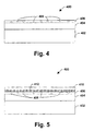
- a layer of high-k dielectric material 404 is formed across the substrate 402 (Fig. 4).
- the substrate 402 generally comprises silicon, while the layer of high-k dielectric material 404 can include any of a number of suitable materials that, alone or in combination, have a dielectric constant (k) greater than that of silicon dioxide (SiO 2 ) or about 3.9.
- Such high-k materials can include, for example, silicon nitride (SiN 4 ), tantalum pentoxide (Ta 2 O 5 ), titanium oxide (TiO 2 ), barium strontium titanate (BST), which have dielectric constants of between 7 and 9, between 20 and 26, 30 and >200, respectively, as well as Al 2 O 3 , ZrO 2 , HfO 2 , zirconium oxynitride, hafnium oxynitride, zirconium silicate, hafnium silicate, zirconium silicon oxynitride, hafnium silicon oxynitride or other suitable materials.
- the layer of high-k dielectric material 404 can be formed across the substrate 402 in any of a number of suitable manners, including, for example, with spin-on techniques, sputtering techniques (e.g., magnetron or ion beam sputtering), growth and/or deposition techniques, such as chemical vapor deposition (CVD).
- spin-on techniques e.g., spin-on or sputtering
- sputtering techniques e.g., magnetron or ion beam sputtering
- growth and/or deposition techniques such as chemical vapor deposition (CVD).
- a top surface 406 (depicted in phantom) of the layer of high-k dielectric material 404 has a plurality electrically active defects 408 (also depicted in phantom) associated therewith.
- a layer of solid material 410 is then formed over the layer of high-k dielectric material 404 (Fig. 5).
- the layer of solid material 406 can be formed across the layer of high-k dielectric material 404 in any suitable manner, such as by growth, deposition and/or spin-on techniques, for example.
- the layer of solid material 406 can comprise, for example, at least one of phosphate silicate glass (PSG) and phosphorous (P) implanted SiO 2 , and includes at least some type of dopant material 412 (depicted as a shading therein).
- the layer of solid material can also have, for example, a thickness of between about 50 to 1000 Angstroms.
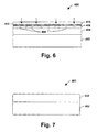
- At least some of the dopant material 412 is then driven into the top surface 406 of the layer of high-k dielectric material 404 to passivate at least some of the electrically active defects 408 located within the top surface 406 of the layer of high-k dielectric material 404 (Fig. 6).
- the layer of solid material 410 can, for example, be heated to a temperature of about 250 to 1000 degrees C for about 1 second to 1 hour to facilitate driving the dopant into the layer of high-k dielectric material 404.
- At least some of the properties of the dopant 412 cause it to be attracted to the electrically active defects 408 and to neutralize at least some of the defects 408.
- the layer of solid material 410 can also be comprised of at least one of boron oxide (B 2 O 3 ) and P 2 O 5 , can have a thickness of between about 50 to 1000 Angstroms and can be heated to a temperature of about 250 to 650 degrees C for about 20 to 40 minutes, for example, to drive the dopant 412 into the layer of high-k dielectric material 404 and passivate the electrically active defects 408.
- B 2 O 3 boron oxide
- P 2 O 5 can have a thickness of between about 50 to 1000 Angstroms and can be heated to a temperature of about 250 to 650 degrees C for about 20 to 40 minutes, for example, to drive the dopant 412 into the layer of high-k dielectric material 404 and passivate the electrically active defects 408.
- the electrically active defects 408 can be passivated by subjecting the layer of high-k dielectric material 404 to a gas phase treatment with annealing.
- the substrate and layer of high-k dielectric material can be placed into a chamber, such as a furnace, for example, and exposed to a mixture of one or more substances in gaseous form that contain one or more suitable dopants, such as phosphine PH 3 or arsine AsH 3 , for example.
- the temperature within the chamber can then be adjusted up or down while optionally controlling the pressure within the chamber to cause the dopants from the gaseous phase to react with and neutralize the electrically active defects 408 located within the top surface 406 of the layer of high-k dielectric material 404.
- Byproducts of the reaction such as residual solids, can then be removed from the layer of high-k dielectric material 404, such as by chemical mechanical polishing (CMP), dry etch, wet etch, or de-ionized water rinse, for example.
- CMP chemical mechanical polishing
- the layer of solid material 410 is stripped away after being heated.
- the layer of solid material 410 can be removed in any suitable manner, such as by acid rinsing, for example, to expose the substantially defect free layer of high-k dielectric material 404 (Fig. 7).
- a gate electrode layer 414 is then formed over the layer of high-k dielectric material 404 ( e.g. , via spin -on, sputtering, deposition, growth techniques, etc.) (Fig. 8).
- the gate electrode layer 414 generally comprises polysilicon or an equivalent, and is patterned in any suitable manner, via etching, for example, to form a gate electrode structure or gate contact 416 of the transistor 400 (Fig. 9).
- the contact 416 provides a means for applying a voltage to the transistor 400 or otherwise biasing the transistor 400.
- the substantially defect free layer of high-k dielectric material 404 can also be patterned ( e . g ., via etching) to produce a gate dielectric 418 between the gate electrode 416 and the substrate 402 (Fig. 10).
- the gate dielectric 418 and gate electrode 416 constitute a gate structure 420 within the transistor 400.
- N or p type dopant 422 is then applied to the substrate 402 on either side of the gate structure 420 to form desired extension regions 424, 426, which are precursors to source and drain regions in the transistor (Fig. 11). It will be appreciated that n-type dopant is applied to form an NMOS transistor, while p-type dopant is applied to form a PMOS transistor. It will be further appreciated that the gate electrode 416 may also receive dopant 422 when the extension regions 424, 426 are created.
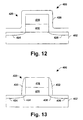
- a layer of an insulating material 428 (e.g., silicon nitride, silicon oxide) is then formed over the entire structure (Fig. 12).
- the layer of insulating material is selectively removed ( e . g ., via anisotropic etching) to form sidewall spacers 430, 432 on either side of the gate structure 420 (Fig. 13).
- the sidewall spacers 430, 432 cover portions 434, 436 of the extension regions 424, 426 and deter subsequently applied dopant from entering these regions 434, 436.
- Additional n or p type dopant 422 is then applied (Fig. 14) to establish source and drain regions 438, 440 within the substrate 402 on either side of the gate structure 420 (Fig. 15).
- the additional dopant 422 is of substantially the same type as that previously applied in forming the extension regions 424, 426 ( e.g. , Fig. 11).
- a channel region 442 is thereby defined within the substrate 402 under the gate structure 420 as the source and drain regions 438, 440 are formed.
- the gate electrode 418 may also receive dopant 422 when the source and drain regions 438, 440 are formed, which doping will have minimal exposure to the adverse effects of electrically active defects present within a top surface of the high-k dielectric since such defects have been passivated.
- the dopant 412 (Figs. 5 and 6) in the donor layer of solid material 410 is likely opposite to the type of dopant 422 that is applied to create the source and drain regions 438, 440. As such, it may be said that the top portion of the high-k dielectric layer is "counter-doped" when the source and drain regions are created.
- the layer of solid material 410 likely includes a p-type dopant (e.g. , boron). As such, when the source and drain regions are created the transistor 400 is "counter-doped" with a n-type dopant 422.
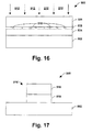
- Fig. 16 illustrates a cross-sectional view of the makings of a transistor 500 formed upon a substrate 502 where a layer of high-k dielectric material 504 is formed across the substrate 502 and a gate electrode layer 506 (e.g. , polysilicon) is formed across the layer of high-k dielectric material 504.
- a top portion 508 (depicted in phantom) of the layer of high-k dielectric material 504 comprises a plurality of electrically active defects 510.
- a dopant 512 can be implanted into the gate electrode layer 506 and annealed to diffuse therethrough and passivate the electrically active defects 510.
- the gate electrode layer 506 and the now neutralized layer of high-k dielectric material 504 can then be patterned (e.g., via etching) to establish a gate structure 514 upon the substrate 504 (Fig. 17).
- the gate structure 514 includes a gate electrode 516 and a gate dielectric 518 that electrically insulates the gate electrode 516 from the substrate 502.
- the transistor can then be lightly "counter-doped" with n or p type dopant 520 (Fig. 18) to form extension regions 522, 524 within the substrate 502 on opposite sides of the gate structure 514 (Fig. 19). It will be appreciated that the gate electrode 516 can also receive some of the dopant 520 during this doping process.
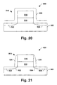
- a layer of an insulating material 526 (e.g., silicon nitride, silicon oxide) can then be formed over the entire structure (Fig. 20).
- the layer of insulating material is selectively removed ( e.g. , via anisotropic etching) to form sidewall spacers 528, 530 on either side of the gate structure 514 (Fig. 21).
- the sidewall spacers 528, 530 cover portions 532, 534 of the extension regions 522, 524 and deter subsequently applied dopant from entering these regions 532, 534.
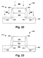
- Additional n or p type dopant 520 is then applied (Fig. 22) to establish source and drain regions 536, 538 within the substrate 502 on either side of the gate structure 514 (Fig. 23).
- the additional dopant 520 (Fig. 22) is of substantially the same type as that previously applied in forming the extension regions 522, 524 ( e.g. , Figs. 18, 19).
- a channel region 540 is defined within the substrate 502 under the gate structure 514 as the source and drain regions 536, 538 are formed (Fig. 23).
- the gate electrode 516 may also receive dopant 520 when the source and drain regions 536, 538 are formed, which doping will have minimal exposure to the adverse effects of electrically active defects present within a top surface of the high-k dielectric since such defects have been passivated.
- the polysilicon layer 506 can be doped prior to patterning with a p-type dopant, wherein the p-type dopant diffuses down to the poly/high-k interface and passivates electrically active defects 510 associated thereat (region 508, Fig. 16). Then, after patterning the polysilicon, an n-type implant is performed which forms the n-type source/drain regions while concurrently counterdoping the poly gate 516. Furthermore, n-type dopant from the poly gate 516 may combine with the p-type dopant at region 508 to render that region generally neutral thereat, and thus mitigate any potential impact.
- one or more aspects of the present invention provide a methodology for passivating electrically active defects at the interface of a gate electrode and gate dielectric layer.
- Electrically active defects at the interface can severely degrade the channel mobility of transistor devices either by trapping and releasing electrons, or by providing a charged site that would apply a force normal to current flow. Either of these effects will inhibit current flow and subsequently reduce the channel mobility as well as severly degrade V fb and Vt performance.
- Passivating makes the surface of the gate dielectric less reactive with the polysilicon gate and neutralizes the reactivity of that surface with the polysilicon. Consequently, resulting semiconductor devices are more reliable, are more uniform with regard to their performance characteristics and can be produced with a higher effective yield.
Landscapes
- Insulated Gate Type Field-Effect Transistor (AREA)
- Metal-Oxide And Bipolar Metal-Oxide Semiconductor Integrated Circuits (AREA)
- Formation Of Insulating Films (AREA)
Abstract
Description
Claims (10)
- A method of forming a transistor comprising:forming a high-k dielectric layer over a semiconductor substrate, the high-k dielectric layer having a top surface associated therewith;passivating electrically active defects associated with the top surface of the high-k dielectric layer;forming a gate electrode layer over the high-k dielectric layer;patterning the gate electrode layer to form a gate electrode structure; andforming source and drain regions in the semiconductor substrate on opposite sides of the gate electrode structure, and defining a channel region therebetween.
- The method of claim 1, wherein passivating the electrically active defects comprises:forming a donor layer having a dopant associated therewith over the high-k dielectric layer;driving the dopant from the donor layer into the high-k dielectric layer, wherein the dopant neutralizes at least some of the electrically active defects.
- The method claim 2, wherein driving the dopant into the high-k layer comprises:heating the donor layer to a temperature of about 250 to 1000 degrees C for about 1 second to 1 hour.
- The method of claim 3, wherein the donor layer comprises at least one of phospho-silicate glass (PSG), borosilicate glass (BSG), borophosphosilicate glass (BPSG), phosphorous (P) implanted SiO2, boron (B) implanted into SiO2, boric oxide (B2O3) and phosphoric oxide (P2O5).
- The method of any one of claims 2 to 4, wherein the donor layer comprises a thickness of between about 50 to 1000 Angstroms.
- The method of any one of claims 2 to 5, further comprising:removing the donor layer after passivating the electrically active defects.
- The method of claim 1, wherein passivating the electrically active defects comprises:exposing the top surface of the high-k dielectric layer to gaseous forms of a p-type or n-type dopant; andannealing the high-k dielectric layer such that at least some of the dopant gas is attracted to and neutralizes at least some of the electrically active defects.
- The method of claim 7, wherein the dopant gas comprises at least one of phosphine (PH3) and arsine (AsH3).
- The method of claim 1, wherein the gate electrode layer is formed over the high-k dielectric layer prior to passivating the electrically active defects, the method comprising:doping the gate electrode layer; andannealing the gate electrode layer such that at least some of the dopant is attracted to at least some of the electrically active defects to neutralize at least some of the electrically active defects.
- The method of claim 9, wherein doping the gate electrode comprises doping the gate electrode with a p-type dopant for an NMOS transistor or an n-type dopant for a PMOS transistor before patterning the gate electrode, and wherein forming the source and drain regions comprises doping the substrate and the gate electrode after a patterning thereof with an n-type dopant for the NMOS transistor or a p-type dopant for the PMOS transistor.
Applications Claiming Priority (2)
| Application Number | Priority Date | Filing Date | Title |
|---|---|---|---|
| US10/335,560 US7015088B2 (en) | 2002-12-31 | 2002-12-31 | High-K gate dielectric defect gettering using dopants |
| US335560 | 2002-12-31 |
Publications (2)
| Publication Number | Publication Date |
|---|---|
| EP1435650A2 true EP1435650A2 (en) | 2004-07-07 |
| EP1435650A3 EP1435650A3 (en) | 2008-09-03 |
Family
ID=32507395
Family Applications (1)
| Application Number | Title | Priority Date | Filing Date |
|---|---|---|---|
| EP03104980A Withdrawn EP1435650A3 (en) | 2002-12-31 | 2003-12-24 | Method of forming a transistor |
Country Status (3)
| Country | Link |
|---|---|
| US (1) | US7015088B2 (en) |
| EP (1) | EP1435650A3 (en) |
| JP (1) | JP2004214662A (en) |
Families Citing this family (6)
| Publication number | Priority date | Publication date | Assignee | Title |
|---|---|---|---|---|
| JPWO2007091302A1 (en) * | 2006-02-07 | 2009-06-25 | 富士通マイクロエレクトロニクス株式会社 | Semiconductor device and manufacturing method thereof |
| US7407871B2 (en) * | 2006-09-05 | 2008-08-05 | Tech Semiconductor Singapore Pte Ltd | Method for passivation of plasma etch defects in DRAM devices |
| KR101044692B1 (en) | 2008-08-07 | 2011-06-28 | 주식회사 하이닉스반도체 | How to Form a Flash Memory Device |
| US9478616B2 (en) | 2011-03-03 | 2016-10-25 | Cree, Inc. | Semiconductor device having high performance channel |
| US8658490B2 (en) * | 2012-04-04 | 2014-02-25 | Globalfoundries Inc. | Passivating point defects in high-K gate dielectric layers during gate stack formation |
| US10629749B2 (en) * | 2017-11-30 | 2020-04-21 | Taiwan Semiconductor Manufacturing Co., Ltd. | Method of treating interfacial layer on silicon germanium |
Family Cites Families (11)
| Publication number | Priority date | Publication date | Assignee | Title |
|---|---|---|---|---|
| US6320238B1 (en) * | 1996-12-23 | 2001-11-20 | Agere Systems Guardian Corp. | Gate structure for integrated circuit fabrication |
| US5861335A (en) * | 1997-03-21 | 1999-01-19 | Advanced Micro Devices, Inc. | Semiconductor fabrication employing a post-implant anneal within a low temperature high pressure nitrogen ambient to improve channel and gate oxide reliability |
| US6396092B1 (en) * | 1997-03-27 | 2002-05-28 | Hitachi, Ltd. | Semiconductor device and method for manufacturing the same |
| US6117739A (en) * | 1998-10-02 | 2000-09-12 | Advanced Micro Devices, Inc. | Semiconductor device with layered doped regions and methods of manufacture |
| US6051865A (en) * | 1998-11-09 | 2000-04-18 | Advanced Micro Devices, Inc. | Transistor having a barrier layer below a high permittivity gate dielectric |
| US6303520B1 (en) * | 1998-12-15 | 2001-10-16 | Mattson Technology, Inc. | Silicon oxynitride film |
| US6297539B1 (en) * | 1999-07-19 | 2001-10-02 | Sharp Laboratories Of America, Inc. | Doped zirconia, or zirconia-like, dielectric film transistor structure and deposition method for same |
| US6638877B2 (en) * | 2000-11-03 | 2003-10-28 | Texas Instruments Incorporated | Ultra-thin SiO2using N2O as the oxidant |
| US6844604B2 (en) * | 2001-02-02 | 2005-01-18 | Samsung Electronics Co., Ltd. | Dielectric layer for semiconductor device and method of manufacturing the same |
| US6369430B1 (en) * | 2001-04-02 | 2002-04-09 | Motorola, Inc. | Method of preventing two neighboring contacts from a short-circuit caused by a void between them and device having the same |
| US6642131B2 (en) * | 2001-06-21 | 2003-11-04 | Matsushita Electric Industrial Co., Ltd. | Method of forming a silicon-containing metal-oxide gate dielectric by depositing a high dielectric constant film on a silicon substrate and diffusing silicon from the substrate into the high dielectric constant film |
-
2002
- 2002-12-31 US US10/335,560 patent/US7015088B2/en not_active Expired - Lifetime
-
2003
- 2003-12-24 EP EP03104980A patent/EP1435650A3/en not_active Withdrawn
- 2003-12-25 JP JP2003430016A patent/JP2004214662A/en not_active Abandoned
Also Published As
| Publication number | Publication date |
|---|---|
| EP1435650A3 (en) | 2008-09-03 |
| US20040127000A1 (en) | 2004-07-01 |
| JP2004214662A (en) | 2004-07-29 |
| US7015088B2 (en) | 2006-03-21 |
Similar Documents
| Publication | Publication Date | Title |
|---|---|---|
| US6426279B1 (en) | Epitaxial delta doping for retrograde channel profile | |
| US6104063A (en) | Multiple spacer formation/removal technique for forming a graded junction | |
| US6894357B2 (en) | Gate stack for high performance sub-micron CMOS devices | |
| US8390080B2 (en) | Transistor with dopant-bearing metal in source and drain | |
| US6410938B1 (en) | Semiconductor-on-insulator device with nitrided buried oxide and method of fabricating | |
| US5846857A (en) | CMOS processing employing removable sidewall spacers for independently optimized N- and P-channel transistor performance | |
| US6060345A (en) | Method of making NMOS and PMOS devices with reduced masking steps | |
| US6660657B1 (en) | Methods of incorporating nitrogen into silicon-oxide-containing layers | |
| US20050202659A1 (en) | Ion implantation of high-k materials in semiconductor devices | |
| US5478763A (en) | High performance field effect transistor and method of manufacture thereof | |
| US6051487A (en) | Semiconductor device fabrication using a sacrificial plug for defining a region for a gate electrode | |
| US5943565A (en) | CMOS processing employing separate spacers for independently optimized transistor performance | |
| US6100204A (en) | Method of making ultra thin gate oxide using aluminum oxide | |
| US7112497B2 (en) | Multi-layer reducible sidewall process | |
| JPH04253341A (en) | Manufacture of transistor | |
| US6207482B1 (en) | Integration method for deep sub-micron dual gate transistor design | |
| US6261885B1 (en) | Method for forming integrated circuit gate conductors from dual layers of polysilicon | |
| US7419867B2 (en) | CMOS gate structure comprising predoped semiconductor gate material with improved uniformity of dopant distribution and method of forming the structure | |
| US8395221B2 (en) | Depletion-free MOS using atomic-layer doping | |
| US7015088B2 (en) | High-K gate dielectric defect gettering using dopants | |
| US7148096B2 (en) | Method of manufacturing a semiconductor device having a gate electrode containing polycrystalline silicon-germanium | |
| US6406952B2 (en) | Process for device fabrication | |
| US7033897B2 (en) | Encapsulated spacer with low dielectric constant material to reduce the parasitic capacitance between gate and drain in CMOS technology | |
| US6110788A (en) | Surface channel MOS transistors, methods for making the same, and semiconductor devices containing the same | |
| US20050136580A1 (en) | Hydrogen free formation of gate electrodes |
Legal Events
| Date | Code | Title | Description |
|---|---|---|---|
| PUAI | Public reference made under article 153(3) epc to a published international application that has entered the european phase |
Free format text: ORIGINAL CODE: 0009012 |
|
| AK | Designated contracting states |
Kind code of ref document: A2 Designated state(s): AT BE BG CH CY CZ DE DK EE ES FI FR GB GR HU IE IT LI LU MC NL PT RO SE SI SK TR |
|
| AX | Request for extension of the european patent |
Extension state: AL LT LV MK |
|
| RIN1 | Information on inventor provided before grant (corrected) |
Inventor name: ROTONDARO, ANTONIO L P Inventor name: CHAMBERS, JAMES J. Inventor name: COLOMBO, LUIGI |
|
| PUAL | Search report despatched |
Free format text: ORIGINAL CODE: 0009013 |
|
| AK | Designated contracting states |
Kind code of ref document: A3 Designated state(s): AT BE BG CH CY CZ DE DK EE ES FI FR GB GR HU IE IT LI LU MC NL PT RO SE SI SK TR |
|
| AX | Request for extension of the european patent |
Extension state: AL LT LV MK |
|
| AKX | Designation fees paid | ||
| REG | Reference to a national code |
Ref country code: DE Ref legal event code: 8566 |
|
| STAA | Information on the status of an ep patent application or granted ep patent |
Free format text: STATUS: THE APPLICATION IS DEEMED TO BE WITHDRAWN |
|
| 18D | Application deemed to be withdrawn |
Effective date: 20090304 |