EP1435623A1 - Stabilisation method of the drain voltage in non-volatile multilevel memory cells and relating memory device - Google Patents
Stabilisation method of the drain voltage in non-volatile multilevel memory cells and relating memory device Download PDFInfo
- Publication number
- EP1435623A1 EP1435623A1 EP02425801A EP02425801A EP1435623A1 EP 1435623 A1 EP1435623 A1 EP 1435623A1 EP 02425801 A EP02425801 A EP 02425801A EP 02425801 A EP02425801 A EP 02425801A EP 1435623 A1 EP1435623 A1 EP 1435623A1
- Authority
- EP
- European Patent Office
- Prior art keywords
- voltage
- regulator
- node
- input
- drain
- Prior art date
- Legal status (The legal status is an assumption and is not a legal conclusion. Google has not performed a legal analysis and makes no representation as to the accuracy of the status listed.)
- Granted
Links
Images


Classifications
-
- G—PHYSICS
- G11—INFORMATION STORAGE
- G11C—STATIC STORES
- G11C16/00—Erasable programmable read-only memories
- G11C16/02—Erasable programmable read-only memories electrically programmable
- G11C16/06—Auxiliary circuits, e.g. for writing into memory
- G11C16/10—Programming or data input circuits
- G11C16/12—Programming voltage switching circuits
-
- G—PHYSICS
- G11—INFORMATION STORAGE
- G11C—STATIC STORES
- G11C11/00—Digital stores characterised by the use of particular electric or magnetic storage elements; Storage elements therefor
- G11C11/56—Digital stores characterised by the use of particular electric or magnetic storage elements; Storage elements therefor using storage elements with more than two stable states represented by steps, e.g. of voltage, current, phase, frequency
- G11C11/5621—Digital stores characterised by the use of particular electric or magnetic storage elements; Storage elements therefor using storage elements with more than two stable states represented by steps, e.g. of voltage, current, phase, frequency using charge storage in a floating gate
- G11C11/5628—Programming or writing circuits; Data input circuits
Definitions
- the present invention relates to a stabilisation method of the drain voltage in non volatile multilevel memory cells.
- the invention relates also to a memory electronic device arranged to implement said method.
- the invention relates to a multilevel non volatile memory electronic device monolithically integrated on a semiconductor and comprising a programming circuit associated to a matrix of nonvolatile memory cells each one being equipped with at lest a floating gate transistor with corresponding source, drain and gate terminals, each programming circuit incorporating a drain voltage regulator having an output connected to the cell drain terminals in a common circuit node and through a metal line conduction path having a parasitic intrinsic resistance.
- the invention relates to a method for stabilising the voltage at both ends of a load among a plurality of loads associated to a supply line and active one at a time, of the type wherein the application of said voltage is provided through a voltage regulator having an output connected to the loads by means of said supply line and a plurality of routing resistances, each one being associated to a corresponding load.
- the node stability becomes an even more critical problem.
- the attached figure 1 shows the distributions of the four different programming states of this cell, that is the distributions of its possible threshold voltage values.
- the programming step of a Flash cell is always preceded by an erasing step; consequently, in the beginning the cell is brought to the state "11", the state with the lowest threshold.
- the programming algorithm can be split into n almost identical steps.
- the Flash memory cell is biased keeping the Drain node at a fixed voltage value (typically +4V), the Source node to ground and the Body at a fixed negative value (typically -1,2V).
- the Gate node is initially set at a voltage of 1,5V, to be then increased in following steps (for example) by 300mV at each further step. This leads to an increase by steps in the cell threshold voltage, as shown in figure 1.
- the state of the cell is tested through a reading operation (verify); if the cell does not reach the desired distribution, the operation is repeated by increasing the gate voltage. If, on the contrary, the cell threshold voltage reaches the desired distribution, the programming ends.
- the programming step does not involve only one cell, but it is applied in parallel to a certain number of cells.
- the desired threshold value i.e. it reaches the desired threshold distribution
- they are "excluded” from the following programming step which continues only for the remaining cells which must still reach the predetermined state.
- the programming step involves in parallel about seventy cells, which are a variable current load for the drain voltage regulator during the different programming steps.
- the changes of the threshold voltage and of the applied gate voltage cause a different current absorption by the memory cells; moreover, when the cells have reached the desired state, they are disconnected through a program load transistor, for example as shown in the electric scheme of figure 2.
- the cell drain voltage regulator in the different programming steps, must provide a constant voltage value, but in different current load conditions.
- VPD (+4V) is derived from the Band Gap reference voltage (VGB) according to the following relation:
- the drain regulator for layout requirements, can be at a certain distance from the program load transistors (PL).
- the interconnection metal line bringing the adjusted voltage VPD to these transistors, inserts a parasitic resistance, quantifiable in some tens of ohms. Considering that each memory cell can absorb a drain current of about 60 ⁇ A, with seventy cells being programmed the total current can reach 4mA.
- the cells whereon the programming step continues can have a drain voltage being changed by exactly + 100mV, in the borderline case.
- FIG. 4 Some typical curves showing the threshold voltage change in the programming step according to different drain voltage values are schematically represented in figure 4.
- the diagram of figure 4 indicates in the abscissa the gate voltage and in the ordinate the threshold voltage.
- the cell threshold voltage change follows one of these characteristics. If, on the contrary, the drain voltage changes in programming, the threshold voltage change translates on another characteristic.
- the technical problem underlying the present invention is to provide a method for stabilising the drain voltage and a corresponding non volatile memory device having respective functional and structural characteristics as to improve the Flash cell drain voltage stability, avoiding however the use of voltage regulators positioned near the cell drains. Based on the above, the drain voltage is influenced by the change in the current absorption during the different programming steps.
- the solution idea underlying the present invention is to draw the feedback potential of the voltage regulator in correspondence with the Program Load transistors and no more at the regulator output, making therefore the voltage on the load node independent from the parasitic resistance on the metal line and from the variable current load.
- circuit portion 1 of a memory electronic device according to the present invention is globally and schematically indicated with 1.
- the circuit portion 1 is structured to locally regulate voltage values on the drain terminals of multilevel non volatile memory cells 3 during the programming step thereof. More particularly, the circuit portion 1 refers to a drain regulator 2 connected to a load circuit node A by means of a metal line 4.
- the memory matrix columns i.e. the drain terminals of memory cells 3, belong to the circuit node A, with starting interposition of a program load transistor PL.
- Memory device means any monolithic electronic system incorporating an matrix of memory cells, organised in rows and columns, as well as circuit portions associated to the cell matrix and responsible for the addressing, decoding, reading, writing and erasing of the memory cell content.
- Such a device can be for example a semiconductor-integrated memory chip and of the non volatile EEPROM Flash type split in sectors and electrically erasable.
- Each multilevel memory cell comprises a floating gate transistor with source S, drain D and control gate G terminals.
- each circuit being supplied by a specific supply voltage generated inside the integrated memory circuit and regulated by means of said drain voltage regulator 2.
- a first solution example according to the invention provides that the drain voltage regulator 2, output-connected to the node A by means of the metal line 4, has an input feedback-connected to the same node A.
- a first resistance Rf, of gain, and a second resistance R parf representing the parasitic resistance of the feedback metal line 5 are indicated on the feedback path 5
- the series of resistances RF and R parf is thus a resistive value which can be assigned to this feedback connection.
- the regulator 2 input interested in the feedback is the inverting input (-); the other input is kept at a stable voltage reference, for example a bandgap voltage Vbg.
- This configuration makes the node A voltage independent from the parasitic resistance R pars value and thus from the variable current load.
- the feedback node is no more drawn as in the prior art at the regulator 2 output, but near the program load transistors PL.
- the interconnection parasitic resistance R pars is thus incorporated inside the feedback loop.
- this expedient allows a voltage value regulated to 4V to be kept on said node A.
- the voltage is regulated to 4V at the voltage regulator 2 output, but on the load node A.
- the node OUT is thus regulated by the feedback to obtain 4V on the node A.
- Rparf is the parasitic resistance of the feedback metal line 5 equal to some hundreds of ohms, and it can be also ignored if Rf is high enough.
- This parasitic resistance Rparf once estimated, does not cause voltage changes in node A since the load current does not flow in this resistance.
- a unitary gain buffer 7, for example of the Voltage Follower type, is provided to be inserted immediately downstream of the drain voltage regulator 2.
- the feedback node A is drawn once again downstream of the resistance R pars and not at the regulator 2 output.
- This configuration keeps the voltage upstream of the Program Load transistors exactly equal to the voltage VPD at inputting buffer 7, and the gain (unitary) of the latter is not influenced by the resistance R parf .
- Figures 7A and 7B show the detailed electric schemes of a known solution, for example the solution schematised in figure 2, and of the solution according to the invention, for example the solution schematised in figure 5.
- the method and device according to the invention are particularly effective in all those situations requiring a plurality of loads belonging to a same resistive line, not necessarily memory cells connected to a same metal line, to be supplied with constant regulated voltages.
- line 4 is a supply line which, starting from the regulation 2 output, distributes the voltage to the loads by means of said routing resistances Rpars0, Rpars1, ..., RparsN associated to each load.
- the node indicated with F near the farthest load from the regulator is the node to be used for the feedback connection 5 of the regulator 2.
- the inverting input of the regulator 2 has a high impedance since it is generally formed by means of the gate terminal of a MOS transistor.
- the voltage supplied to each single load is stable against changes in the load being from time to time operative.
- the method and the programming circuit according to the invention solve the technical problem and allow the voltages at the drain memory cell terminals to be stabilised during the multilevel Flash memory programming steps.
Landscapes
- Engineering & Computer Science (AREA)
- Computer Hardware Design (AREA)
- Read Only Memory (AREA)
- Non-Volatile Memory (AREA)
- Semiconductor Memories (AREA)
Abstract
Description
- The present invention relates to a stabilisation method of the drain voltage in non volatile multilevel memory cells.
- The invention relates also to a memory electronic device arranged to implement said method.
- More particularly, the invention relates to a multilevel non volatile memory electronic device monolithically integrated on a semiconductor and comprising a programming circuit associated to a matrix of nonvolatile memory cells each one being equipped with at lest a floating gate transistor with corresponding source, drain and gate terminals, each programming circuit incorporating a drain voltage regulator having an output connected to the cell drain terminals in a common circuit node and through a metal line conduction path having a parasitic intrinsic resistance.
- Even more generally, the invention relates to a method for stabilising the voltage at both ends of a load among a plurality of loads associated to a supply line and active one at a time, of the type wherein the application of said voltage is provided through a voltage regulator having an output connected to the loads by means of said supply line and a plurality of routing resistances, each one being associated to a corresponding load.
- As it is well known in this specific technical field, during the programming step of a Flash memory cell, it is important to set the voltage applied to its terminals (Gate Source Drain and Body).
- In the multilevel flash memory field, wherein the cell is programmed at different threshold voltage values, the node stability becomes an even more critical problem.
- The simple case of programming a multilevel cell with two bits per cell will be considered first, i.e. a two-level cell with four possible combinations of storable logic values.
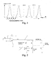
- The attached figure 1 shows the distributions of the four different programming states of this cell, that is the distributions of its possible threshold voltage values.
- The programming step of a Flash cell is always preceded by an erasing step; consequently, in the beginning the cell is brought to the state "11", the state with the lowest threshold.
- The programming algorithm can be split into n almost identical steps. In the first part of each of these steps the Flash memory cell is biased keeping the Drain node at a fixed voltage value (typically +4V), the Source node to ground and the Body at a fixed negative value (typically -1,2V).
- The Gate node is initially set at a voltage of 1,5V, to be then increased in following steps (for example) by 300mV at each further step. This leads to an increase by steps in the cell threshold voltage, as shown in figure 1.
- In the second part of each single programming step the state of the cell is tested through a reading operation (verify); if the cell does not reach the desired distribution, the operation is repeated by increasing the gate voltage. If, on the contrary, the cell threshold voltage reaches the desired distribution, the programming ends.
- In fact the programming step does not involve only one cell, but it is applied in parallel to a certain number of cells. When one or more cells reach the desired threshold value (i.e. it reaches the desired threshold distribution), they are "excluded" from the following programming step which continues only for the remaining cells which must still reach the predetermined state.
- In memory devices of more recent production the programming step involves in parallel about seventy cells, which are a variable current load for the drain voltage regulator during the different programming steps.
- In fact, the changes of the threshold voltage and of the applied gate voltage cause a different current absorption by the memory cells; moreover, when the cells have reached the desired state, they are disconnected through a program load transistor, for example as shown in the electric scheme of figure 2.
- It can thus be understood that the cell drain voltage regulator, in the different programming steps, must provide a constant voltage value, but in different current load conditions.
- The drain voltage VPD (+4V) is derived from the Band Gap reference voltage (VGB) according to the following relation:

- Which expresses the gain of a fedback voltage amplifier, in a noninverting configuration.
- The drain regulator, for layout requirements, can be at a certain distance from the program load transistors (PL). The interconnection metal line bringing the adjusted voltage VPD to these transistors, inserts a parasitic resistance, quantifiable in some tens of ohms. Considering that each memory cell can absorb a drain current of about 60µA, with seventy cells being programmed the total current can reach 4mA.
- Supposing to have a parasitic resistance Rpars whose metal is equal to 25Ω, as shown in figure 3, the voltage drop on the metals can reach up to 100 mV.
- Since the cells which have reached the convenient distribution are disconnected from the adjusted voltage VPD, the cells whereon the programming step continues can have a drain voltage being changed by exactly + 100mV, in the borderline case.
- Some typical curves showing the threshold voltage change in the programming step according to different drain voltage values are schematically represented in figure 4. The diagram of figure 4 indicates in the abscissa the gate voltage and in the ordinate the threshold voltage.
- If the drain voltage is constant during all the programming steps, the cell threshold voltage change follows one of these characteristics. If, on the contrary, the drain voltage changes in programming, the threshold voltage change translates on another characteristic.
- This results in a higher threshold jump and in a widening of the distributions of figure 1 with a corresponding decrease in the reading noise margin or, in the worst case, in real failures due to an excessive distribution widening.
- The technical problem underlying the present invention is to provide a method for stabilising the drain voltage and a corresponding non volatile memory device having respective functional and structural characteristics as to improve the Flash cell drain voltage stability, avoiding however the use of voltage regulators positioned near the cell drains. Based on the above, the drain voltage is influenced by the change in the current absorption during the different programming steps.
- The solution idea underlying the present invention is to draw the feedback potential of the voltage regulator in correspondence with the Program Load transistors and no more at the regulator output, making therefore the voltage on the load node independent from the parasitic resistance on the metal line and from the variable current load.
- On the basis of this solution idea the technical problem is solved by a method as previously described and defined in the characterising part of
claims - The technical problem is solved also by a memory electronic device as defined in the characterising part of
claim 7. - The features and advantages of the method and device according to the invention will be apparent from the following description of an embodiment thereof given by way of non-limiting example with reference to the attached drawings.
-
- Figure 1 schematically shows a comparative diagram between the threshold voltage distribution in a conventional two-level memory cell with two bits per cell;
- Figure 2 is a schematic view of a known programming circuit of the program load type;
- Figure 3 shows in a voltage/voltage diagram some curves which are typical of a multilevel memory cell;
- Figure 4 shows the evolutions of the curves which are typical of the threshold voltages according to the drain voltages;
- Figure 5 is a schematic view in principle of a first embodiment of the device according to the invention;
- Figure 6 is a schematic view of a second embodiment of the device according to the invention;
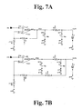
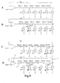
- Figures 7A and 7B are respective schematic views of the circuit layout of a device according to the prior art and according to the present invention;
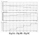
- Figures 8A, 8B and 8C respectively show on diagrams according to time the evolution of voltage signals and current in the device according to the invention compared to a known device;
- Figures 9A, 9B, 9C and 9D are respective schematic views of an example of application of the method according to the invention to a plurality of loads distributed along a resistive line.
-
- With reference to the figures, and particularly to the examples of figures 5 and 6, a
circuit portion 1 of a memory electronic device according to the present invention is globally and schematically indicated with 1. - The
circuit portion 1 is structured to locally regulate voltage values on the drain terminals of multilevel nonvolatile memory cells 3 during the programming step thereof. More particularly, thecircuit portion 1 refers to adrain regulator 2 connected to a load circuit node A by means of ametal line 4. - The memory matrix columns, i.e. the drain terminals of
memory cells 3, belong to the circuit node A, with starting interposition of a program load transistor PL. - Memory device means any monolithic electronic system incorporating an matrix of memory cells, organised in rows and columns, as well as circuit portions associated to the cell matrix and responsible for the addressing, decoding, reading, writing and erasing of the memory cell content.
- Such a device can be for example a semiconductor-integrated memory chip and of the non volatile EEPROM Flash type split in sectors and electrically erasable.
- Each multilevel memory cell comprises a floating gate transistor with source S, drain D and control gate G terminals.
- Among the circuit portions associated to the cell matrix programming circuits are provided, each circuit being supplied by a specific supply voltage generated inside the integrated memory circuit and regulated by means of said
drain voltage regulator 2. - In accordance with the present invention, it has been provided to feedback-connect said node A to an input of the
regulator 2. The parasitic resistance Rpars on the metal line is therefore substantially incorporated in the feedback loop. - A first solution example according to the invention provides that the
drain voltage regulator 2, output-connected to the node A by means of themetal line 4, has an input feedback-connected to the same node A. - A first resistance Rf, of gain, and a second resistance Rparf representing the parasitic resistance of the
feedback metal line 5 are indicated on thefeedback path 5 - The series of resistances RF and Rparf is thus a resistive value which can be assigned to this feedback connection.
- The
regulator 2 input interested in the feedback is the inverting input (-); the other input is kept at a stable voltage reference, for example a bandgap voltage Vbg. - This configuration makes the node A voltage independent from the parasitic resistance Rpars value and thus from the variable current load.
- Therefore, advantageously, the feedback node is no more drawn as in the prior art at the
regulator 2 output, but near the program load transistors PL. The interconnection parasitic resistance Rpars is thus incorporated inside the feedback loop. - Moreover, since at the amplifier inverting input the node OUT is no more fedback, but node A is fedback, this expedient allows a voltage value regulated to 4V to be kept on said node A.
- In fact it does not matter that the voltage is regulated to 4V at the
voltage regulator 2 output, but on the load node A. The node OUT is thus regulated by the feedback to obtain 4V on the node A. - The node OUT will move on the basis of the load current according to the following relation:
- While the voltage on node A satisfies the following formula:
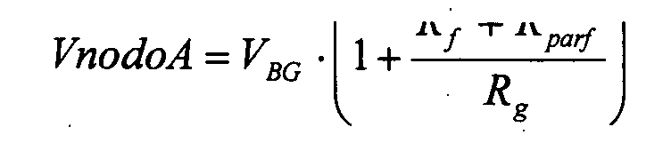
- Where Rparf is the parasitic resistance of the
feedback metal line 5 equal to some hundreds of ohms, and it can be also ignored if Rf is high enough. - This parasitic resistance Rparf, once estimated, does not cause voltage changes in node A since the load current does not flow in this resistance.
- With particular reference to the example of figure 6, an alternative embodiment comprised within the principles of the present invention is now described.
- In this second embodiment a
unitary gain buffer 7, for example of the Voltage Follower type, is provided to be inserted immediately downstream of thedrain voltage regulator 2. - This second solution, though preserving the advantages of the previous solution, has the further advantage of totally eliminating also the parasitic resistance Rparf effect of the
feedback metal line 5. - The feedback node A is drawn once again downstream of the resistance Rpars and not at the
regulator 2 output. - This configuration keeps the voltage upstream of the Program Load transistors exactly equal to the voltage VPD at inputting
buffer 7, and the gain (unitary) of the latter is not influenced by the resistance Rparf. - Figures 7A and 7B show the detailed electric schemes of a known solution, for example the solution schematised in figure 2, and of the solution according to the invention, for example the solution schematised in figure 5.
- With reference to figures 7A and 7B, in figures 8A, 8B and 8C the evolutions of voltage values according to the current load can be compared to each other, with the known solution (short dashes line) and the solution of the invention (continuous line).
- The method and device according to the invention are particularly effective in all those situations requiring a plurality of loads belonging to a same resistive line, not necessarily memory cells connected to a same metal line, to be supplied with constant regulated voltages.
- Let's suppose for example to be in a situation as the one shown in figure 9A, requiring some load sources L0, L1, ..., LN spaced from each other; and thus with different associated routing resistances Rpars0, Rpars1, ..., RparsN, to be supplied with different voltages VREF.
- In this
case line 4 is a supply line which, starting from theregulation 2 output, distributes the voltage to the loads by means of said routing resistances Rpars0, Rpars1, ..., RparsN associated to each load. - The node indicated with F near the farthest load from the regulator is the node to be used for the
feedback connection 5 of theregulator 2. - Let's suppose then that only one load, for example L1, absorbs current, while the others are off or have a void current absorbed. On node A connected to L1 the desired voltage VREF is reached; in fact on the right of node A there is no current absorption since the current generators on the right are off. Moreover, the inverting input of the
regulator 2 has a high impedance since it is generally formed by means of the gate terminal of a MOS transistor. - If the load L1 is now deactivated, and in the meantime another load is enabled, for example L4, the voltage VREF reaches the node to which the load L4 is connected, indicated in figure 9C still with node A.
- In substance, the voltage supplied to each single load is stable against changes in the load being from time to time operative.
- In conclusion, the method and the programming circuit according to the invention solve the technical problem and allow the voltages at the drain memory cell terminals to be stabilised during the multilevel Flash memory programming steps.
- Moreover, the previously shown solution, by acting in order to keep the value of these voltages stable in programming, allows gate pulses applied during the programming algorithm to effectively realise a threshold voltage jump which is constant for each pulse with any kind of programming pattern.
Claims (10)
- A method for stabilising the voltage on the drain terminals of multilevel non volatile memory cells (3) in the programming step, of the type wherein the application of said voltage is provided through a drain voltage regulator (2) having an output (OUT) connected to said terminals in a common circuit node (A) by means of a metal line (4) conduction path having a parasitic intrinsic resistance (Rpars), characterised in that it is provided with a feedback path (5) between said node (A) and an input of the regulator (2).
- A method according to claim 1, characterised in that said feedback path (5) comprises a resistance (Rf) and a parasitic intrinsic resistance (Rparf) having a negligible value.
- A method according to claim 1, characterised in that said input of the regulator (2) is the inverting input (-).
- A method according to claim 1, characterised in that it is provided with a buffer (7) inserted between said output (OUT) of the regulator and said node (A), as well as a feedback path (5) between said node (A) and an input of said buffer (7).
- A method for stabilising the voltage at both ends of a load (Li) among a plurality of loads (L0, L1, ..., Ln) associated to a supply line (4) and active one at a time, of the type in which the application of said voltage is provided by means of a voltage regulator (2) having an output (OUT) connected to the loads through said supply line (4) and a plurality of routing resistances (Rpars0, Rpars1, ..., RparsN,) each one being associated to a corresponding load (L0, L1, ..., Ln), characterised in that it provides a feedback path (5) between one end (F) of the farthest load (Ln) from the regulator (2) and an input of the regulator (2) itself.
- A method according to claim 5, characterised in that said feedback path (5) comprises only a parasitic intrinsic resistance (Rparf) having a negligible value.
- A multilevel non volatile memory electronic device monolithically integrated on a semiconductor and comprising a programming circuit associated to an matrix of non volatile memory cells (3), each one being equipped with at least a floating gate transistor with corresponding source (S), drain (D) and gate (G) terminals, each programming circuit incorporating a drain voltage regulator (2) having an output (OUT) connected to the cell drain terminals (D) in a common circuit node (A) and through a metal line conduction path (4) having a parasitic intrinsic resistance (Rpars), characterised in that it comprises a feedback path (5) between said node (A) and an input of the regulator (2).
- A device according to claim 6, characterised in that said feedback path (5) comprises a resistance (Rf) and a parasitic intrinsic resistance (Rparf) having a negligible value.
- A device according to claim 6, characterised in that said input of the regulator (2) is the inverting input (-).
- A device according to claim 6, characterised in that it provides a buffer (7) inserted between said output (OUT) of the regulator and said node (A), as well as a feedback path (5) between said node (A) and an input of said buffer (7).
Priority Applications (3)
| Application Number | Priority Date | Filing Date | Title |
|---|---|---|---|
| DE60226987T DE60226987D1 (en) | 2002-12-30 | 2002-12-30 | A method for stabilizing the drain voltage in a multi-state nonvolatile memory and associated memory device |
| EP02425801A EP1435623B1 (en) | 2002-12-30 | 2002-12-30 | Stabilisation method of the drain voltage in non-volatile multilevel memory cells and relating memory device |
| US10/748,701 US7031191B2 (en) | 2002-12-30 | 2003-12-30 | Stabilization method for drain voltage in non-volatile multi-level memory cells and related memory device |
Applications Claiming Priority (1)
| Application Number | Priority Date | Filing Date | Title |
|---|---|---|---|
| EP02425801A EP1435623B1 (en) | 2002-12-30 | 2002-12-30 | Stabilisation method of the drain voltage in non-volatile multilevel memory cells and relating memory device |
Publications (2)
| Publication Number | Publication Date |
|---|---|
| EP1435623A1 true EP1435623A1 (en) | 2004-07-07 |
| EP1435623B1 EP1435623B1 (en) | 2008-06-04 |
Family
ID=32479856
Family Applications (1)
| Application Number | Title | Priority Date | Filing Date |
|---|---|---|---|
| EP02425801A Expired - Lifetime EP1435623B1 (en) | 2002-12-30 | 2002-12-30 | Stabilisation method of the drain voltage in non-volatile multilevel memory cells and relating memory device |
Country Status (3)
| Country | Link |
|---|---|
| US (1) | US7031191B2 (en) |
| EP (1) | EP1435623B1 (en) |
| DE (1) | DE60226987D1 (en) |
Families Citing this family (4)
| Publication number | Priority date | Publication date | Assignee | Title |
|---|---|---|---|---|
| US7009887B1 (en) * | 2004-06-03 | 2006-03-07 | Fasl Llc | Method of determining voltage compensation for flash memory devices |
| ES2724115T3 (en) * | 2007-06-29 | 2019-09-06 | Midmark Corp | Graphical user interface for computer-assisted margin marking on dentures |
| KR101292574B1 (en) * | 2007-10-08 | 2013-08-16 | 삼성전자주식회사 | Apparatus and method of multi-bit programming |
| US10366752B2 (en) * | 2016-12-11 | 2019-07-30 | Technion Research & Development Foundation Ltd. | Programming for electronic memories |
Citations (4)
| Publication number | Priority date | Publication date | Assignee | Title |
|---|---|---|---|---|
| US5546042A (en) * | 1994-06-01 | 1996-08-13 | Intel Corporation | High precision voltage regulation circuit for programming multiple bit flash memory |
| EP0905710A1 (en) * | 1997-09-30 | 1999-03-31 | STMicroelectronics S.r.l. | Voltage regulator with voltage drop compensation for a programming circuitry of non-volatile electrically programmable memory cells |
| US6285614B1 (en) * | 1997-11-21 | 2001-09-04 | Stmicroelectronics S.R.L. | Voltage regulator for single feed voltage memory circuits, and flash type memory in particular |
| US20020101762A1 (en) * | 2001-01-29 | 2002-08-01 | Masaru Nawaki | Nonvolatile semiconductor memory device |
Family Cites Families (8)
| Publication number | Priority date | Publication date | Assignee | Title |
|---|---|---|---|---|
| JP3247402B2 (en) * | 1991-07-25 | 2002-01-15 | 株式会社東芝 | Semiconductor device and nonvolatile semiconductor memory device |
| DE69325714T2 (en) * | 1993-12-31 | 2000-03-02 | Stmicroelectronics S.R.L., Agrate Brianza | Voltage regulator for non-volatile semiconductor memory devices |
| US5815435A (en) * | 1995-10-10 | 1998-09-29 | Information Storage Devices, Inc. | Storage cell for analog recording and playback |
| US6040993A (en) * | 1998-02-23 | 2000-03-21 | Macronix International Co., Ltd. | Method for programming an analog/multi-level flash EEPROM |
| KR100376262B1 (en) * | 2000-12-29 | 2003-03-17 | 주식회사 하이닉스반도체 | Regulation circuit for bitline voltage |
| US6456557B1 (en) * | 2001-08-28 | 2002-09-24 | Tower Semiconductor Ltd | Voltage regulator for memory device |
| JP4157285B2 (en) * | 2001-08-31 | 2008-10-01 | 株式会社東芝 | Nonvolatile semiconductor memory |
| JP4184745B2 (en) * | 2002-10-03 | 2008-11-19 | 沖電気工業株式会社 | Semiconductor memory device |
-
2002
- 2002-12-30 EP EP02425801A patent/EP1435623B1/en not_active Expired - Lifetime
- 2002-12-30 DE DE60226987T patent/DE60226987D1/en not_active Expired - Lifetime
-
2003
- 2003-12-30 US US10/748,701 patent/US7031191B2/en not_active Expired - Lifetime
Patent Citations (4)
| Publication number | Priority date | Publication date | Assignee | Title |
|---|---|---|---|---|
| US5546042A (en) * | 1994-06-01 | 1996-08-13 | Intel Corporation | High precision voltage regulation circuit for programming multiple bit flash memory |
| EP0905710A1 (en) * | 1997-09-30 | 1999-03-31 | STMicroelectronics S.r.l. | Voltage regulator with voltage drop compensation for a programming circuitry of non-volatile electrically programmable memory cells |
| US6285614B1 (en) * | 1997-11-21 | 2001-09-04 | Stmicroelectronics S.R.L. | Voltage regulator for single feed voltage memory circuits, and flash type memory in particular |
| US20020101762A1 (en) * | 2001-01-29 | 2002-08-01 | Masaru Nawaki | Nonvolatile semiconductor memory device |
Non-Patent Citations (1)
| Title |
|---|
| U. TIETZE - CH. SCHENK: "Halbleiter-Schaltungstechnik", 1974, SPRINGER-VERLAG, BERLIN, XP002239657 * |
Also Published As
| Publication number | Publication date |
|---|---|
| US7031191B2 (en) | 2006-04-18 |
| EP1435623B1 (en) | 2008-06-04 |
| US20040213047A1 (en) | 2004-10-28 |
| DE60226987D1 (en) | 2008-07-17 |
Similar Documents
| Publication | Publication Date | Title |
|---|---|---|
| KR100427739B1 (en) | Power voltage supplying circuit and semiconductor memory including the same | |
| KR100362700B1 (en) | Voltage regulator circuit built in a semiconductor memory device | |
| US8130026B2 (en) | Booster circuit and voltage supply circuit | |
| US5253201A (en) | Writing control circuit employed in non-volatile semiconductor memory device | |
| US7764563B2 (en) | Adjustable voltage regulator for providing a regulated output voltage | |
| US7656225B2 (en) | Voltage generation circuit and semiconductor memory device including the same | |
| US8004902B2 (en) | Nonvolatile semiconductor memory device | |
| KR101256911B1 (en) | Voltage generation circuit | |
| EP0915407B1 (en) | Temperature correlated voltage generator circuit and corresponding voltage regulator for a single power memory cell, particularly of the FLASH-type | |
| US5905677A (en) | Voltage regulator for non-volatile semiconductor electrically programmable memory devices | |
| US5982677A (en) | Compensated voltage regulator | |
| US6480436B2 (en) | Non-volatile memory with a charge pump with regulated voltage | |
| US6320790B1 (en) | Biasing stage for biasing the drain terminal of a nonvolatile memory cell during the read phase | |
| EP1331644B1 (en) | Regulation method for the source voltage in a nonvolatile memory cell during programming and corresponding program circuit | |
| US7508716B2 (en) | Sense amplifier for low-supply-voltage nonvolatile memory cells | |
| JP6887457B2 (en) | Reference voltage generation circuit and non-volatile semiconductor storage device | |
| EP1435623B1 (en) | Stabilisation method of the drain voltage in non-volatile multilevel memory cells and relating memory device | |
| US6809961B2 (en) | Regulation method for the drain, body and source terminals voltages in a non-volatile memory cell during a program phase and corresponding program circuit | |
| EP1453059B1 (en) | Gate voltage regulation system for a non volatile memory cells and a programming and soft programming phase | |
| US8929168B2 (en) | Sense amplifier voltage regulator | |
| US10515707B2 (en) | Temperature compensation for unselected memory cells and string select switches in NAND flash memory | |
| US20050078499A1 (en) | Nonvolatile semiconductor storage apparatus and readout method | |
| JP7061179B2 (en) | Current-voltage conversion circuit, reference voltage generation circuit and non-volatile semiconductor storage device | |
| CN120051827A (en) | Current bias circuit, memory and memory system | |
| CN121393514A (en) | Reference current generating circuit for tracking word line voltage and nonvolatile memory |
Legal Events
| Date | Code | Title | Description |
|---|---|---|---|
| PUAI | Public reference made under article 153(3) epc to a published international application that has entered the european phase |
Free format text: ORIGINAL CODE: 0009012 |
|
| AK | Designated contracting states |
Kind code of ref document: A1 Designated state(s): AT BE BG CH CY CZ DE DK EE ES FI FR GB GR IE IT LI LU MC NL PT SE SI SK TR |
|
| AX | Request for extension of the european patent |
Extension state: AL LT LV MK RO |
|
| 17P | Request for examination filed |
Effective date: 20050103 |
|
| 17Q | First examination report despatched |
Effective date: 20050208 |
|
| AKX | Designation fees paid |
Designated state(s): DE FR GB IT |
|
| 17Q | First examination report despatched |
Effective date: 20050208 |
|
| GRAP | Despatch of communication of intention to grant a patent |
Free format text: ORIGINAL CODE: EPIDOSNIGR1 |
|
| GRAS | Grant fee paid |
Free format text: ORIGINAL CODE: EPIDOSNIGR3 |
|
| GRAA | (expected) grant |
Free format text: ORIGINAL CODE: 0009210 |
|
| AK | Designated contracting states |
Kind code of ref document: B1 Designated state(s): DE FR GB IT |
|
| REG | Reference to a national code |
Ref country code: GB Ref legal event code: FG4D |
|
| REF | Corresponds to: |
Ref document number: 60226987 Country of ref document: DE Date of ref document: 20080717 Kind code of ref document: P |
|
| PLBE | No opposition filed within time limit |
Free format text: ORIGINAL CODE: 0009261 |
|
| STAA | Information on the status of an ep patent application or granted ep patent |
Free format text: STATUS: NO OPPOSITION FILED WITHIN TIME LIMIT |
|
| 26N | No opposition filed |
Effective date: 20090305 |
|
| PGFP | Annual fee paid to national office [announced via postgrant information from national office to epo] |
Ref country code: GB Payment date: 20081125 Year of fee payment: 7 |
|
| PG25 | Lapsed in a contracting state [announced via postgrant information from national office to epo] |
Ref country code: IT Free format text: LAPSE BECAUSE OF FAILURE TO SUBMIT A TRANSLATION OF THE DESCRIPTION OR TO PAY THE FEE WITHIN THE PRESCRIBED TIME-LIMIT Effective date: 20080604 |
|
| REG | Reference to a national code |
Ref country code: FR Ref legal event code: ST Effective date: 20090831 |
|
| PG25 | Lapsed in a contracting state [announced via postgrant information from national office to epo] |
Ref country code: FR Free format text: LAPSE BECAUSE OF NON-PAYMENT OF DUE FEES Effective date: 20081231 |
|
| GBPC | Gb: european patent ceased through non-payment of renewal fee |
Effective date: 20091230 |
|
| PG25 | Lapsed in a contracting state [announced via postgrant information from national office to epo] |
Ref country code: GB Free format text: LAPSE BECAUSE OF NON-PAYMENT OF DUE FEES Effective date: 20091230 |
|
| REG | Reference to a national code |
Ref country code: DE Ref legal event code: R082 Ref document number: 60226987 Country of ref document: DE Representative=s name: SAMSON & PARTNER, PATENTANWAELTE, DE |
|
| REG | Reference to a national code |
Ref country code: DE Ref legal event code: R082 Ref document number: 60226987 Country of ref document: DE Representative=s name: SAMSON & PARTNER, PATENTANWAELTE, DE Effective date: 20130515 Ref country code: DE Ref legal event code: R081 Ref document number: 60226987 Country of ref document: DE Owner name: MICRON TECHNOLOGY, INC., BOISE, US Free format text: FORMER OWNER: STMICROELECTRONICS S.R.L., AGRATE BRIANZA, IT Effective date: 20130515 Ref country code: DE Ref legal event code: R081 Ref document number: 60226987 Country of ref document: DE Owner name: MICRON TECHNOLOGY, INC., US Free format text: FORMER OWNER: STMICROELECTRONICS S.R.L., AGRATE BRIANZA, IT Effective date: 20130515 Ref country code: DE Ref legal event code: R081 Ref document number: 60226987 Country of ref document: DE Owner name: MICRON TECHNOLOGY, INC., BOISE, US Free format text: FORMER OWNER: STMICROELECTRONICS S.R.L., AGRATE BRIANZA, MAILAND/MILANO, IT Effective date: 20130515 Ref country code: DE Ref legal event code: R082 Ref document number: 60226987 Country of ref document: DE Representative=s name: SAMSON & PARTNER PATENTANWAELTE MBB, DE Effective date: 20130515 |
|
| PGFP | Annual fee paid to national office [announced via postgrant information from national office to epo] |
Ref country code: DE Payment date: 20220225 Year of fee payment: 20 |
|
| REG | Reference to a national code |
Ref country code: DE Ref legal event code: R071 Ref document number: 60226987 Country of ref document: DE |