EP1434234A2 - A non-volatile memory device with improved sequential programming speed - Google Patents
A non-volatile memory device with improved sequential programming speed Download PDFInfo
- Publication number
- EP1434234A2 EP1434234A2 EP03104713A EP03104713A EP1434234A2 EP 1434234 A2 EP1434234 A2 EP 1434234A2 EP 03104713 A EP03104713 A EP 03104713A EP 03104713 A EP03104713 A EP 03104713A EP 1434234 A2 EP1434234 A2 EP 1434234A2
- Authority
- EP
- European Patent Office
- Prior art keywords
- address
- programming
- input
- predetermined number
- page
- Prior art date
- Legal status (The legal status is an assumption and is not a legal conclusion. Google has not performed a legal analysis and makes no representation as to the accuracy of the status listed.)
- Granted
Links
Images

Classifications
-
- G—PHYSICS
- G11—INFORMATION STORAGE
- G11C—STATIC STORES
- G11C16/00—Erasable programmable read-only memories
- G11C16/02—Erasable programmable read-only memories electrically programmable
- G11C16/06—Auxiliary circuits, e.g. for writing into memory
- G11C16/10—Programming or data input circuits
-
- G—PHYSICS
- G11—INFORMATION STORAGE
- G11C—STATIC STORES
- G11C2216/00—Indexing scheme relating to G11C16/00 and subgroups, for features not directly covered by these groups
- G11C2216/12—Reading and writing aspects of erasable programmable read-only memories
- G11C2216/14—Circuits or methods to write a page or sector of information simultaneously into a nonvolatile memory, typically a complete row or word line in flash memory
Definitions
- the present invention relates to a non-volatile memory device.
- non-volatile memory devices such as the flash E 2 PROMs
- flash E 2 PROMs flash E 2 PROMs
- These memory devices are very often programmed (for example, in a factory) writing a great amount of information sequentially.
- the speed of this sequential programming procedure is very important, especially when the memory device has a high capacity. Particularly, a bottleneck for the whole procedure is represented by the time required for switching an address of each word that has to be written onto the memory device.
- EFP Enhanced Factory Programming
- the present invention provides a non-volatile memory device suitable to be programmed in a sequential mode including a plurality of blocks of memory cells each one for storing a word, each block being identified by an address, means for loading an input address at the beginning of a programming procedure and means for setting an internal address to the input address; the device further includes means for loading a predetermined number of input words in succession, means for latching a page consisting of the predetermined number of input words, means for executing a programming operation including writing the page in the blocks identified by consecutive addresses starting from the internal address, and means for incrementing the internal address of the predetermined number in response to the completion of the programming operation.
- the present invention proposes a corresponding programming method; a programming device for this memory device and a corresponding method of controlling the programming are also encompassed.
- a system 100 for programming a memory device 103 sequentially is shown; such a sequential programming procedure is performed under the control of a programming device 106.
- the system 100 is used in the factory during the production of apparatuses that embody the memory device 103.
- the programming device 106 includes a control unit (CU) 109, which is associated with a non-volatile memory (ROM) 112 and with a working memory (RAM) 115 in a conventional manner.
- the programming device 106 is further equipped with an interface 118 for communicating with the memory device 103.
- the memory device 103 (for example, a flash E 2 PROM) includes a matrix 121 of memory cells, each one storing a bit of information; generally, the matrix 121 is partitioned into a plurality of sectors (for example, each one of 512k memory cells). A word (typically of 16 bits) is simultaneously processed by the flash memory 103; each word is stored in a block of memory cells (location), which is identified by a corresponding address.
- a flash E 2 PROM includes a matrix 121 of memory cells, each one storing a bit of information; generally, the matrix 121 is partitioned into a plurality of sectors (for example, each one of 512k memory cells).
- a word (typically of 16 bits) is simultaneously processed by the flash memory 103; each word is stored in a block of memory cells (location), which is identified by a corresponding address.
- An address buffer 124 and an input/output buffer (I/O) 127 are used for loading information provided by the programming device 106. Particularly, the address buffer 124 latches an input address ADR; instead, the I/O buffer 127 receives input commands CMD for the flash memory 103 or input words WD to be written onto the matrix 121.
- Each input word WD is provided to a demultiplexer 130.
- the demultiplexer 130 controls the loading of the input word WD into a selected portion of a buffer 133, which latches a page PG consisting of 4 consecutive words.
- the input address ADR provided at the beginning of the programming procedure is stored (as a starting address ADRs) into a register 135. Instead, a counter 136 stores an internal address ADRi for accessing the matrix 121.
- the internal address ADRi is provided to an adder 139, which increments the internal address ADRi of 4 (i.e., the number of words included in each page).
- the address buffer 124 and the adder 139 are connected to respective inputs of a multiplexer 142. In this way, the multiplexer 142 selectively loads the input address ADR (latched in the buffer 124) or the internal address ADRi (incremented by the adder 139) into the counter 136.
- the internal address ADRi selects (by means of a row decoder and a column decoder, not shown in the drawing) a set of 4 locations of the matrix 121; the selected locations are identified by consecutive addresses starting from the internal address ADRi.
- the page PG (in the buffer 133) is provided to a writing unit (PL) 145; the unit 145 controls the writing of the page PG onto the set of selected locations.
- a unit (SA) 148 is used for reading a page PGw written in the same set of selected locations.
- the page PG (in the buffer 133) and the page PGw (from the reading unit 148) are provided to respective inputs of a comparator 151.
- the comparator 151 generates a signal VER indicative of the result of a verification of the written page PGw.
- the I/O buffer 127 is further coupled with a command interface (CUI) 154.
- the command interface 154 processes the input commands CMD latched in the I/O buffer 127, and enables a controller (CTRL) 157 accordingly.
- the controller 157 receives the verification signal VER (from the comparator 151) and generates a sequence of command signals (denoted as a whole with Sc), which cause the execution of the operations required by each input command CMD on the matrix 121.
- the controller 157 further updates the content of a register (SR) 160, which is used to store state information indicative of an operative condition of the flash memory 103; the state register 160 is directly accessible by the programming device 106.
- SR register
- a bit of the state register 160 (for example, the bit SR.0) is used as a flag for a busy condition of the flash memory 103.
- a timing unit (OSC) 163 generates a clock signal (CLK), which is used to synchronize the operation of the whole flash memory 103.
- the concepts of the present invention are also applicable when the programming system has a different structure, or when a non-volatile memory device of another type is used (for example, an EPROM). Similar considerations apply if the flash memory includes further functional units, or if the command interface is replaced with an equivalent logic unit. Alternatively, the sectors have a different size, each page is formed by another number of words, the internal address is incremented in a different way, and the like.
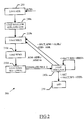
- the command interface reaches a starting state 205 in response to a specific input command CMD (for example, 0075h).
- a specific input command CMD for example, 0075h.
- the interface switches to a first loading state 210a, in which the input word WD and the input address ADR are loaded into the respective buffers.
- the input word WD is then latched into the first portion of the page buffer; at the same time, the starting address ADRs and the internal address ADRi are both set to the input address ADR.
- the command interface switches in succession to a sequence of further loading states 210b, 210c and 210d.
- the input word WD is loaded into the I/O buffer and is latched into the corresponding portion of the page buffer.
- the flag SR.0 is asserted (for signaling to the programming device that the flash memory cannot accept further input words WD); at the same time, the execution of a programming operation on the matrix is started.
- the programming operation involves a writing phase, wherein all the words of the page PG are written simultaneously into the set of locations selected by the internal address ADRi.
- the writing phase is immediately followed by a verification phase.
- the written page PGw (read with a safety margin from the matrix) is compared with the desired page PG. If the result of the verification is negative, the controller attempts to re-write the relevant memory cells until the page PG is written correctly (with the programming operation that fails after a predetermined number of attempts).
- the command interface switches to a further first loading state 215a, and simultaneously de-asserts the flag SR.0 (for allowing the programming device to provide further input words WD).
- this state 215a the input word WD and the input address ADR are loaded into the respective buffers.
- the command interface switches to a final state 220 (irrespective of the input information). Instead, when the end of the sector has not been reached yet, the command interface verifies whether the new input address ADR identifies the current sector (by means of a comparison with the internal address ADRi or the starting address ADRs). If the result of the verification is positive, the command interface returns to the state 210b and simultaneously drives the latching of the input word WD into the first portion of the page buffer.
- the internal address ADRi is automatically incremented so as to address the immediately following set of locations (ADRi+4); instead, if a new input address ADR has been provided (different from the starting address ADRs but always in the same sector), the internal address ADRi is set to the new input address ADR (skipping one or more sets of locations in the sector).
- the command interface verifies whether an input command CMD, specific for ending the programming procedure, has been provided (for example, FFFFh). If the result of the verification is positive, the command interface switches to the final state 220. On the contrary, the command interface remains in the state 215a (so that the unintentional writing of another sector is prevented).
- the concepts of the present invention are also applicable when the command interface implements a different state diagram, when the verification of the written page is executed in another way, when some actions are driven at different times (for example, providing additional dedicated states), and the like.
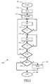
- the programming procedure of the flash memory is implemented by the execution of a method 300 under the control of the programming device.
- the method starts at block 305, and then passes to block 310 in which the programming device provides the command 0075h to the flash memory.
- the programming device transmits the first word to be written and the starting address for the programming procedure to the flash memory.
- the method then performs a loop, which involves the operation at block 315 of providing a further word to be written to the flash memory.
- a loop which involves the operation at block 315 of providing a further word to be written to the flash memory.
- the output condition of the cycle is satisfied at control block 320. Consequently, the method proceeds to block 325, in which the programming device polls the flag SR.0.
- a test is executed at decision block 330 to determine whether the programming operation has been completed (flag SR.0 de-asserted). If not, the method returns to block 325 in a waiting loop.
- the programming device at block 335 verifies whether the last desired page has been provided to the flash memory. If not, the method returns to block 315 for executing the same operations on a next page.
- the method enters decision block 340. If the end of the current sector has not been reached, the programming device at block 345 provides the command FFFFh to the flash memory; the method then ends at the final block 350; otherwise, the method descends into the final block 350 directly.
- the concepts of the present invention are also applicable when the programming procedure implements another equivalent method, when additional steps are provided (for example, with the programming device that verifies, by reading the state register, a total result of the programming procedure at the end thereof), and the like.
- the present invention proposes a non-volatile memory device suitable to be programmed in a sequential mode.
- the device includes a plurality of blocks of memory cells each one for storing a word; each block is identified by an address.
- Means is provided for loading an input address at the beginning of a programming procedure. Other means is used for setting an internal address to the input address.
- the device of the invention further includes means for loading a predetermined number of input words in succession.
- Means is provided for latching a page consisting of the predetermined number of input words.
- Other means is used for executing a programming operation; this operation includes writing the page in the blocks identified by consecutive addresses starting from the internal address. At the end, means is included for incrementing the internal address of the predetermined number in response to the completion of the programming operation.
- the memory device according to the present invention offers an improved sequential programming speed; without detracting from the general applicability of the invention, this advantage is particularly evident when the memory device has a high capacity.
- the memory device combines the advantages of a parallel multi-programming and of an internal management of the address; particularly, the programming device can supply the starting address of the programming procedure only once to the memory device.
- the proposed memory device supports a programming procedure that is specifically optimized for a production environment (even if other applications are not excluded). Particularly, this involves a high speed of a production line of the apparatuses that embody the memory devices; consequently, the yield of the production line is increased, with a corresponding reduction of the cost of those apparatuses.
- each page is verified (and re-written, if it is necessary) immediately after it has been written.
- a new input address is loaded at the completion of each programming operation.
- This feature is used to implement different modes of controlling the programming procedure.
- the programming procedure is terminated when the end of the current sector has been reached.
- the internal address is set to the new input address if this new input address identifies the current sector but is different from the starting address.
- the input word is discarded if the new input address does not identify the current sector.
- a flag for a busy state is asserted when all the words of a page have been loaded and is de-asserted when the programming operation has been completed.
- This flag is used to synchronize the operation of the programming device.
- the verification of the written words is executed in another way, the matrix of memory cells consists of a single sector, or the input address is loaded at the beginning of the programming procedure only. Furthermore, the programming procedure can continue on more sectors automatically or can be terminated in another way (for example, using a dedicated pin).
- the memory device of the present invention is also suitable to be implemented without supporting the possibility of skipping intermediate sets of locations, or without a mechanism for preventing the unintentional writing of other sectors; furthermore, it can be allowed jumping to a different sector, or a different mode of synchronization can be implemented (for example, exploiting a dedicated pin).
- the programming device that can be used to control the sequential programming of the above-described flash memory leads itself to be implemented even as a stand-alone product.
Landscapes
- Read Only Memory (AREA)
Abstract
Description
Claims (11)
- A non-volatile memory device (103) suitable to be programmed in a sequential mode including a plurality of blocks of memory cells (121) each one for storing a word, each block being identified by an address, means (124) for loading an input address at the beginning of a programming procedure and means (136,142) for setting an internal address to the input address,
characterized in that
the device further includes means (127) for loading a predetermined number of input words in succession, means (130-133) for latching a page consisting of the predetermined number of input words, means (145-157) for executing a programming operation including writing the page in the blocks identified by consecutive addresses starting from the internal address, and means (139,142) for incrementing the internal address of the predetermined number in response to the completion of the programming operation. - The device (103) according to claim 1, wherein the programming operation further includes verifying the written page and at least partially re-writing the page in response to a negative result of the verification.
- The device (103) according to claim 1 or 2, wherein the memory cells (121) are partitioned into a plurality of sectors, the writing operation being executed on a current sector, and wherein the device further includes means (124) for loading a new input address in response to the completion of the writing operation.
- The device (103) according to claim 3, further including means (154) for terminating the programming procedure when the internal address reaches an end of the current sector.
- The device (103) according to claim 3 or 4, further including means (154) for terminating the programming procedure if the new input address does not identify the current sector and the input word is equal to a predetermined value.
- The device (103) according to any claim from 3 to 5, further including means (135) for storing a starting address equal to the input address and means (142) for setting the internal address to the new input address if the new input address identifies the current sector and is different from the starting address.
- The device (103) according to any claim from 3 to 6, further including means (154) for discarding the input word if the new input address does not identify the current sector.
- The device (103) according to any claim from 3 to 7, further including means (154,160) for asserting a flag for a busy state of the device in response to the loading of the predetermined number of words and for de-asserting the flag in response to the completion of the programming operation.
- A method (200) of programming a non-volatile memory device in a sequential mode including a plurality of blocks of memory cells each one for storing a word, each block being identified by an address, the method including the steps of:characterized byloading (205) an input address at the beginning of a programming procedure, andsetting (205) an internal address to the input address,
repeating a plurality of times the steps of:loading (210a-210d) a predetermined number of input words in succession,latching (210a-210d) a page consisting of the predetermined number of input words,executing (210d) a programming operation including writing the page in the blocks identified by consecutive addresses starting from the internal address, andincrementing (215a) the internal address of the predetermined number in response to the completion of the programming operation. - A programming device (106) for controlling the programming in a sequential mode of a non-volatile memory device (103) including means (109,118) for providing an input address at the beginning of a programming procedure, means (115,118) for providing a predetermined number of input words in succession without increasing the input address, and means (109) for waiting for the completion of a programming operation of a page consisting of the predetermined number of input words.
- A method (300) of controlling the programming in a sequential mode of a non-volatile memory device including the steps of:and repeating a plurality of times the steps of:providing (312) an input address at the beginning of a programming procedure,providing (312-320;315-320) a predetermined number of input words in succession without increasing the input address, andwaiting (325-330) for the completion of a programming operation of a page consisting of the predetermined number of input words.
Applications Claiming Priority (2)
| Application Number | Priority Date | Filing Date | Title |
|---|---|---|---|
| ITMI20022668 | 2002-12-18 | ||
| IT002668A ITMI20022668A1 (en) | 2002-12-18 | 2002-12-18 | NON-VOLATILE MEMORY DEVICE WITH IMPROVED SPEED |
Publications (3)
| Publication Number | Publication Date |
|---|---|
| EP1434234A2 true EP1434234A2 (en) | 2004-06-30 |
| EP1434234A3 EP1434234A3 (en) | 2009-03-25 |
| EP1434234B1 EP1434234B1 (en) | 2016-03-09 |
Family
ID=32448924
Family Applications (1)
| Application Number | Title | Priority Date | Filing Date |
|---|---|---|---|
| EP03104713.7A Expired - Lifetime EP1434234B1 (en) | 2002-12-18 | 2003-12-16 | A non-volatile memory device with improved sequential programming speed |
Country Status (3)
| Country | Link |
|---|---|
| US (1) | US6940756B2 (en) |
| EP (1) | EP1434234B1 (en) |
| IT (1) | ITMI20022668A1 (en) |
Families Citing this family (2)
| Publication number | Priority date | Publication date | Assignee | Title |
|---|---|---|---|---|
| KR100891405B1 (en) * | 2007-09-27 | 2009-04-02 | 주식회사 하이닉스반도체 | Nonvolatile Memory Device and Its Operation Method |
| CN113886897B (en) * | 2020-07-03 | 2025-01-21 | 华邦电子股份有限公司 | Memory device and operation method for controlling non-volatile memory |
Family Cites Families (4)
| Publication number | Priority date | Publication date | Assignee | Title |
|---|---|---|---|---|
| TW231343B (en) * | 1992-03-17 | 1994-10-01 | Hitachi Seisakusyo Kk | |
| JP3310011B2 (en) * | 1992-03-30 | 2002-07-29 | 株式会社東芝 | Semiconductor memory and semiconductor memory board using the same |
| FR2803080A1 (en) * | 1999-12-22 | 2001-06-29 | St Microelectronics Sa | PAGE-BY-PAGE PROGRAMMABLE FLASH MEMORY |
| EP1308964B1 (en) * | 2001-10-25 | 2007-10-03 | STMicroelectronics S.r.l. | Fast programming method for nonvolatile memories, in particular flash memories, and related memory architecture |
-
2002
- 2002-12-18 IT IT002668A patent/ITMI20022668A1/en unknown
-
2003
- 2003-12-16 EP EP03104713.7A patent/EP1434234B1/en not_active Expired - Lifetime
- 2003-12-18 US US10/739,928 patent/US6940756B2/en not_active Expired - Lifetime
Also Published As
| Publication number | Publication date |
|---|---|
| EP1434234A3 (en) | 2009-03-25 |
| ITMI20022668A1 (en) | 2004-06-19 |
| EP1434234B1 (en) | 2016-03-09 |
| US6940756B2 (en) | 2005-09-06 |
| US20040165434A1 (en) | 2004-08-26 |
Similar Documents
| Publication | Publication Date | Title |
|---|---|---|
| US6542956B1 (en) | Latched address multi-chunk write to EEPROM | |
| US6016270A (en) | Flash memory architecture that utilizes a time-shared address bus scheme and separate memory cell access paths for simultaneous read/write operations | |
| US5822244A (en) | Method and apparatus for suspending a program/erase operation in a flash memory | |
| US6556504B2 (en) | Nonvolatile semiconductor memory device and data input/output control method thereof | |
| US6147905A (en) | Non-volatile semiconductor memory device | |
| US7808825B2 (en) | Non-volatile memory device and method of programming the same | |
| US7800971B2 (en) | Flash memory devices and methods of programming the same by overlapping programming operations for multiple mats | |
| US6552936B2 (en) | Semiconductor storage apparatus | |
| US7660177B2 (en) | Non-volatile memory device having high speed serial interface | |
| JP5101123B2 (en) | Burst read circuit and burst data output method for semiconductor memory device | |
| US8195993B2 (en) | Semiconductor integrated circuit device | |
| US20210193240A1 (en) | Semiconductor memory device | |
| US7689741B2 (en) | Dual buffer memory system for reducing data transmission time and control method thereof | |
| KR20150116174A (en) | Non-volatile memory device and method of operating the same | |
| US8086786B2 (en) | Non-volatile memory device and associated programming method | |
| US20060146612A1 (en) | Flash memory devices configured to output data without waiting for bitline and wordline recovery and methods of operating same | |
| US8045393B2 (en) | Program method of nonvolatile memory device | |
| US6940756B2 (en) | Non-volatile memory device with improved sequential programming speed | |
| KR100898653B1 (en) | Flash memory device and program method | |
| JP4652409B2 (en) | Storage device and storage device control method | |
| US7184310B2 (en) | Sequential program-verify method with result buffering | |
| JP2002133899A (en) | Non-volatile semiconductor memory and execution method for its auto-program | |
| US6029235A (en) | Automatic reloading of serial read pipeline on last bit transfers to serial access memory | |
| US7991945B2 (en) | Semiconductor memory device and semiconductor device | |
| JPWO2007023544A1 (en) | Storage device, storage device control method, and storage control device control method |
Legal Events
| Date | Code | Title | Description |
|---|---|---|---|
| PUAI | Public reference made under article 153(3) epc to a published international application that has entered the european phase |
Free format text: ORIGINAL CODE: 0009012 |
|
| AK | Designated contracting states |
Kind code of ref document: A2 Designated state(s): AT BE BG CH CY CZ DE DK EE ES FI FR GB GR HU IE IT LI LU MC NL PT RO SE SI SK TR |
|
| AX | Request for extension of the european patent |
Extension state: AL LT LV MK |
|
| PUAL | Search report despatched |
Free format text: ORIGINAL CODE: 0009013 |
|
| AK | Designated contracting states |
Kind code of ref document: A3 Designated state(s): AT BE BG CH CY CZ DE DK EE ES FI FR GB GR HU IE IT LI LU MC NL PT RO SE SI SK TR |
|
| AX | Request for extension of the european patent |
Extension state: AL LT LV MK |
|
| 17P | Request for examination filed |
Effective date: 20090624 |
|
| 17Q | First examination report despatched |
Effective date: 20090729 |
|
| AKX | Designation fees paid |
Designated state(s): DE |
|
| RAP1 | Party data changed (applicant data changed or rights of an application transferred) |
Owner name: STMICROELECTRONICS SRL |
|
| RAP1 | Party data changed (applicant data changed or rights of an application transferred) |
Owner name: STMICROELECTRONICS SRL |
|
| GRAP | Despatch of communication of intention to grant a patent |
Free format text: ORIGINAL CODE: EPIDOSNIGR1 |
|
| INTG | Intention to grant announced |
Effective date: 20150909 |
|
| GRAS | Grant fee paid |
Free format text: ORIGINAL CODE: EPIDOSNIGR3 |
|
| GRAA | (expected) grant |
Free format text: ORIGINAL CODE: 0009210 |
|
| AK | Designated contracting states |
Kind code of ref document: B1 Designated state(s): DE |
|
| REG | Reference to a national code |
Ref country code: DE Ref legal event code: R081 Ref document number: 60348619 Country of ref document: DE Owner name: MICRON TECHNOLOGY, INC., BOISE, US Free format text: FORMER OWNER: STMICROELECTRONICS S.R.L., AGRATE BRIANZA, IT |
|
| RAP2 | Party data changed (patent owner data changed or rights of a patent transferred) |
Owner name: STMICROELECTRONICS NV |
|
| REG | Reference to a national code |
Ref country code: DE Ref legal event code: R096 Ref document number: 60348619 Country of ref document: DE |
|
| RAP2 | Party data changed (patent owner data changed or rights of a patent transferred) |
Owner name: NUMONYX BV |
|
| RAP2 | Party data changed (patent owner data changed or rights of a patent transferred) |
Owner name: MICRON TECHNOLOGY, INC. |
|
| REG | Reference to a national code |
Ref country code: DE Ref legal event code: R081 Ref document number: 60348619 Country of ref document: DE Owner name: MICRON TECHNOLOGY, INC., BOISE, US Free format text: FORMER OWNER: STMICROELECTRONICS SRL, AGRATE BRIANZA, IT |
|
| REG | Reference to a national code |
Ref country code: DE Ref legal event code: R097 Ref document number: 60348619 Country of ref document: DE |
|
| PLBE | No opposition filed within time limit |
Free format text: ORIGINAL CODE: 0009261 |
|
| STAA | Information on the status of an ep patent application or granted ep patent |
Free format text: STATUS: NO OPPOSITION FILED WITHIN TIME LIMIT |
|
| 26N | No opposition filed |
Effective date: 20161212 |
|
| REG | Reference to a national code |
Ref country code: DE Ref legal event code: R082 Ref document number: 60348619 Country of ref document: DE Representative=s name: HOEGER, STELLRECHT & PARTNER PATENTANWAELTE MB, DE |
|
| PGFP | Annual fee paid to national office [announced via postgrant information from national office to epo] |
Ref country code: DE Payment date: 20220527 Year of fee payment: 20 |
|
| REG | Reference to a national code |
Ref country code: DE Ref legal event code: R071 Ref document number: 60348619 Country of ref document: DE |