EP1433872A1 - Method for forming resin film and method for manufacturing electronic parts - Google Patents
Method for forming resin film and method for manufacturing electronic parts Download PDFInfo
- Publication number
- EP1433872A1 EP1433872A1 EP02768070A EP02768070A EP1433872A1 EP 1433872 A1 EP1433872 A1 EP 1433872A1 EP 02768070 A EP02768070 A EP 02768070A EP 02768070 A EP02768070 A EP 02768070A EP 1433872 A1 EP1433872 A1 EP 1433872A1
- Authority
- EP
- European Patent Office
- Prior art keywords
- resin material
- polyethylene
- manufacturing
- resin film
- resin
- Prior art date
- Legal status (The legal status is an assumption and is not a legal conclusion. Google has not performed a legal analysis and makes no representation as to the accuracy of the status listed.)
- Withdrawn
Links
Images


Classifications
-
- B—PERFORMING OPERATIONS; TRANSPORTING
- B05—SPRAYING OR ATOMISING IN GENERAL; APPLYING FLUENT MATERIALS TO SURFACES, IN GENERAL
- B05D—PROCESSES FOR APPLYING FLUENT MATERIALS TO SURFACES, IN GENERAL
- B05D1/00—Processes for applying liquids or other fluent materials
- B05D1/60—Deposition of organic layers from vapour phase
-
- C—CHEMISTRY; METALLURGY
- C23—COATING METALLIC MATERIAL; COATING MATERIAL WITH METALLIC MATERIAL; CHEMICAL SURFACE TREATMENT; DIFFUSION TREATMENT OF METALLIC MATERIAL; COATING BY VACUUM EVAPORATION, BY SPUTTERING, BY ION IMPLANTATION OR BY CHEMICAL VAPOUR DEPOSITION, IN GENERAL; INHIBITING CORROSION OF METALLIC MATERIAL OR INCRUSTATION IN GENERAL
- C23C—COATING METALLIC MATERIAL; COATING MATERIAL WITH METALLIC MATERIAL; SURFACE TREATMENT OF METALLIC MATERIAL BY DIFFUSION INTO THE SURFACE, BY CHEMICAL CONVERSION OR SUBSTITUTION; COATING BY VACUUM EVAPORATION, BY SPUTTERING, BY ION IMPLANTATION OR BY CHEMICAL VAPOUR DEPOSITION, IN GENERAL
- C23C14/00—Coating by vacuum evaporation, by sputtering or by ion implantation of the coating forming material
- C23C14/06—Coating by vacuum evaporation, by sputtering or by ion implantation of the coating forming material characterised by the coating material
- C23C14/12—Organic material
-
- H—ELECTRICITY
- H01—ELECTRIC ELEMENTS
- H01B—CABLES; CONDUCTORS; INSULATORS; SELECTION OF MATERIALS FOR THEIR CONDUCTIVE, INSULATING OR DIELECTRIC PROPERTIES
- H01B1/00—Conductors or conductive bodies characterised by the conductive materials; Selection of materials as conductors
- H01B1/20—Conductive material dispersed in non-conductive organic material
- H01B1/24—Conductive material dispersed in non-conductive organic material the conductive material comprising carbon-silicon compounds, carbon or silicon
-
- H—ELECTRICITY
- H01—ELECTRIC ELEMENTS
- H01C—RESISTORS
- H01C17/00—Apparatus or processes specially adapted for manufacturing resistors
- H01C17/06—Apparatus or processes specially adapted for manufacturing resistors adapted for coating resistive material on a base
- H01C17/065—Apparatus or processes specially adapted for manufacturing resistors adapted for coating resistive material on a base by thick film techniques, e.g. serigraphy
- H01C17/06506—Precursor compositions therefor, e.g. pastes, inks, glass frits or green body
- H01C17/06573—Precursor compositions therefor, e.g. pastes, inks, glass frits or green body characterised by the permanent binder
- H01C17/06586—Precursor compositions therefor, e.g. pastes, inks, glass frits or green body characterised by the permanent binder composed of organic material
-
- H—ELECTRICITY
- H01—ELECTRIC ELEMENTS
- H01C—RESISTORS
- H01C7/00—Non-adjustable resistors formed as one or more layers or coatings; Non-adjustable resistors made from powdered conducting material or powdered semi-conducting material with or without insulating material
- H01C7/02—Non-adjustable resistors formed as one or more layers or coatings; Non-adjustable resistors made from powdered conducting material or powdered semi-conducting material with or without insulating material having positive temperature coefficient
- H01C7/027—Non-adjustable resistors formed as one or more layers or coatings; Non-adjustable resistors made from powdered conducting material or powdered semi-conducting material with or without insulating material having positive temperature coefficient consisting of conducting or semi-conducting material dispersed in a non-conductive organic material
-
- H—ELECTRICITY
- H05—ELECTRIC TECHNIQUES NOT OTHERWISE PROVIDED FOR
- H05K—PRINTED CIRCUITS; CASINGS OR CONSTRUCTIONAL DETAILS OF ELECTRIC APPARATUS; MANUFACTURE OF ASSEMBLAGES OF ELECTRICAL COMPONENTS
- H05K1/00—Printed circuits
- H05K1/16—Printed circuits incorporating printed electric components, e.g. printed resistors, capacitors or inductors
- H05K1/162—Printed circuits incorporating printed electric components, e.g. printed resistors, capacitors or inductors incorporating printed capacitors
Definitions
- the present invention relates to a method for manufacturing a resin film and a method for manufacturing an electronic component.
- Resin films are used in various fields. For example, they are used as a constituent member of an electronic component such as a capacitor or a PTC thermistor. In general, such resin films have been formed by the application of a resin dissolved in a solvent. In recent years, as electronic components have become smaller and achieved a higher performance than ever, there has been an increasing demand for the formation of a thin resin film in a highly controllable manner.
- a thin film has been difficult to form with excellent controllability by the forming method with the solvent application.
- a conventional method for forming a resin film by vapor deposition has only allowed the deposition of resins with a number-average molecular weight of about 300. If resins with a higher molecular weight are to be deposited, heating at a high temperature is necessary, which modifies the resin property. Consequently, there has been a problem that the resin serving as a deposition source and a resin that has been deposited have different properties.
- a method for manufacturing a resin film of the present invention is a method for manufacturing a resin film by a vapor deposition of a resin material.
- the method includes depositing the resin material by heating the resin material at a heating temperature higher than a melting point of the resin material in a reduced pressure atmosphere.
- the resin material may has a viscosity-average molecular weight ranging from 500 to 1000000, for example.
- a resin material undergoes oxidation, which causes a deterioration of the resin property.
- the heating temperature is higher than a decomposition temperature of the resin material in an ambient atmosphere (atmospheric air) and lower than a decomposition temperature of the resin material in the reduced pressure atmosphere.
- the "decomposition temperature” in the present specification refers to a temperature at which the property of the resin material deteriorates owing to oxidation or the like.
- the resin material may be a polyethylene whose viscosity-average molecular weight ranges from 500 to 10000.
- the heating temperature (°C) is 2.8 to 3.8 times as high as a melting point (°C) of the polyethylene.
- an electronic component of the present invention is an electronic component including a resin film.
- the resin film is formed of a resin material whose viscosity-average molecular weight ranges from 500 to 1000000, and the resin film has a thickness ranging from 0.01 to 1 ⁇ m.
- the manufacture of this electronic component is first made possible by the manufacturing method of the present invention. Further, electrically conductive particles or the like may be contained in the resin film.
- the above-described electronic component may further include a first electrode and a second electrode that are arranged so as to sandwich the resin film, and electrically conductive particles arranged inside the resin film.
- the resin material may be a polyethylene whose viscosity-average molecular weight ranges from 500 to 10000. With this structure, it is possible to obtain a PTC thermistor including a thin polyethylene film.
- a method for manufacturing an electronic component according to the present invention is a method for manufacturing an electronic component including a resin film formed of a resin material.
- the method includes forming the resin film by a deposition of the resin material by heating the resin material at a heating temperature higher than a melting point of the resin material in a reduced pressure atmosphere.
- the resin material has a viscosity-average molecular weight ranging from 500 to 1000000, for example.
- This manufacturing method uses the above-described method for manufacturing a resin film. With this manufacturing method, a thin resin film can be formed with excellent controllability, so that a thin electronic component can be manufactured reliably. Furthermore, since the resin film has substantially the same property as the resin material serving as a material for the resin film, it is possible to manufacture an electronic component with an excellent property.
- the heating temperature is lower than a decomposition temperature of the resin material in the reduced pressure atmosphere.
- the resin material may be a polyethylene whose viscosity-average molecular weight ranges from 500 to 10000.
- the heating temperature (°C) is 2.8 to 3.8 times as high as a melting point (°C) of the polyethylene.
- the first embodiment is directed to a method for manufacturing a resin film according to the present invention.
- a resin material in the following, sometimes referred to as a resin material A
- the resin material A is placed in a reduced pressure chamber, or a chamber in which the resin material A is previously provided is decompressed.
- the method of the present invention deposits the resin material A in the reduced pressure atmosphere.
- the resin film may be cross-linked by an electron beam irradiation or the like.
- the viscosity-average molecular weight of the resin material A ranges, for example, from 100 to 1000000 (for example 500 to 1000000) and, preferably, from 500 to 5000.
- the resin material A can be polyethylene (PE), polypropylene (PP), polystyrene (PS), polymethyl methacrylate (PMMA), polyvinyl alcohol (PVA) or polyvinyl butyral (PVB), for example.
- the resin material A can be deposited by (i) arranging the resin material A in a container that can be decompressed, (ii) decompressing the container and (iii) heating the resin material A up to a temperature higher than its melting point. At this time, substances that evaporate at a temperature lower than the melting point are considered as impurities in the resin material A. When such substances are mixed in a resin film, desired characteristics cannot be obtained in some cases.
- the pressure in the container at the time of deposition varies depending on a measuring position, it is not greater than 1.0 ⁇ 10 -1 Pa, for example, and ranges from 1.0 ⁇ 10 -3 Pa to 1.0 ⁇ 10 -1 Pa, more specifically.
- the pressure near an evaporation location for the resin material A is about 1 to 10 Pa, for example.
- the heating temperature of the resin material A is higher than a decomposition temperature of the resin material A in an ambient atmosphere (atmospheric air) and lower than a decomposition temperature thereof in the reduced pressure atmosphere (at a pressure inside the container).
- the ambient atmosphere atmospheric air refers to air at 1 atmospheric pressure (1.01 ⁇ 10 5 Pa).
- the resin material A since the resin material A is heated in the reduced pressure atmosphere, it can be heated at a temperature higher than the decomposition temperature thereof in an ambient atmospheric.
- the heating temperature is 2.8 to 3.8 times (more preferably, 2.8 to 3.4 times) as high as the melting point of the polyethylene or ranges from 350°C to 480°C (more preferably, 350°C to 425°C).
- the heating temperature may be 2 to 4.5 times as high as the melting point of the polyethylene depending on the pressure in the chamber.
- the heating temperature may be 2 to 4.5 times (preferably, 2.8 to 3.8 times) as high as the melting point of the resin material.
- a resin film as thin as, for example, 0.01 to 1.0 ⁇ m (generally, 0.05 to 0.5 ⁇ m) can be formed with excellent controllability.
- the second embodiment is directed to an example of an electronic component of the present invention and a method for manufacturing the same.
- the electronic component of the present invention includes a resin film, which is manufactured by the manufacturing method of the first embodiment.
- the method of the present invention for manufacturing an electronic component includes a process of manufacturing a resin film by the manufacturing method described in the first embodiment.
- a PTC thermistor and a method for manufacturing the same will be described as an example of the electronic component of the present invention and the method for manufacturing the same.
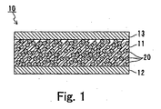
- Fig. 1 shows a cross-section of a PTC thermistor 10 of the second embodiment.
- the PTC thermistor 10 includes a polyethylene film 11 containing electrically conductive particles 20, and a first electrode 12 and a second electrode 13 that are arranged so as to sandwich the polyethylene film 11.
- the polyethylene film 11 is made of polyethylene whose viscosity-average molecular weight ranges from 100 to 10000 (preferably 500 to 10000), and has a thickness ranging from 0.01 to 1 ⁇ m.
- the electrically conductive particles 20 contained in the polyethylene film 11 can be, for example, carbon particles having a particle diameter of about 0.01 to 0.05 ⁇ m.
- the electrically conductive particles distributed in the polyethylene film 11 control an electrical conductivity between the first electrode 12 and the second electrode 13. Therefore, an increase in the temperature causes the polyethylene film 11 to expand so as to increase an average distance between the electrically conductive particles, thus increasing the resistance between the first electrode 12 and the second electrode 13. Accordingly, the PTC thermistor 10 has a positive temperature coefficient (PTC).
- the first electrode 12 and the second electrode 13 can be formed of an electrically conductive material, for example, a metal foil or a metal film. More specifically, a metal foil made of Al, Ni, Cu, Ag, Au or an alloy thereof can be used, for example.
- the polyethylene film 11 containing the electrically conductive particles 20 first is formed on the first electrode 12.
- the polyethylene film 11 is made of polyethylene (in the following, sometimes referred to as a polyethylene A) whose viscosity-average molecular weight ranges from 100 to 10000 (preferably 500 to 10000).
- the polyethylene film 11 is formed by heating the polyethylene A at the heating temperature higher than the melting point thereof and depositing the polyethylene A on the first electrode 12, in the reduced pressure atmosphere.
- the electrically conductive particles also are evaporated at the same time as the polyethylene A, thereby forming the polyethylene film 11 containing the electrically conductive particles.
- the vapor deposition can be carried out by a manufacturing apparatus 30, which will be described later in the example.
- the heating temperature of the polyethylene A at the time of deposition is higher than a decomposition temperature of the polyethylene A in an ambient atmosphere and lower than a decomposition temperature thereof in the reduced pressure atmosphere. More specifically, it is preferable that the heating temperature of the polyethylene A at the time of deposition is 2.8 to 3.8 times (more preferably, 2.8 to 3.4 times) as high as the melting point of the polyethylene A or ranges from 350°C to 480°C (more preferably, 350°C to 425°C).
- the pressure at the time of deposition varies depending on a measuring position, it is not greater than 1.0 ⁇ 10 -1 Pa, for example, and ranges from 1.0 ⁇ 10 -3 Pa to 1.0 ⁇ 10 -1 Pa, more specifically.
- the pressure near an evaporation location of the polyethylene A is about 1 to 10 Pa, for example.
- the second electrode 13 is formed on the polyethylene film 11.
- the second electrode 13 can be formed by vapor deposition, for example. In this manner, the PTC thermistor 10 can be manufactured.
- the present invention also can be applied to an electronic component including a resin film formed of a resin material whose viscosity-average molecular weight ranges from 100 to 1000000 (for example 500 to 1000000, preferably 500 to 5000). More specifically, it can be applied to a resistor, a sensor or a battery, for example.
- the second embodiment has been directed to the case where the resin material is polyethylene, the resin material also can be any resin material described in the first embodiment.
- FIG. 3 schematically shows a manufacturing apparatus used in the present example, with the hatching being partially omitted.
- a manufacturing apparatus 30 shown in Fig. 3 includes a container 50 that can be decompressed, a cooling roller 31 arranged inside the container 50 , crucibles 32 to 34, shutters 35 to 37 and a device 38 for cross-linking a resin material.
- the device 38 can be, for example, an electron gun emitting an electron beam.
- the cooling roller 31 rotates in a direction indicated by an arrow B.
- An electrode material 39, electrically conductive particles 40 and a resin material 41 respectively are provided in the crucibles 32, 33 and 34, which can be heated independently.
- the shutters 35 to 37 prevent substances that have been evaporated from the crucibles 32 to 34, from reaching the cooling roller 31 as necessary. In this case, the vapor deposition is performed such that the shutter of the crucible 34 containing the resin material is opened after the crucible is heated up to a desired temperature. This makes it possible to evaporate only a desired component out of the resin material having a broad molecular distribution.
- the substances that have been evaporated from the crucibles 32 to 34 are deposited on the cooling roller 31.
- the electrode material 39 is evaporated from the crucible 32, thus depositing the first electrode on the cooling roller 31. Then, the electrically conductive particles 40 and the resin material 41 are evaporated respectively from the crucibles 33 and 34, thus depositing the resin film containing the electrically conductive particles on the first electrode. Simultaneously, the formed resin film is cross-linked by an irradiation with an electron beam emitted from the device 38. Finally, the electrode material 39 is evaporated from the crucible 32, thus forming the second electrode on the resin film. In this manner, the PTC thermistor 10 is manufactured.
- a resin film made solely of polyethylene whose viscosity-average molecular weight was 2000 (melting point: 125°C) was formed by vapor deposition using the manufacturing apparatus 30.
- the decomposition temperature of this polyethylene in the ambient atmosphere (atmospheric air) was about 300°C.
- the pressure at the evaporation location inside the container was set to be 1 to 10 Pa, and the heating temperature of the crucible 34 containing the polyethylene as a material was changed between 150°C and 500°C. Then, the melting points of the formed polyethylene film and the polyethylene remaining in the crucible 34 were measured.
- FIG. 4 shows the relationship between the heating temperature of the crucible 34 and the melting points of the formed polyethylene film and the polyethylene remaining in the crucible 34.
- the heating temperature within the range of 350°C to 480°C (the range of 2.8 to 3.8 times as high as the melting point of the polyethylene serving as the material), it was possible to form a polyethylene film whose melting point is substantially equal to that of the polyethylene before the deposition.
- the method of the present invention makes it possible to form a polyethylene film maintaining the property of the polyethylene serving as the material.
- the method according to the present invention forms a film by vapor deposition, a thin polyethylene film can be formed with excellent controllability.
- a thin resin film can be formed with excellent controllability. Also, according to the method of the present invention for manufacturing an electronic component, an electronic component including a thin resin film can be manufactured with excellent controllability.
Landscapes
- Engineering & Computer Science (AREA)
- Chemical & Material Sciences (AREA)
- Microelectronics & Electronic Packaging (AREA)
- Dispersion Chemistry (AREA)
- Physics & Mathematics (AREA)
- Metallurgy (AREA)
- Materials Engineering (AREA)
- Mechanical Engineering (AREA)
- Chemical Kinetics & Catalysis (AREA)
- Organic Chemistry (AREA)
- Ceramic Engineering (AREA)
- Spectroscopy & Molecular Physics (AREA)
- Manufacturing & Machinery (AREA)
- Electromagnetism (AREA)
- Physical Vapour Deposition (AREA)
- Thermistors And Varistors (AREA)
- Internal Circuitry In Semiconductor Integrated Circuit Devices (AREA)
- Fixed Capacitors And Capacitor Manufacturing Machines (AREA)
- Compositions Of Macromolecular Compounds (AREA)
Abstract
A method for manufacturing a resin film according to the present
invention includes depositing the resin material by heating a resin material
at a heating temperature higher than a melting point of the resin material
in a reduced pressure atmosphere. The resin material may have a
viscosity-average molecular weight ranging from 500 to 1000000.
Furthermore, a method for manufacturing an electronic component
according to the present invention uses this method for manufacturing the
resin film. In accordance with the present invention, a thin resin film can
be manufactured with excellent controllability, so that an electronic
component including such a resin film can be obtained.
Description
The present invention relates to a method for manufacturing a
resin film and a method for manufacturing an electronic component.
Resin films are used in various fields. For example, they are used
as a constituent member of an electronic component such as a capacitor or a
PTC thermistor. In general, such resin films have been formed by the
application of a resin dissolved in a solvent. In recent years, as electronic
components have become smaller and achieved a higher performance than
ever, there has been an increasing demand for the formation of a thin resin
film in a highly controllable manner.
However, a thin film has been difficult to form with excellent
controllability by the forming method with the solvent application. On the
other hand, a conventional method for forming a resin film by vapor
deposition has only allowed the deposition of resins with a number-average
molecular weight of about 300. If resins with a higher molecular weight
are to be deposited, heating at a high temperature is necessary, which
modifies the resin property. Consequently, there has been a problem that
the resin serving as a deposition source and a resin that has been deposited
have different properties.
With the foregoing in mind, it is an object of the present invention to
provide a new method for manufacturing a resin film, a method for
manufacturing an electronic component using the same, and a new
electronic component obtained by this method. In the following description,
heating temperatures and melting points are expressed in centigrade (°C).
In order to achieve the above-mentioned object, a method for
manufacturing a resin film of the present invention is a method for
manufacturing a resin film by a vapor deposition of a resin material. The
method includes depositing the resin material by heating the resin material
at a heating temperature higher than a melting point of the resin material
in a reduced pressure atmosphere. The resin material may has a
viscosity-average molecular weight ranging from 500 to 1000000, for
example. Conventionally, it has been known that, when heated at a
temperature higher than its melting point, a resin material undergoes
oxidation, which causes a deterioration of the resin property. Therefore, no
attempt has been made to form a resin film by depositing a resin material
with a viscosity-average molecular weight equal to or greater than 500.
Under such circumstances, the inventors of the present invention have
found that heating in the reduced pressure atmosphere enables the vapor
deposition without any deterioration of the resin material. The method
of the present invention for manufacturing a resin film is based on this
new finding and uses the vapor deposition, which had not been used
conventionally, as a method for manufacturing a resin film formed of an
organic molecules whose viscosity-average molecular weight is equal to or
greater than 500. This allows a thin resin film to be manufactured with
excellent controllability.
In the above-described method for manufacturing a resin film, it is
preferable that the heating temperature is higher than a decomposition
temperature of the resin material in an ambient atmosphere (atmospheric
air) and lower than a decomposition temperature of the resin material in the
reduced pressure atmosphere. The "decomposition temperature" in the
present specification refers to a temperature at which the property of the
resin material deteriorates owing to oxidation or the like.
In the above-described method for manufacturing a resin film, the
resin material may be a polyethylene whose viscosity-average molecular
weight ranges from 500 to 10000. In this case, it is preferable that the
heating temperature (°C) is 2.8 to 3.8 times as high as a melting point (°C)
of the polyethylene. With this structure, it is possible to form a
polyethylene film having substantially the same property as the
polyethylene before the deposition.
Furthermore, an electronic component of the present invention is an
electronic component including a resin film. The resin film is formed of a
resin material whose viscosity-average molecular weight ranges from 500
to 1000000, and the resin film has a thickness ranging from 0.01 to 1 µm.
The manufacture of this electronic component is first made possible by the
manufacturing method of the present invention. Further, electrically
conductive particles or the like may be contained in the resin film.
The above-described electronic component may further include a
first electrode and a second electrode that are arranged so as to sandwich
the resin film, and electrically conductive particles arranged inside the resin
film. The resin material may be a polyethylene whose viscosity-average
molecular weight ranges from 500 to 10000. With this structure, it is
possible to obtain a PTC thermistor including a thin polyethylene film.
Moreover, a method for manufacturing an electronic component
according to the present invention is a method for manufacturing an
electronic component including a resin film formed of a resin material.
The method includes forming the resin film by a deposition of the resin
material by heating the resin material at a heating temperature higher
than a melting point of the resin material in a reduced pressure atmosphere.
The resin material has a viscosity-average molecular weight ranging from
500 to 1000000, for example. This manufacturing method uses the
above-described method for manufacturing a resin film. With this
manufacturing method, a thin resin film can be formed with excellent
controllability, so that a thin electronic component can be manufactured
reliably. Furthermore, since the resin film has substantially the same
property as the resin material serving as a material for the resin film, it is
possible to manufacture an electronic component with an excellent property.
In the above-described method for manufacturing an electronic
component, it is preferable that the heating temperature is lower than a
decomposition temperature of the resin material in the reduced pressure
atmosphere.
In the above-described method for manufacturing an electronic
component, the resin material may be a polyethylene whose
viscosity-average molecular weight ranges from 500 to 10000. In this
case, it is preferable that the heating temperature (°C) is 2.8 to 3.8 times as
high as a melting point (°C) of the polyethylene.
The following is a description of preferred embodiments of the
present invention, with reference to the accompanying drawings.
The first embodiment is directed to a method for manufacturing a
resin film according to the present invention. In the manufacturing
method of the first embodiment, first, a resin material (in the following,
sometimes referred to as a resin material A) is provided in a reduced
pressure atmosphere. For example, the resin material A is placed in a
reduced pressure chamber, or a chamber in which the resin material A is
previously provided is decompressed.
Next, in this reduced pressure atmosphere, by heating the resin
material A at a heating temperature higher than a melting point of the resin
material A, the resin material A is evaporated and then deposited on a base
(a substrate, an electrode or the like), thus forming a resin film. In other
words, the method of the present invention deposits the resin material A in
the reduced pressure atmosphere. After the resin film is formed by
depositing the resin material, the resin film may be cross-linked by an
electron beam irradiation or the like.
The viscosity-average molecular weight of the resin material A
ranges, for example, from 100 to 1000000 (for example 500 to 1000000) and,
preferably, from 500 to 5000. The resin material A can be polyethylene
(PE), polypropylene (PP), polystyrene (PS), polymethyl methacrylate
(PMMA), polyvinyl alcohol (PVA) or polyvinyl butyral (PVB), for example.
The resin material A can be deposited by (i) arranging the resin
material A in a container that can be decompressed, (ii) decompressing the
container and (iii) heating the resin material A up to a temperature higher
than its melting point. At this time, substances that evaporate at a
temperature lower than the melting point are considered as impurities in
the resin material A. When such substances are mixed in a resin film,
desired characteristics cannot be obtained in some cases. Although the
pressure in the container at the time of deposition varies depending on a
measuring position, it is not greater than 1.0 × 10⁻¹ Pa, for example, and
ranges from 1.0 × 10⁻³ Pa to 1.0 × 10⁻¹ Pa, more specifically. The pressure
near an evaporation location for the resin material A is about 1 to 10 Pa, for
example.
It is preferable that the heating temperature of the resin material A
is higher than a decomposition temperature of the resin material A in an
ambient atmosphere (atmospheric air) and lower than a decomposition
temperature thereof in the reduced pressure atmosphere (at a pressure
inside the container). Herein, the ambient atmosphere (atmospheric air)
refers to air at 1 atmospheric pressure (1.01 × 10⁵ Pa). In the
manufacturing method of the present invention, since the resin material A is
heated in the reduced pressure atmosphere, it can be heated at a
temperature higher than the decomposition temperature thereof in an
ambient atmospheric. When the resin material A is polyethylene with a
viscosity-average molecular weight ranging from 100 to 10000 (for example,
500 to 10000, preferably 500 to 5000), it is preferable that the heating
temperature is 2.8 to 3.8 times (more preferably, 2.8 to 3.4 times) as high as
the melting point of the polyethylene or ranges from 350°C to 480°C (more
preferably, 350°C to 425°C). The heating temperature may be 2 to 4.5
times as high as the melting point of the polyethylene depending on the
pressure in the chamber. For other resin material, the heating
temperature may be 2 to 4.5 times (preferably, 2.8 to 3.8 times) as high as
the melting point of the resin material.
In accordance with this manufacturing method, a resin film as thin
as, for example, 0.01 to 1.0 µm (generally, 0.05 to 0.5 µm) can be formed with
excellent controllability.
The second embodiment is directed to an example of an electronic
component of the present invention and a method for manufacturing the
same. The electronic component of the present invention includes a resin
film, which is manufactured by the manufacturing method of the first
embodiment. The method of the present invention for manufacturing an
electronic component includes a process of manufacturing a resin film by the
manufacturing method described in the first embodiment.
In the following, a PTC thermistor and a method for manufacturing
the same will be described as an example of the electronic component of the
present invention and the method for manufacturing the same. Fig. 1
shows a cross-section of a PTC thermistor 10 of the second embodiment.
Referring to Fig. 1, the PTC thermistor 10 includes a polyethylene
film 11 containing electrically conductive particles 20, and a first electrode
12 and a second electrode 13 that are arranged so as to sandwich the
polyethylene film 11.
The polyethylene film 11 is made of polyethylene whose
viscosity-average molecular weight ranges from 100 to 10000 (preferably
500 to 10000), and has a thickness ranging from 0.01 to 1 µm. The
electrically conductive particles 20 contained in the polyethylene film 11 can
be, for example, carbon particles having a particle diameter of about 0.01 to
0.05 µm. In the PTC thermistor 10, the electrically conductive particles
distributed in the polyethylene film 11 control an electrical conductivity
between the first electrode 12 and the second electrode 13. Therefore, an
increase in the temperature causes the polyethylene film 11 to expand so as
to increase an average distance between the electrically conductive particles,
thus increasing the resistance between the first electrode 12 and the second
electrode 13. Accordingly, the PTC thermistor 10 has a positive
temperature coefficient (PTC).
The first electrode 12 and the second electrode 13 can be formed of
an electrically conductive material, for example, a metal foil or a metal film.
More specifically, a metal foil made of Al, Ni, Cu, Ag, Au or an alloy thereof
can be used, for example.
The following is a description of a method for manufacturing the
PTC thermistor 10, with reference to Fig. 2. In this manufacturing method,
as shown in Fig. 2A, the polyethylene film 11 containing the electrically
conductive particles 20 first is formed on the first electrode 12. The
polyethylene film 11 is made of polyethylene (in the following, sometimes
referred to as a polyethylene A) whose viscosity-average molecular weight
ranges from 100 to 10000 (preferably 500 to 10000). The polyethylene film
11 is formed by heating the polyethylene A at the heating temperature
higher than the melting point thereof and depositing the polyethylene A on
the first electrode 12, in the reduced pressure atmosphere. At this time,
the electrically conductive particles also are evaporated at the same time as
the polyethylene A, thereby forming the polyethylene film 11 containing the
electrically conductive particles. The vapor deposition can be carried out
by a manufacturing apparatus 30, which will be described later in the
example.
It is preferable that the heating temperature of the polyethylene A
at the time of deposition is higher than a decomposition temperature of the
polyethylene A in an ambient atmosphere and lower than a decomposition
temperature thereof in the reduced pressure atmosphere. More specifically,
it is preferable that the heating temperature of the polyethylene A at the
time of deposition is 2.8 to 3.8 times (more preferably, 2.8 to 3.4 times) as
high as the melting point of the polyethylene A or ranges from 350°C to
480°C (more preferably, 350°C to 425°C). Although the pressure at the
time of deposition varies depending on a measuring position, it is not
greater than 1.0 × 10⁻¹ Pa, for example, and ranges from 1.0 × 10⁻³ Pa to 1.0
× 10-1 Pa, more specifically. The pressure near an evaporation location of
the polyethylene A is about 1 to 10 Pa, for example.
Subsequently, as shown in Fig. 2B, the second electrode 13 is formed
on the polyethylene film 11. The second electrode 13 can be formed by
vapor deposition, for example. In this manner, the PTC thermistor 10 can
be manufactured.
Although the second embodiment has been directed to the PTC
thermistor, the present invention also can be applied to an electronic
component including a resin film formed of a resin material whose
viscosity-average molecular weight ranges from 100 to 1000000 (for
example 500 to 1000000, preferably 500 to 5000). More specifically, it can
be applied to a resistor, a sensor or a battery, for example. Furthermore,
although the second embodiment has been directed to the case where the
resin material is polyethylene, the resin material also can be any resin
material described in the first embodiment.
The following is a further specific description of the present
invention by way of an example. In this example, an exemplary case of
forming a resin film by the manufacturing method of the present invention
will be described.
Fig. 3 schematically shows a manufacturing apparatus used in the
present example, with the hatching being partially omitted. A
manufacturing apparatus 30 shown in Fig. 3 includes a container 50 that
can be decompressed, a cooling roller 31 arranged inside the container 50 ,
crucibles 32 to 34, shutters 35 to 37 and a device 38 for cross-linking a resin
material. The device 38 can be, for example, an electron gun emitting an
electron beam.
The cooling roller 31 rotates in a direction indicated by an arrow B.
An electrode material 39, electrically conductive particles 40 and a resin
material 41 respectively are provided in the crucibles 32, 33 and 34, which
can be heated independently. The shutters 35 to 37 prevent substances
that have been evaporated from the crucibles 32 to 34, from reaching the
cooling roller 31 as necessary. In this case, the vapor deposition is
performed such that the shutter of the crucible 34 containing the resin
material is opened after the crucible is heated up to a desired temperature.
This makes it possible to evaporate only a desired component out of the
resin material having a broad molecular distribution. The substances that
have been evaporated from the crucibles 32 to 34 are deposited on the
cooling roller 31. When manufacturing the PTC thermistor 10, first, the
electrode material 39 is evaporated from the crucible 32, thus depositing the
first electrode on the cooling roller 31. Then, the electrically conductive
particles 40 and the resin material 41 are evaporated respectively from the
crucibles 33 and 34, thus depositing the resin film containing the electrically
conductive particles on the first electrode. Simultaneously, the formed
resin film is cross-linked by an irradiation with an electron beam emitted
from the device 38. Finally, the electrode material 39 is evaporated from
the crucible 32, thus forming the second electrode on the resin film. In this
manner, the PTC thermistor 10 is manufactured.
In order to evaluate the characteristics of the resin film formed by
the method of the present invention, a resin film made solely of polyethylene
whose viscosity-average molecular weight was 2000 (melting point: 125°C)
was formed by vapor deposition using the manufacturing apparatus 30.
The decomposition temperature of this polyethylene in the ambient
atmosphere (atmospheric air) was about 300°C. In this case, the pressure
at the evaporation location inside the container was set to be 1 to 10 Pa, and
the heating temperature of the crucible 34 containing the polyethylene as a
material was changed between 150°C and 500°C. Then, the melting points
of the formed polyethylene film and the polyethylene remaining in the
crucible 34 were measured. Fig. 4 shows the relationship between the
heating temperature of the crucible 34 and the melting points of the formed
polyethylene film and the polyethylene remaining in the crucible 34. As
shown in Fig. 4, by setting the heating temperature within the range of
350°C to 480°C (the range of 2.8 to 3.8 times as high as the melting point of
the polyethylene serving as the material), it was possible to form a
polyethylene film whose melting point is substantially equal to that of the
polyethylene before the deposition.
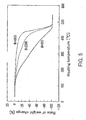
Next, measurements were conducted on changes in weight when
polyethylene with a viscosity-average molecular weight of 900, 2000 or 4000
was heated from a room temperature up to about 550°C in a reduced
pressure atmosphere. The results of the measurements are shown in Fig. 5.
The rate of weight change on the vertical axis indicates how much the
weight decreased as a result of the evaporation of polyethylene as the
temperature rose. As shown in Fig. 5, their rates of weight change all
reach -100% at a certain temperature regardless of their molecular weight.
Thus, it was found that the polyethylene evaporated completely at a certain
temperature. Furthermore, the weight decreased smoothly with increasing
heating temperature. Thus, it was found that polyethylene did not
decompose. When vapor deposition is performed at a temperature higher
than the melting point under a pressure that is not reduced, the
polyethylene generally decomposes, so that the polyethylene serving as the
material and the formed polyethylene film have different properties. On
the other hand, the method of the present invention makes it possible to
form a polyethylene film maintaining the property of the polyethylene
serving as the material. In addition, since the method according to the
present invention forms a film by vapor deposition, a thin polyethylene film
can be formed with excellent controllability.
The invention may be embodied in other specific forms without
departing from the spirit or essential characteristics thereof. The
embodiments disclosed in this application are to be considered in all
respects as illustrative and not restrictive, the scope of the invention being
indicated by the appended claims rather than by the foregoing description,
all changes that come within the meaning and range of equivalency of the
claims are intended to be embraced therein.
As described above, according to the method of the present invention
for manufacturing a resin film, a thin resin film can be formed with
excellent controllability. Also, according to the method of the present
invention for manufacturing an electronic component, an electronic
component including a thin resin film can be manufactured with excellent
controllability.
Claims (10)
- A method for manufacturing a resin film by a vapor deposition of a resin material, the method comprising:depositing the resin material by heating the resin material at a heating temperature higher than a melting point of the resin material in a reduced pressure atmosphere.
- The method according to claim 1, wherein the resin material has a viscosity-average molecular weight ranging from 500 to 1000000.
- The method according to claim 1, wherein the heating temperature is higher than a decomposition temperature of the resin material in an ambient atmosphere and lower than a decomposition temperature of the resin material in the reduced pressure atmosphere.
- The method according to claim 1, wherein the resin material is a polyethylene whose viscosity-average molecular weight ranges from 500 to 10000.
- The method according to claim 4, wherein the heating temperature (°C) is 2.8 to 3.8 times as high as a melting point (°C) of the polyethylene.
- A method for manufacturing an electronic component comprising a resin film formed of a resin material, the method comprising:forming the resin film by a deposition of the resin material by heating the resin material at a heating temperature higher than a melting point of the resin material in a reduced pressure atmosphere.
- The method according to claim 6, wherein the resin material has a viscosity-average molecular weight ranging from 500 to 1000000.
- The method according to claim 7, wherein the heating temperature is higher than a decomposition temperature of the resin material in an ambient atmosphere and lower than a decomposition temperature of the resin material in the reduced pressure atmosphere.
- The method according to claim 7, wherein the resin material is a polyethylene whose viscosity-average molecular weight ranges from 500 to 10000.
- The method according to claim 9, wherein the heating temperature (°C) is 2.8 to 3.8 times as high as a melting point (°C) of the polyethylene.
Applications Claiming Priority (3)
| Application Number | Priority Date | Filing Date | Title |
|---|---|---|---|
| JP2001301248A JP2003105529A (en) | 2001-09-28 | 2001-09-28 | Method of manufacturing resin film, electronic component and method of manufacturing the same |
| JP2001301248 | 2001-09-28 | ||
| PCT/JP2002/009887 WO2003029509A1 (en) | 2001-09-28 | 2002-09-25 | Method for forming resin film and method for manufacturing electronic parts |
Publications (2)
| Publication Number | Publication Date |
|---|---|
| EP1433872A1 true EP1433872A1 (en) | 2004-06-30 |
| EP1433872A4 EP1433872A4 (en) | 2005-02-23 |
Family
ID=19121690
Family Applications (1)
| Application Number | Title | Priority Date | Filing Date |
|---|---|---|---|
| EP02768070A Withdrawn EP1433872A4 (en) | 2001-09-28 | 2002-09-25 | METHOD FOR FORMING RESIN FILM AND METHOD FOR MANUFACTURING ELECTRONIC PARTS |
Country Status (6)
| Country | Link |
|---|---|
| US (1) | US20040039155A1 (en) |
| EP (1) | EP1433872A4 (en) |
| JP (1) | JP2003105529A (en) |
| KR (1) | KR20030077578A (en) |
| CN (1) | CN1494600A (en) |
| WO (1) | WO2003029509A1 (en) |
Families Citing this family (1)
| Publication number | Priority date | Publication date | Assignee | Title |
|---|---|---|---|---|
| CN110218982A (en) * | 2019-07-03 | 2019-09-10 | 唐山中土科技发展有限公司 | A kind of micro-nano resin base film and its processing method |
Family Cites Families (6)
| Publication number | Priority date | Publication date | Assignee | Title |
|---|---|---|---|---|
| GB1298453A (en) * | 1969-01-02 | 1972-12-06 | Nat Res Dev | Production of polymer films by evaporation |
| JPH01119661A (en) * | 1987-10-30 | 1989-05-11 | Sumitomo Electric Ind Ltd | Manufacturing method of organic thin film |
| JPH069918B2 (en) * | 1988-06-02 | 1994-02-09 | セントラル硝子株式会社 | Fluorine-containing resin coated body and method for producing the same |
| JPH07207429A (en) * | 1994-01-14 | 1995-08-08 | Nippon Telegr & Teleph Corp <Ntt> | Water-repellent lubricant material and manufacturing method thereof |
| US6270841B1 (en) * | 1999-07-02 | 2001-08-07 | Sigma Technologies International, Inc. | Thin coating manufactured by vapor deposition of solid oligomers |
| JP2001183503A (en) * | 1999-12-24 | 2001-07-06 | Toray Ind Inc | Optical article manufacturing method |
-
2001
- 2001-09-28 JP JP2001301248A patent/JP2003105529A/en not_active Withdrawn
-
2002
- 2002-09-25 KR KR10-2003-7009448A patent/KR20030077578A/en not_active Ceased
- 2002-09-25 CN CNA028056426A patent/CN1494600A/en active Pending
- 2002-09-25 WO PCT/JP2002/009887 patent/WO2003029509A1/en not_active Ceased
- 2002-09-25 EP EP02768070A patent/EP1433872A4/en not_active Withdrawn
- 2002-09-25 US US10/451,297 patent/US20040039155A1/en not_active Abandoned
Also Published As
| Publication number | Publication date |
|---|---|
| US20040039155A1 (en) | 2004-02-26 |
| WO2003029509A1 (en) | 2003-04-10 |
| EP1433872A4 (en) | 2005-02-23 |
| KR20030077578A (en) | 2003-10-01 |
| JP2003105529A (en) | 2003-04-09 |
| CN1494600A (en) | 2004-05-05 |
Similar Documents
| Publication | Publication Date | Title |
|---|---|---|
| US4345000A (en) | Transparent electrically conductive film | |
| US7947377B2 (en) | Powder mixture to be made into evaporation source material for use in ion plating, evaporation source material for use in ion plating and method of producing the same, and gas barrier sheet and method of producing the same | |
| CN101171360B (en) | Microporous article with metal nanoparticle coating | |
| CA2974791C (en) | Method of manufacturing metal nano coil | |
| US20200163261A1 (en) | Method for manufacturing electromagnetic interference shielding film | |
| JPH05311412A (en) | Vapor deposition material and method for producing transparent barrier film | |
| US6787441B1 (en) | Method for pretreating a polymer substrate using an ion beam for subsequent deposition of indium oxide or indium tin oxide | |
| Paszti et al. | Pressure dependent formation of small Cu and Ag particles during laser ablation | |
| US20070172696A1 (en) | Protective thin film layers and methods of dielectric passivation of organic materials using assisted deposition processes | |
| EP1433872A1 (en) | Method for forming resin film and method for manufacturing electronic parts | |
| US4069356A (en) | Method for rapidly forming photoconductive layers for integrated circuits | |
| CN110230029B (en) | Preparation method of spinel-structured manganese-nickel oxide film | |
| JP2009143759A (en) | Raw material powder of evaporation source material for ion plating, evaporation source material for ion plating and manufacturing method thereof, gas barrier sheet and manufacturing method thereof | |
| KR101922845B1 (en) | The fabricating method of NiTe-based thin film and the conductive substrate fabricated therefor | |
| KR100282024B1 (en) | Method for manufacturing organic electroluminescent device by sputtering | |
| JP2009138248A (en) | Raw material powder of evaporation source material for ion plating, evaporation source material for ion plating and manufacturing method thereof, gas barrier sheet and manufacturing method thereof | |
| KR930005825B1 (en) | Process for producing a transparent polymer film having a electrical conductivity | |
| JPS58157886A (en) | Method for manufacturing phosphor thin film | |
| JP3191320B2 (en) | Plastic coating materials and coated plastic films | |
| KR102680793B1 (en) | Transparent planar heating element and wearable electronic device including the same | |
| JP2623421B2 (en) | Method for producing polymer composite in which fine particles of metal sulfide are dispersed | |
| JP2024143152A (en) | Transparent Conductive Film | |
| JP2025096297A (en) | Transparent Conductive Film | |
| DE102020133316A1 (en) | Process for producing a water-stabilized aluminum oxide layer on a plastic surface | |
| JPH0250950A (en) | Manufacture of vapor-deposited film |
Legal Events
| Date | Code | Title | Description |
|---|---|---|---|
| PUAI | Public reference made under article 153(3) epc to a published international application that has entered the european phase |
Free format text: ORIGINAL CODE: 0009012 |
|
| 17P | Request for examination filed |
Effective date: 20030806 |
|
| AK | Designated contracting states |
Kind code of ref document: A1 Designated state(s): AT BE BG CH CY CZ DE DK EE ES FI FR GB GR IE IT LI LU MC NL PT SE SK TR |
|
| A4 | Supplementary search report drawn up and despatched |
Effective date: 20050112 |
|
| STAA | Information on the status of an ep patent application or granted ep patent |
Free format text: STATUS: THE APPLICATION IS DEEMED TO BE WITHDRAWN |
|
| 18D | Application deemed to be withdrawn |
Effective date: 20050330 |