EP1432118A2 - Oscillation circuit for television tuner - Google Patents
Oscillation circuit for television tuner Download PDFInfo
- Publication number
- EP1432118A2 EP1432118A2 EP03257217A EP03257217A EP1432118A2 EP 1432118 A2 EP1432118 A2 EP 1432118A2 EP 03257217 A EP03257217 A EP 03257217A EP 03257217 A EP03257217 A EP 03257217A EP 1432118 A2 EP1432118 A2 EP 1432118A2
- Authority
- EP
- European Patent Office
- Prior art keywords
- oscillation
- circuit
- transistors
- transistor
- integrated circuit
- Prior art date
- Legal status (The legal status is an assumption and is not a legal conclusion. Google has not performed a legal analysis and makes no representation as to the accuracy of the status listed.)
- Granted
Links
Images
Classifications
-
- H—ELECTRICITY
- H03—ELECTRONIC CIRCUITRY
- H03B—GENERATION OF OSCILLATIONS, DIRECTLY OR BY FREQUENCY-CHANGING, BY CIRCUITS EMPLOYING ACTIVE ELEMENTS WHICH OPERATE IN A NON-SWITCHING MANNER; GENERATION OF NOISE BY SUCH CIRCUITS
- H03B5/00—Generation of oscillations using amplifier with regenerative feedback from output to input
- H03B5/08—Generation of oscillations using amplifier with regenerative feedback from output to input with frequency-determining element comprising lumped inductance and capacitance
- H03B5/12—Generation of oscillations using amplifier with regenerative feedback from output to input with frequency-determining element comprising lumped inductance and capacitance active element in amplifier being semiconductor device
- H03B5/1231—Generation of oscillations using amplifier with regenerative feedback from output to input with frequency-determining element comprising lumped inductance and capacitance active element in amplifier being semiconductor device the amplifier comprising one or more bipolar transistors
-
- H—ELECTRICITY
- H03—ELECTRONIC CIRCUITRY
- H03B—GENERATION OF OSCILLATIONS, DIRECTLY OR BY FREQUENCY-CHANGING, BY CIRCUITS EMPLOYING ACTIVE ELEMENTS WHICH OPERATE IN A NON-SWITCHING MANNER; GENERATION OF NOISE BY SUCH CIRCUITS
- H03B5/00—Generation of oscillations using amplifier with regenerative feedback from output to input
- H03B5/08—Generation of oscillations using amplifier with regenerative feedback from output to input with frequency-determining element comprising lumped inductance and capacitance
- H03B5/12—Generation of oscillations using amplifier with regenerative feedback from output to input with frequency-determining element comprising lumped inductance and capacitance active element in amplifier being semiconductor device
- H03B5/1206—Generation of oscillations using amplifier with regenerative feedback from output to input with frequency-determining element comprising lumped inductance and capacitance active element in amplifier being semiconductor device using multiple transistors for amplification
- H03B5/1212—Generation of oscillations using amplifier with regenerative feedback from output to input with frequency-determining element comprising lumped inductance and capacitance active element in amplifier being semiconductor device using multiple transistors for amplification the amplifier comprising a pair of transistors, wherein an output terminal of each being connected to an input terminal of the other, e.g. a cross coupled pair
- H03B5/1215—Generation of oscillations using amplifier with regenerative feedback from output to input with frequency-determining element comprising lumped inductance and capacitance active element in amplifier being semiconductor device using multiple transistors for amplification the amplifier comprising a pair of transistors, wherein an output terminal of each being connected to an input terminal of the other, e.g. a cross coupled pair the current source or degeneration circuit being in common to both transistors of the pair, e.g. a cross-coupled long-tailed pair
-
- H—ELECTRICITY
- H03—ELECTRONIC CIRCUITRY
- H03B—GENERATION OF OSCILLATIONS, DIRECTLY OR BY FREQUENCY-CHANGING, BY CIRCUITS EMPLOYING ACTIVE ELEMENTS WHICH OPERATE IN A NON-SWITCHING MANNER; GENERATION OF NOISE BY SUCH CIRCUITS
- H03B5/00—Generation of oscillations using amplifier with regenerative feedback from output to input
- H03B5/08—Generation of oscillations using amplifier with regenerative feedback from output to input with frequency-determining element comprising lumped inductance and capacitance
- H03B5/12—Generation of oscillations using amplifier with regenerative feedback from output to input with frequency-determining element comprising lumped inductance and capacitance active element in amplifier being semiconductor device
- H03B5/1237—Generation of oscillations using amplifier with regenerative feedback from output to input with frequency-determining element comprising lumped inductance and capacitance active element in amplifier being semiconductor device comprising means for varying the frequency of the generator
- H03B5/124—Generation of oscillations using amplifier with regenerative feedback from output to input with frequency-determining element comprising lumped inductance and capacitance active element in amplifier being semiconductor device comprising means for varying the frequency of the generator the means comprising a voltage dependent capacitance
- H03B5/1243—Generation of oscillations using amplifier with regenerative feedback from output to input with frequency-determining element comprising lumped inductance and capacitance active element in amplifier being semiconductor device comprising means for varying the frequency of the generator the means comprising a voltage dependent capacitance the means comprising voltage variable capacitance diodes
Definitions
- the invention relates to an oscillation circuit for a television tuner.
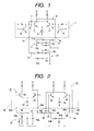
- a conventional oscillation circuit for a television tuner is shown in Fig. 2.
- a first oscillation circuit 31 for a VHF television tuner includes first and second oscillation transistors 32 and 33 formed in an integrated circuit 30, and a first resonance circuit 34 provided outside the integrated circuit 30.
- the first and second oscillation transistors 32 and 33 have their emitters connected with each other and then together to a constant current source 35.
- the second oscillation transistor 33 has its base grounded in terms of high frequencies.
- the integrated circuit 30 is provided with first and second terminals 30a and 30b, and the first oscillation transistor 32 has its base connected to the first terminal 30a and the second oscillation transistor 33 has its collector connected to the second terminal 30b.
- the first resonance circuit 34 includes an inductance element 34a, a varactor diode 34b, and the like, and has one end coupled to the first and second terminals 30a and 30b through two coupling capacitors 36 and 37, respectively.
- the first resonance circuit 34 has its other end grounded.
- a second oscillation circuit 41 for a UHF television tuner includes third and fourth oscillation transistors 42 and 43 provided in the integrated circuit 30 and a second resonance circuit 44 provided outside the integrated circuit 30.
- the third and fourth oscillation transistors 42 and 43 have their emitters connected to each other and then together to a constant current source 45.
- the integrated circuit 30 is provided with third to sixth terminals 30c to 30f.
- the third oscillation transistor 42 has its base connected to the fourth terminal 30d
- the fourth oscillation transistor 43 has its collector connected to the third terminal 30c
- the third oscillation transistor 42 has its collector connected to the sixth terminal 30f
- the fourth oscillation transistor 43 has its base connected to the fifth terminal 30e.
- the second resonance circuit 44 includes an inductance element 44a, and a varactor diode 44b, and has one end coupled to the third and fourth terminals 30c and 30d through two coupling capacitors 46 and 47, respectively.
- the second resonance circuit 44 has its other end connected to the fifth and sixth terminals 30e and 30f through two coupling capacitors 48 and 49, respectively.
- the first oscillation circuit 31 forms an unbalanced oscillation circuit and the second oscillation circuit 41 forms a balanced oscillation circuit.
- An oscillation frequency is set based on tuning voltage applied to the varactor diodes 34b and 44b (see, for example, Patent Document 1).
- the oscillation transistors are used in each of the oscillation circuits. Since these oscillation circuits oscillate at high frequency, the oscillation transistors must have a high transition frequency fT, which raises the cost.
- the transistor of this type has a large chip size and increases the size of an integrated circuit when it is provided in the integrated circuit. The terminals connected to the collectors and bases of the transistors are provided in the integrated circuit, then the resonance circuits are connected to the terminals, and therefore the number of terminals in the integrated circuit increases, which also increases the size of the integrated circuit.
- an oscillation circuit complying first and second oscillation transistors having their emitters connected with each other, and first and second resonance circuits, said first resonance circuit has one end coupled to the base of said first oscillation transistor and the collector of said second oscillation transistor and its other end grounded, said second resonance circuit has one end coupled to the collector of said first oscillation transistor and the base of said second oscillation transistor and its other end grounded, first switch means is connected between one end of said first resonance circuit and ground, second switch means is connected between one end of said second resonance circuit and ground, and said first and second switch means turn on/off reversely from each other.
- said first and second oscillation transistors and said first and second switch transistors are provided in the integrated circuit, said integrated circuit is provided with first and second terminals, the base of said first oscillation transistor and the collector of said second oscillation transistor are coupled to said first terminal through corresponding coupling capacitors provided in said integrated circuit, and the collector of said first oscillation transistor and the base of said second oscillation transistor are coupled to said second terminal through corresponding coupling capacitors provided in said integrated circuit.
- said first and second switch means are each made of a switch transistor, and said first and second switch transistors are provided in said integrated circuit.
- said first and second oscillation transistors and said first resonance circuit form an oscillation circuit for a VHF television tuner
- said first and second oscillation transistors and said second resonance circuit form an oscillation circuit for a UHF television tuner.
- Fig. 1 shows an oscillation circuit for a television tuner according to the invention.
- first and second oscillation transistors 2 and 3 are formed.
- the two oscillation transistors 2 and 3 have their emitters connected with each other and then together to a constant current source 4.
- First and second terminals 1a and 1b are provided in the integrated circuit 1.
- the base of the first oscillation transistor 2 and the collector of the second oscillation transistor 3 are connected to the first terminal 1a through coupling capacitors 5 and 6, respectively provided in the integrated circuit 1.
- the collector of the first oscillation transistor 2 and the base of the second oscillation transistor 3 are connected to the second terminal 1b through coupling capacitors 7 and 8, respectively provided in the integrated circuit 1.
- First and second switch means 9 and 10 are provided in the integrated circuit 1, the first switch means 9 is connected between the first terminal 1a and ground, and the second switch means 10 is connected between the second terminal 1b and ground.
- the first and second switch means 9 and 10 are made of switch transistors, each of which has a collector provided with bias voltage and an emitter grounded. It turns on/off in response to the presence/absence of the bias voltage to the base.
- the switch transistors need only to turn on/off in a DC manner, and therefore may be inexpensive kinds. In this way, the chip size can be reduced.
- First and second resonance circuits 11 and 12 are provided outside the integrated circuit 1.
- the first resonance circuit 11 includes an inductance element 11a, a varactor diode 11b connected in parallel with the inductance element 11a, and the like, and has one end connected to the first terminal 1a through a DC cut capacitor 13 and its other end grounded.
- the varactor diode 11b has its anode grounded in a DC manner.
- the second resonance circuit 12 has an inductance element 12a and a varactor diode 12b connected in series with each other, a varactor diode 12c connected in parallel to the series circuit, and the like.
- the second resonance circuit 12 has one end connected to the second terminal 1b through a DC cut capacitor 14 and its other end grounded.
- the two varactor diodes 12b and 12c have their anodes grounded in a DC manner. Tuning voltage is applied to the cathodes of the three varactor diodes 11b, 12b, and 12c.
- the two switch means 9 and 10 are controlled so that they turn on/off reversely from each other.
- the second switch means 10 When the first switch means 9 is off, the second switch means 10 is on. Consequently, the second resonance circuit 12 has both ends grounded, and the two oscillation transistors 2 and 3, and the first resonance circuit 11 form an unbalanced oscillation circuit.
- the oscillation circuit is used for a VHF tuner.
- the first switch means 9 When the first switch means 9 is on, the second switch means 10 is off. Consequently, the first resonance circuit 11 has both ends grounded, and the two oscillation transistors 2 and 3, and the second resonance circuit 12 form an unbalanced oscillation circuit.
- the oscillation circuit is used for a UHF tuner.
- the two oscillation transistors 2 and 3 are shared by the two resonance circuits 11 and 12, so that the number of the oscillation transistors can be half that of the case when oscillation is caused separately in the two frequency bands.
- the oscillation transistors 2 and 3 have their collectors and bases connected to the first terminals 1a and 1b through the coupling capacitors 5 to 8, so that the number of terminals can be small.
- the first resonance circuit has one end coupled to the base of the first oscillation transistor and the collector of the second oscillation transistor and its other end grounded
- the second resonance circuit has one end coupled to the collector of the first oscillation transistor and the base of the second oscillation transistor and its other end grounded
- the first switch means is connected between one end of the first resonance circuit and ground
- the second switch means is connected between one end of the second resonance circuit and ground
- the first and second switch means turn on/off reversely from each other, so that the two oscillation transistors are shared by the two resonance circuits, and the number of the oscillation transistors can be half the number otherwise necessary when oscillation is caused separately in the two frequency bands. Consequently, the cost can be reduced.
- the first and second oscillation transistors and the first and second switch transistors are provided in the integrated circuit
- the integrated circuit is provided with the first and second terminals
- the base of the first oscillation transistor and the collector of the second oscillation transistor are coupled to the first terminal through the corresponding coupling capacitors provided in the integrated circuit
- the collector of the first oscillation transistor and the base of the second oscillation transistor are coupled to the second terminal through the corresponding coupling capacitors provided in the integrated circuit. Therefore, when the two oscillation transistors 2 and 3 are provided in the integrated circuit 1, the collectors and bases of the oscillation transistors 2 and 3 are connected to the first terminals 1a and 1b through the corresponding coupling capacitors 5 to 8, and the number of terminals canbe reduced. Consequently, the size of the integrated circuit can be reduced.
- first and second switch means are made of switch transistors, and first and second switch transistors are provided in the integrated circuit, so that the size and cost of the integrated circuit can be reduced.
- an oscillation circuit for a VHF television tuner is made of the first and second oscillation transistors and the first resonance circuit
- an oscillation circuit for a UHF television tuner is made of the first and second oscillation transistors and the second resonance circuit. Therefore, the UHF television tuner and the VHF television turner can be provided using the two oscillation transistors.
Landscapes
- Inductance-Capacitance Distribution Constants And Capacitance-Resistance Oscillators (AREA)
- Superheterodyne Receivers (AREA)
Abstract
Description
Claims (4)
- An oscillation circuit for a television tuner, comprising first and second oscillation transistors having their emitters connected with each other, and first and second resonance circuits, wherein said first resonance circuit has one end coupled to the base of said first oscillation transistor and the collector of said second oscillation transistor and its other end grounded, said second resonance circuit has one end coupled to the collector of said first oscillation transistor and the base of said second oscillation transistor and its other end grounded, first switch means is connected between one end of said first resonance circuit and ground, second switch means is connected between one end of said second resonance circuit and ground, and said first and second switch means turn on/off reversely from each other.
- The oscillation circuit for a television tuner according to claim 1, wherein
said first and second oscillation transistors and said first and second switch transistors are provided in the integrated circuit, said integrated circuit is provided with first and second terminals, the base of said first oscillation transistor and the collector of said second oscillation transistor are coupled to said first terminal through corresponding coupling capacitors provided in said integrated circuit, and the collector of said first oscillation transistor and the base of said second oscillation transistor are coupled to said second terminal through corresponding coupling capacitors provided in said integrated circuit. - The oscillation circuit for a television tuner according to claim 1 or 2, wherein
said first and second switch means are each made of a switch transistor, and said first and second switch transistors are provided in said integrated circuit. - The oscillation circuit for a television tuner according to claim 1, 2, or 3, wherein
said first and second oscillation transistors and said first resonance circuit form an oscillation circuit for a VHF television tuner, and said first and second oscillation transistors and said second resonance circuit form an oscillation circuit for a UHF television tuner.
Applications Claiming Priority (2)
| Application Number | Priority Date | Filing Date | Title |
|---|---|---|---|
| JP2002336066 | 2002-11-20 | ||
| JP2002336066A JP2004172933A (en) | 2002-11-20 | 2002-11-20 | Oscillation circuit of television tuner |
Publications (3)
| Publication Number | Publication Date |
|---|---|
| EP1432118A2 true EP1432118A2 (en) | 2004-06-23 |
| EP1432118A3 EP1432118A3 (en) | 2004-07-07 |
| EP1432118B1 EP1432118B1 (en) | 2005-03-30 |
Family
ID=32375734
Family Applications (1)
| Application Number | Title | Priority Date | Filing Date |
|---|---|---|---|
| EP03257217A Expired - Lifetime EP1432118B1 (en) | 2002-11-20 | 2003-11-15 | Oscillation circuit for television tuner |
Country Status (3)
| Country | Link |
|---|---|
| EP (1) | EP1432118B1 (en) |
| JP (1) | JP2004172933A (en) |
| DE (1) | DE60300455T2 (en) |
Family Cites Families (3)
| Publication number | Priority date | Publication date | Assignee | Title |
|---|---|---|---|---|
| JPH11127086A (en) * | 1997-08-19 | 1999-05-11 | Alps Electric Co Ltd | UHF and VHF shared tuner |
| JP3727216B2 (en) * | 2000-03-08 | 2005-12-14 | アルプス電気株式会社 | Television tuner |
| US6593819B2 (en) * | 2001-04-28 | 2003-07-15 | Cts Corporation | Low phase noise dual band voltage controlled oscillator |
-
2002
- 2002-11-20 JP JP2002336066A patent/JP2004172933A/en not_active Withdrawn
-
2003
- 2003-11-15 DE DE60300455T patent/DE60300455T2/en not_active Expired - Lifetime
- 2003-11-15 EP EP03257217A patent/EP1432118B1/en not_active Expired - Lifetime
Also Published As
| Publication number | Publication date |
|---|---|
| EP1432118A3 (en) | 2004-07-07 |
| JP2004172933A (en) | 2004-06-17 |
| DE60300455T2 (en) | 2006-02-23 |
| EP1432118B1 (en) | 2005-03-30 |
| DE60300455D1 (en) | 2005-05-04 |
Similar Documents
| Publication | Publication Date | Title |
|---|---|---|
| JP3930307B2 (en) | Integrated circuit for oscillator | |
| US6226503B1 (en) | Double-tuned circuit | |
| US7139039B2 (en) | Input circuit of television tuner | |
| KR960009970B1 (en) | Tuning device with improved tracking characteristics | |
| US7312672B2 (en) | Local oscillating circuit for receiving high-band and low-band signal | |
| EP1432118B1 (en) | Oscillation circuit for television tuner | |
| EP1432116B1 (en) | Oscillation circuit for television tuner | |
| US7289780B2 (en) | Band switchable type tuning circuit of television signal | |
| US20040183611A1 (en) | Multi-band oscillator that can oscillate at each oscillation band under optimum oscillation conditions | |
| US7349034B2 (en) | Television tuner using integrated circuit | |
| US6307600B1 (en) | Tuning with diode detector | |
| JP3105079U (en) | Oscillation circuit | |
| US20050052579A1 (en) | Television tuner having circuit for attenuating FM broadcasting band | |
| JP3105564U (en) | Television tuner | |
| EP1117177A2 (en) | Voltage controlled oscillator | |
| JP3108419U (en) | Double-tuned circuit | |
| JP3096170U (en) | Television tuner input circuit | |
| EP1263138B1 (en) | Television tuner | |
| JP3977626B2 (en) | Oscillator circuit | |
| JP3101831U (en) | Interstage coupling circuit | |
| JP2002290211A (en) | Band switching dual tuning circuit | |
| JP2002335175A (en) | Television tuner | |
| JP2006086999A (en) | Band-switching tuning circuit | |
| JP2001156592A (en) | Dual tuning circuit | |
| JP2001177379A (en) | Dual-tuning circuit for tuner |
Legal Events
| Date | Code | Title | Description |
|---|---|---|---|
| PUAI | Public reference made under article 153(3) epc to a published international application that has entered the european phase |
Free format text: ORIGINAL CODE: 0009012 |
|
| PUAL | Search report despatched |
Free format text: ORIGINAL CODE: 0009013 |
|
| AK | Designated contracting states |
Kind code of ref document: A2 Designated state(s): AT BE BG CH CY CZ DE DK EE ES FI FR GB GR HU IE IT LI LU MC NL PT RO SE SI SK TR |
|
| AX | Request for extension of the european patent |
Extension state: AL LT LV MK |
|
| AK | Designated contracting states |
Kind code of ref document: A3 Designated state(s): AT BE BG CH CY CZ DE DK EE ES FI FR GB GR HU IE IT LI LU MC NL PT RO SE SI SK TR |
|
| AX | Request for extension of the european patent |
Extension state: AL LT LV MK |
|
| GRAP | Despatch of communication of intention to grant a patent |
Free format text: ORIGINAL CODE: EPIDOSNIGR1 |
|
| 17P | Request for examination filed |
Effective date: 20040823 |
|
| GRAS | Grant fee paid |
Free format text: ORIGINAL CODE: EPIDOSNIGR3 |
|
| GRAA | (expected) grant |
Free format text: ORIGINAL CODE: 0009210 |
|
| AK | Designated contracting states |
Kind code of ref document: B1 Designated state(s): DE FR GB |
|
| AKX | Designation fees paid |
Designated state(s): DE FR GB |
|
| REG | Reference to a national code |
Ref country code: GB Ref legal event code: FG4D |
|
| REF | Corresponds to: |
Ref document number: 60300455 Country of ref document: DE Date of ref document: 20050504 Kind code of ref document: P |
|
| REG | Reference to a national code |
Ref country code: IE Ref legal event code: FG4D |
|
| PLBE | No opposition filed within time limit |
Free format text: ORIGINAL CODE: 0009261 |
|
| STAA | Information on the status of an ep patent application or granted ep patent |
Free format text: STATUS: NO OPPOSITION FILED WITHIN TIME LIMIT |
|
| ET | Fr: translation filed | ||
| 26N | No opposition filed |
Effective date: 20060102 |
|
| PGFP | Annual fee paid to national office [announced via postgrant information from national office to epo] |
Ref country code: DE Payment date: 20091130 Year of fee payment: 7 |
|
| PGFP | Annual fee paid to national office [announced via postgrant information from national office to epo] |
Ref country code: FR Payment date: 20091120 Year of fee payment: 7 Ref country code: GB Payment date: 20091007 Year of fee payment: 7 |
|
| GBPC | Gb: european patent ceased through non-payment of renewal fee |
Effective date: 20101115 |
|
| REG | Reference to a national code |
Ref country code: FR Ref legal event code: ST Effective date: 20110801 |
|
| REG | Reference to a national code |
Ref country code: DE Ref legal event code: R119 Ref document number: 60300455 Country of ref document: DE Effective date: 20110601 Ref country code: DE Ref legal event code: R119 Ref document number: 60300455 Country of ref document: DE Effective date: 20110531 |
|
| PG25 | Lapsed in a contracting state [announced via postgrant information from national office to epo] |
Ref country code: FR Free format text: LAPSE BECAUSE OF NON-PAYMENT OF DUE FEES Effective date: 20101130 |
|
| PG25 | Lapsed in a contracting state [announced via postgrant information from national office to epo] |
Ref country code: GB Free format text: LAPSE BECAUSE OF NON-PAYMENT OF DUE FEES Effective date: 20101115 |
|
| PG25 | Lapsed in a contracting state [announced via postgrant information from national office to epo] |
Ref country code: DE Free format text: LAPSE BECAUSE OF NON-PAYMENT OF DUE FEES Effective date: 20110531 |