EP1431801A2 - Integrated optical apparatus - Google Patents
Integrated optical apparatus Download PDFInfo
- Publication number
- EP1431801A2 EP1431801A2 EP03017115A EP03017115A EP1431801A2 EP 1431801 A2 EP1431801 A2 EP 1431801A2 EP 03017115 A EP03017115 A EP 03017115A EP 03017115 A EP03017115 A EP 03017115A EP 1431801 A2 EP1431801 A2 EP 1431801A2
- Authority
- EP
- European Patent Office
- Prior art keywords
- optical
- inner window
- devices
- integrated
- optical devices
- Prior art date
- Legal status (The legal status is an assumption and is not a legal conclusion. Google has not performed a legal analysis and makes no representation as to the accuracy of the status listed.)
- Withdrawn
Links
Images
Classifications
-
- G—PHYSICS
- G02—OPTICS
- G02B—OPTICAL ELEMENTS, SYSTEMS OR APPARATUS
- G02B6/00—Light guides; Structural details of arrangements comprising light guides and other optical elements, e.g. couplings
- G02B6/10—Light guides; Structural details of arrangements comprising light guides and other optical elements, e.g. couplings of the optical waveguide type
- G02B6/12—Light guides; Structural details of arrangements comprising light guides and other optical elements, e.g. couplings of the optical waveguide type of the integrated circuit kind
-
- G—PHYSICS
- G02—OPTICS
- G02F—OPTICAL DEVICES OR ARRANGEMENTS FOR THE CONTROL OF LIGHT BY MODIFICATION OF THE OPTICAL PROPERTIES OF THE MEDIA OF THE ELEMENTS INVOLVED THEREIN; NON-LINEAR OPTICS; FREQUENCY-CHANGING OF LIGHT; OPTICAL LOGIC ELEMENTS; OPTICAL ANALOGUE/DIGITAL CONVERTERS
- G02F1/00—Devices or arrangements for the control of the intensity, colour, phase, polarisation or direction of light arriving from an independent light source, e.g. switching, gating or modulating; Non-linear optics
- G02F1/01—Devices or arrangements for the control of the intensity, colour, phase, polarisation or direction of light arriving from an independent light source, e.g. switching, gating or modulating; Non-linear optics for the control of the intensity, phase, polarisation or colour
- G02F1/015—Devices or arrangements for the control of the intensity, colour, phase, polarisation or direction of light arriving from an independent light source, e.g. switching, gating or modulating; Non-linear optics for the control of the intensity, phase, polarisation or colour based on semiconductor elements having potential barriers, e.g. having a PN or PIN junction
- G02F1/025—Devices or arrangements for the control of the intensity, colour, phase, polarisation or direction of light arriving from an independent light source, e.g. switching, gating or modulating; Non-linear optics for the control of the intensity, phase, polarisation or colour based on semiconductor elements having potential barriers, e.g. having a PN or PIN junction in an optical waveguide structure
Definitions
- the present invention relates to an integrated optical apparatus including at least two optical devices, more particularly to an integrated optical apparatus, in which electrical and optical insulation is achieved between the optical devices.
- a wave band at 1550 nm of an optical fiber is employed in optical communications in order to transfer ultra high-speed optical signals above 10G bps.
- a distributed-feedback laser diode (DFB LD) coupled to an electro-absorption optical modulator may be used to fabricate an optical transferring system.
- EML electro-absorption modulated laser
- SOA semiconductor optical amplifier
- the electrical insulation and optical insulation between the semiconductor optical amplifier and the electro-absorption optical modulator or the distributed-feedback laser diode are important factors that determine performance capacities of the integrated devices.
- One embodiment of the present invention is directed to an integrated optical apparatus including: at least two optical devices each equipped with an optical waveguide, and inner windows interposed at regions including the optical waveguides between the optical devices.
- the inner windows disconnect the optical waveguides that are located between the optical devices in order to achieve optical/electrical insulation.
- the optical insulation between the optical devices can be controlled by the length of the inner window.
- the inner window may be filled with a semiconductor material after removing the optical waveguides.
- the inner window may be filled with an air layer after removing the optical waveguides.
- the electrical insulation between the optical devices can be controlled by the electrical conductivity of the material constituting the inner window.
- the material used to form the inner window is a semiconductor, and the electrical conductivity can be controlled by the doping concentration of a dopant.
- the optical devices include a laser diode and a semiconductor optical amplifier, and the optically insulated inner window is formed between the laser diode and the semiconductor optical amplifier.
- the laser diode may be a distributed feedback laser diode integrated with an electro-absorption optical modulator.
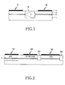
- FIG. 1 is a diagram illustrating principles of optical insulation for an integrated optical apparatus according to aspects of the present invention.
- an integrated optical apparatus includes a first optical device 10, a second optical device 20 and an inner window 30 interposed between the first and second.
- a plurality of material layers forms the optical devices 10 and 20.
- the material layers are formed on a substrate 1 and have a structure that commonly includes an optical waveguide 2.
- the optical waveguide 2 is preferably covered with a cladding layer 3.
- Element 4 in Fig. 1 represents an electrode. Since these material layers should be known to one of ordinary skill in the art, a detailed description of the constituting material layers of the optical devices 10 and 20 is omitted.
- the inner window 30 is interposed at a portion removed of the optical waveguide 2 between the optical devices 10 and 20 and the inner window 30 insulates the optical devices 10 and 20 optically and electrically.
- the electrical insulation is achieved through controlling the electric conductivity of the materials constituting the inner window 30.
- the doping concentration of the dopant In the case of semiconductor material, it is practically controlled through controlling the doping concentration of the dopant.
- optical waveguiding principles it is noted that an optical mode present in an inner part of a semiconductor device is confined by the optical waveguide produced from differences of refractive indices.
- the optical confinement thus produced enables the activation of the semiconductor device.
- the optical confinement enables the lasers to oscillate, and in the case of the optical modulators, it enables them to absorb light in order to produce modulated signals.
- semiconductor optical amplifiers it enables the increase of optical amplifying efficiency.
- the technical principle of the inner window 30 is to remove the common optical waveguide 2 between the two devices 10 and 20.
- the inner window 30 can be constituted in various ways, as described below.
- the optical waveguide 2 between the two devices 10and 20 can simply be removed.
- a portion where the optical waveguide has been removed is filled with air.
- the optical waveguide 2 between the two devices 10 and 20 is removed, and the portion where the optical waveguide has been removed is filled with some material.
- the semiconductor device it can be substantially filled by regrowing a lower layer of the semiconductor device.
- FIG. 2 is a diagram showing an example of an integrated optical apparatus according to a preferred embodiment of the present invention.
- the integrated optical apparatus includes a distributed-feedback laser diode (DFB LD) 100, an electro-absorption optical modulator (EA-Modulator) 200, a semiconductor optical amplifier (SOA) 300 and two inner windows 250 and 350.
- the above three devices all include optical waveguides 2, and the inner windows 250 and 350 are interposed between the devices requiring the optical/electrical insulations after the optical waveguides 2 have been removed.
- Detailed description of the material layers constituting the optical devices 100, 200 and 300 as already referred to with regard to FIG. 1 has been omitted for clarity.
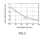
- the coupling efficiency i.e., the amounts of the optical insulation, can be controlled by a length of the inner windows 250 and 350.
- FIG 3 is a chart showing calculated results of coupling efficiency (dB) according to an inner window length of the present invention and the coupling efficiency (E) obtained from the actual manufactured device shown in FIG. 2. As apparent from FIG. 3, optical insulation reaching 15 dB can be produced between the two integrated optical devices.
- An integrated optical apparatus can be obtained by removing the optical waveguides between the respective optical devices at the time of integrating optical devices having independent characteristics, and interposing the inner windows there between to achieve optical/electrical insulations.
Landscapes
- Physics & Mathematics (AREA)
- Nonlinear Science (AREA)
- General Physics & Mathematics (AREA)
- Optics & Photonics (AREA)
- Engineering & Computer Science (AREA)
- Microelectronics & Electronic Packaging (AREA)
- Semiconductor Lasers (AREA)
- Optical Modulation, Optical Deflection, Nonlinear Optics, Optical Demodulation, Optical Logic Elements (AREA)
- Optical Integrated Circuits (AREA)
Abstract
Description
junction with the accompanying drawings, in which:
Claims (17)
- An integrated optical apparatus comprising:at least two optical devices, each of which includes an optical waveguide; andat least one inner window interposed between the optical devices to form a gap between the optical waveguides of the at least two optical devices.
- The integrated optical apparatus as claimed in claim 1, wherein the at least one inner window functions to achieve optical/electrical insulation between the at least two optical devices.
- The integrated optical apparatus as claimed in claim 2, wherein the optical insulation between the at least two optical devices can be controlled by a length of the at least one inner window.
- The integrated optical apparatus as claimed in claim 1 or 2, wherein the inner window is filled with a semiconductor material.
- The integrated optical apparatus as claimed in one of claims 1 to 4, wherein the inner window is filled with air.
- The integrated optical apparatus as claimed in claim 2 or 3, wherein the electrical insulation between the at least two optical devices can be controlled by an electric conductivity of a material constituting the at least one inner window.
- The integrated optical apparatus as claimed in claim 2 or 6, wherein the material constituting the inner window is a semiconductor, and the electric conductivity can be controlled by a doping concentration of a dopant of the semiconductor.
- The integrated optical apparatus as claimed in one of claims 1 to 7, wherein the at least two optical devices are a laser diode and a semiconductor optical amplifier, and the at least one inner window is formed between the laser diode and the semiconductor optical amplifier.
- The integrated optical apparatus as claimed in claim 8, wherein the laser diode is a distributed feedback laser diode integrated with an electro-absorption optical modulator.
- A method of forming an integrated optical apparatus comprising the step of:forming at least two optical devices, each including a common optical waveguide; andremoving a portion of the common optical waveguide that is located between the at least two optical devices, wherein the removed portion forms an inner window that functions to achieve optical/electrical insulation between the at least two optical devices.
- The method as claimed in claim 10, further comprising the step of adjusting the optical insulation between the at least two optical devices by controlled by a length of the removed portion.
- The method as claimed in claim 10 or 11, further comprising the step of filling the inner window with a semiconductor material.
- The method as claimed in claim 10 or 11, further comprising the step of filling the inner window with air.
- The method as claimed in one of claims 10 to 12, further comprising the step of adjusting the electrical insulation between the at least two optical devices by controlling by an electric conductivity of the semiconductor material used to fill the inner window.
- The method as claimed in claim 14, wherein the electric conductivity is controlled by a doping concentration of a dopant of the semiconductor material.
- The method as claimed in one of claims 10 to 15, wherein the at least two optical devices are a laser diode and a semiconductor optical amplifier, and the inner window is formed between the laser diode and the semiconductor optical amplifier.
- The method as claimed in claim 16, wherein the laser diode is a distributed feedback laser diode integrated with an electro-absorption optical modulator.
Applications Claiming Priority (2)
| Application Number | Priority Date | Filing Date | Title |
|---|---|---|---|
| KR2002080665 | 2002-12-17 | ||
| KR10-2002-0080665A KR100493089B1 (en) | 2002-12-17 | 2002-12-17 | Integrated optical device |
Publications (2)
| Publication Number | Publication Date |
|---|---|
| EP1431801A2 true EP1431801A2 (en) | 2004-06-23 |
| EP1431801A3 EP1431801A3 (en) | 2005-06-29 |
Family
ID=32388331
Family Applications (1)
| Application Number | Title | Priority Date | Filing Date |
|---|---|---|---|
| EP03017115A Withdrawn EP1431801A3 (en) | 2002-12-17 | 2003-07-28 | Integrated optical apparatus |
Country Status (4)
| Country | Link |
|---|---|
| US (1) | US20040114871A1 (en) |
| EP (1) | EP1431801A3 (en) |
| JP (1) | JP2004200697A (en) |
| KR (1) | KR100493089B1 (en) |
Cited By (1)
| Publication number | Priority date | Publication date | Assignee | Title |
|---|---|---|---|---|
| US11726262B2 (en) | 2019-11-18 | 2023-08-15 | Danmarks Tekniske Universitet | In-plane chip-scale photonic device |
Families Citing this family (1)
| Publication number | Priority date | Publication date | Assignee | Title |
|---|---|---|---|---|
| WO2007080891A1 (en) * | 2006-01-11 | 2007-07-19 | Nec Corporation | Semiconductor laser, module, and optical transmitter |
Family Cites Families (16)
| Publication number | Priority date | Publication date | Assignee | Title |
|---|---|---|---|---|
| GB1543405A (en) * | 1975-03-29 | 1979-04-04 | Licentia Gmbh | Method of and arrangement for producing coherent mode radiation |
| US4503541A (en) * | 1982-11-10 | 1985-03-05 | The United States Of America As Represented By The Secretary Of The Navy | Controlled-linewidth laser source |
| JPS61160987A (en) * | 1985-01-09 | 1986-07-21 | Nec Corp | Integrated semiconductor photo element and manufacture thereof |
| JPH041614A (en) * | 1990-04-18 | 1992-01-07 | Mitsubishi Electric Corp | Optical amplifying device |
| US5103455A (en) * | 1990-05-09 | 1992-04-07 | Gte Laboratories Incorporated | Monolithically integrated semiconductor optical preamplifier |
| JP2980435B2 (en) * | 1991-09-12 | 1999-11-22 | 株式会社東芝 | Semiconductor device |
| US5548607A (en) * | 1994-06-08 | 1996-08-20 | Lucent Technologies, Inc. | Article comprising an integrated laser/modulator combination |
| FR2737354B1 (en) * | 1995-07-26 | 1997-08-22 | France Telecom | INTEGRATED MONOLITHIC LASER-MODULATOR-AMPLIFIER COMPONENT WITH QUANTUM MULTI-WELL STRUCTURE |
| JPH0964334A (en) * | 1995-08-28 | 1997-03-07 | Toshiba Corp | Integrated device of light emitting device and external modulator |
| DE19624514C1 (en) * | 1996-06-19 | 1997-07-17 | Siemens Ag | Monolithically integrated semiconductor laser-modulator combination |
| KR100424774B1 (en) * | 1998-07-22 | 2004-05-17 | 삼성전자주식회사 | Mask for forming selection area diffraction grating and growing selection area and method of manufacturing semiconductor device using the same |
| SE9902916L (en) * | 1999-08-16 | 2001-02-17 | Ericsson Telefon Ab L M | Modulator and integrated circuit |
| US6928223B2 (en) * | 2000-07-14 | 2005-08-09 | Massachusetts Institute Of Technology | Stab-coupled optical waveguide laser and amplifier |
| US6459716B1 (en) * | 2001-02-01 | 2002-10-01 | Nova Crystals, Inc. | Integrated surface-emitting laser and modulator device |
| US6803604B2 (en) * | 2001-03-13 | 2004-10-12 | Ricoh Company, Ltd. | Semiconductor optical modulator, an optical amplifier and an integrated semiconductor light-emitting device |
| US6526083B1 (en) * | 2001-10-09 | 2003-02-25 | Xerox Corporation | Two section blue laser diode with reduced output power droop |
-
2002
- 2002-12-17 KR KR10-2002-0080665A patent/KR100493089B1/en not_active Expired - Fee Related
-
2003
- 2003-06-17 US US10/464,130 patent/US20040114871A1/en not_active Abandoned
- 2003-07-28 EP EP03017115A patent/EP1431801A3/en not_active Withdrawn
- 2003-12-17 JP JP2003419758A patent/JP2004200697A/en active Pending
Cited By (1)
| Publication number | Priority date | Publication date | Assignee | Title |
|---|---|---|---|---|
| US11726262B2 (en) | 2019-11-18 | 2023-08-15 | Danmarks Tekniske Universitet | In-plane chip-scale photonic device |
Also Published As
| Publication number | Publication date |
|---|---|
| KR100493089B1 (en) | 2005-06-02 |
| US20040114871A1 (en) | 2004-06-17 |
| KR20040052437A (en) | 2004-06-23 |
| JP2004200697A (en) | 2004-07-15 |
| EP1431801A3 (en) | 2005-06-29 |
Similar Documents
| Publication | Publication Date | Title |
|---|---|---|
| JP3323725B2 (en) | Polarization modulation laser, driving method thereof, and optical communication system using the same | |
| US8363314B2 (en) | Reflective semiconductor optical amplifier (R-SOA) and superluminescent diode (SLD) | |
| US9728938B2 (en) | Optical semiconductor device, optical semiconductor device array, and optical transmitter module | |
| JP5545847B2 (en) | Optical semiconductor device | |
| JPWO2006077641A1 (en) | Optical waveguide device and semiconductor device | |
| JP2019008179A (en) | Semiconductor optical device | |
| JP2019054107A (en) | Semiconductor optical device | |
| JP3284994B2 (en) | Semiconductor optical integrated device and method of manufacturing the same | |
| JP2005352219A (en) | Semiconductor electro-absorption type optical modulator, semiconductor electro-absorption type optical modulator integrated laser, optical transmitting module and optical transmitting receiving module | |
| JP4006159B2 (en) | Semiconductor electroabsorption optical modulator integrated light emitting device, light emitting device module, and optical transmission system | |
| JP3674806B2 (en) | Semiconductor optical waveguide functional element | |
| JP6320192B2 (en) | Wavelength variable light source and wavelength variable light source module | |
| JP2011258785A (en) | Optical waveguide and optical semiconductor device using it | |
| CN112956091A (en) | Anti-reflection laser | |
| JP2016149529A (en) | Wavelength-tunable light source and wavelength-tunable light source module | |
| EP1130708B1 (en) | Semiconductor electro-absorption optical modulator integrated light emitting element and module, and optical transmission system | |
| EP1431801A2 (en) | Integrated optical apparatus | |
| JP7680690B2 (en) | Optical Modulator and Transmitter | |
| JPH09289354A (en) | Semiconductor laser device and optical coupling device | |
| JP2002116419A (en) | Light modulation device and method of manufacturing the same | |
| JPH1073791A (en) | Semiconductor Mach-Zehnder type optical modulator, optical modulator module and optical transmission device | |
| WO2023233525A1 (en) | Optical transmitter | |
| KR100249812B1 (en) | Butte-Coupled DifferBee Laser and Optical Modulator Integrated Device and Manufacturing Method Thereof | |
| JPWO2005060058A1 (en) | Semiconductor laser and manufacturing method thereof | |
| Matsuo | High-performance lasers on InP-SOI platform |
Legal Events
| Date | Code | Title | Description |
|---|---|---|---|
| PUAI | Public reference made under article 153(3) epc to a published international application that has entered the european phase |
Free format text: ORIGINAL CODE: 0009012 |
|
| 17P | Request for examination filed |
Effective date: 20030728 |
|
| AK | Designated contracting states |
Kind code of ref document: A2 Designated state(s): AT BE BG CH CY CZ DE DK EE ES FI FR GB GR HU IE IT LI LU MC NL PT RO SE SI SK TR |
|
| AX | Request for extension of the european patent |
Extension state: AL LT LV MK |
|
| PUAL | Search report despatched |
Free format text: ORIGINAL CODE: 0009013 |
|
| AK | Designated contracting states |
Kind code of ref document: A3 Designated state(s): AT BE BG CH CY CZ DE DK EE ES FI FR GB GR HU IE IT LI LU MC NL PT RO SE SI SK TR |
|
| AX | Request for extension of the european patent |
Extension state: AL LT LV MK |
|
| RIC1 | Information provided on ipc code assigned before grant |
Ipc: 7H 01S 5/026 B Ipc: 7G 02F 1/025 A |
|
| STAA | Information on the status of an ep patent application or granted ep patent |
Free format text: STATUS: THE APPLICATION HAS BEEN WITHDRAWN |
|
| AKX | Designation fees paid |
Designated state(s): DE FR GB |
|
| 18W | Application withdrawn |
Effective date: 20060213 |