EP1429353A1 - Push-button switch-use member and production method therefor - Google Patents
Push-button switch-use member and production method therefor Download PDFInfo
- Publication number
- EP1429353A1 EP1429353A1 EP02763004A EP02763004A EP1429353A1 EP 1429353 A1 EP1429353 A1 EP 1429353A1 EP 02763004 A EP02763004 A EP 02763004A EP 02763004 A EP02763004 A EP 02763004A EP 1429353 A1 EP1429353 A1 EP 1429353A1
- Authority
- EP
- European Patent Office
- Prior art keywords
- metal member
- holes
- push
- metal
- button switch
- Prior art date
- Legal status (The legal status is an assumption and is not a legal conclusion. Google has not performed a legal analysis and makes no representation as to the accuracy of the status listed.)
- Granted
Links
Images


Classifications
-
- H—ELECTRICITY
- H01—ELECTRIC ELEMENTS
- H01H—ELECTRIC SWITCHES; RELAYS; SELECTORS; EMERGENCY PROTECTIVE DEVICES
- H01H1/00—Contacts
- H01H1/06—Contacts characterised by the shape or structure of the contact-making surface, e.g. grooved
-
- H—ELECTRICITY
- H01—ELECTRIC ELEMENTS
- H01H—ELECTRIC SWITCHES; RELAYS; SELECTORS; EMERGENCY PROTECTIVE DEVICES
- H01H13/00—Switches having rectilinearly-movable operating part or parts adapted for pushing or pulling in one direction only, e.g. push-button switch
- H01H13/70—Switches having rectilinearly-movable operating part or parts adapted for pushing or pulling in one direction only, e.g. push-button switch having a plurality of operating members associated with different sets of contacts, e.g. keyboard
- H01H13/78—Switches having rectilinearly-movable operating part or parts adapted for pushing or pulling in one direction only, e.g. push-button switch having a plurality of operating members associated with different sets of contacts, e.g. keyboard characterised by the contacts or the contact sites
- H01H13/785—Switches having rectilinearly-movable operating part or parts adapted for pushing or pulling in one direction only, e.g. push-button switch having a plurality of operating members associated with different sets of contacts, e.g. keyboard characterised by the contacts or the contact sites characterised by the material of the contacts, e.g. conductive polymers
-
- H—ELECTRICITY
- H01—ELECTRIC ELEMENTS
- H01H—ELECTRIC SWITCHES; RELAYS; SELECTORS; EMERGENCY PROTECTIVE DEVICES
- H01H1/00—Contacts
- H01H1/06—Contacts characterised by the shape or structure of the contact-making surface, e.g. grooved
- H01H1/10—Laminated contacts with divided contact surface
-
- H—ELECTRICITY
- H01—ELECTRIC ELEMENTS
- H01H—ELECTRIC SWITCHES; RELAYS; SELECTORS; EMERGENCY PROTECTIVE DEVICES
- H01H2201/00—Contacts
-
- H—ELECTRICITY
- H01—ELECTRIC ELEMENTS
- H01H—ELECTRIC SWITCHES; RELAYS; SELECTORS; EMERGENCY PROTECTIVE DEVICES
- H01H2201/00—Contacts
- H01H2201/022—Material
- H01H2201/03—Composite
Definitions
- the present invention relates to a member for a push-button switch provided with a metal member contacting an opposing electrode, and more specifically, to a member for a push-button switch and manufacturing method of the same hardly causing a conductive fault even in the presence of a fine insulating foreign material between the push-button switch member and the opposing electrode.
- a plate-shaped metal member is used as a member for the push-button switch (hereafter merely called a push-button switch member).
- a plate-shaped metal member is used as the push-button switch member.
- Fig. 7 is a schematic partial sectional view showing a push-button switch capable of withstanding such a high current.
- reference numeral 1 denotes a contact structure composed of a plate-shaped metal
- a keypad 2 is formed of a resin such as silicone rubber which is operatively pushed from an external side
- the contact structure 1 is integrally formed to the keypad 2 in a manner opposing to an opposing electrode 4 of a stationary substrate 3 so as to be capable of being contacted to the contact structure 1, thus constituting a movable contact.
- a metal plate which is formed by gold-plating a German silver metal sheet and then punched out therefrom in a predetermined shape.
- a current passes through the contacting of such metal plate having good conductive performance to the opposing electrode 4, high current can be conducted, and moreover, since the metal plate has a strength strong enough to substantially prevent the contact structure 1 from being damaged or broken by a repeated pushing or pressing operation given to a push-button B, and hence, enough to provide desired durability.
- the metal plate has a strength too high to deform the same. Accordingly, as shown in Fig. 8, if fine foreign material 5 such as dirt or dust having an insulating property intrudes into the switch and adheres to a portion between the contact structure 1 and the opposing electrode 4, it is difficult for the metal plate to be deformed in accordance with the shape of the fine foreign material 5 at a time when the contact structure 1 contacts the opposing electrode 4, which will adversely result in formation of a wide gap 5a therebetween, largely reducing a contacting area and, hence, causing defective conduction of the push-button switch, thus causing problems.
- fine foreign material 5 such as dirt or dust having an insulating property intrudes into the switch and adheres to a portion between the contact structure 1 and the opposing electrode 4
- the present invention therefore provides a member for a push-button switch positively preventing reduction of a contacting area of a contact structure and an opposing electrode both constituting a movable contact even if insulating foreign material exists between the contact structure and the opposing electrode and providing an improved durability, and also provides a manufacturing method capable of easily manufacturing such push-button switch member.
- the first aspect provides a member for a push-button switch having a movable contact made of a metal member consisting of a contact surface to be contacted to an opposing electrode, in which a number of holes are formed to the contact surface so as to extend in a height direction thereof and the holes are filled up with a filler formed of flexible resin.
- the insulating foreign material having a size smaller than the sectional area of the hole, to intrude into the holes, so that the contacting area between the opposing electrode and the end portion of the metal wall of the metal member surrounding the hole constituting the contact surface is not reduced.
- the metal member can easily be deformed because of the formation of number of holes, so that the metal member can be locally deformed in accordance with the insulating foreign material, and the contacting area is thus not reduced so largely. Therefore, even in the presence of the insulating foreign material having a size smaller than the sectional area of the hole between the push-button switch member and the opposing electrode, sufficient contacting area can be ensured, thus hardly causing conductive fault or conduction problems.
- the metal wall surrounding each of the holes oriented in a height (depth) direction thereof has a solid structure, so that the metal member can provide a desired strength as a whole, thus ensuring the durability.
- the wall section between the adjacent holes can be reinforced by the filler, and in addition, since the filler is formed of flexible resin, the local deformation of the metal member cannot be adversely obstructed. Therefore, even if the metal member has a thin wall it can hardly be broken by the repeated local deforming force, thus improving the durability.
- the second aspect is characterized, in addition to the first aspect , in that the filler is filled up in the full height direction of the metal member.
- the end portion of the filler provides a same flat surface as that of the end portion of the metal wall and the metal wall can be entirely reinforced by the filler, so that excellent durability can be provided. Moreover, even if the insulating foreign material intrudes into the holes, the insulating foreign material can be easily separated from the holes, at the time when the push-button switch member is separated apart from the opposing electrode, by the elastic recovering force of the end portion of the filler, so that the repeated use in normal condition can always be ensured.
- the third aspect is characterized, in addition to the first and second aspects , in that the metal member has a honeycomb shape densed structure formed with a number of through holes having same sectional shape.
- the strength in the full height direction of the metal member can be made higher, and the metal wall between the adjacent through holes can also be made thinner, so that the flexibility of the end portion of the metal wall can be further improved while maintaining the improved durability.
- the fourth aspect is a method of manufacturing a member for a push-button switch provided with a movable. contact composed of a metal member constituting a contact surface to an opposing electrode, which is characterized by comprising the steps of forming a number of through holes to the metal member so as to penetrate in a height direction thereof, arranging a filler formed of a flexible resin sheet on one end surface side of the metal member, forming a metal member base material in which the through holes are filled up with the filler by the full height amount by pressurizing the metal member in the height direction thereof, punching out the metal member base material so as to provide a contact structure having a predetermined shape, and joining the contact structure to a keypad.
- the metal member which is made deformable by the formation of a number of through holes is reinforced by the filler, so that the deformation of the metal member in the punching-out step or steps thereafter can be prevented and the degree of flatness of the contact surface in the manufacturing process cannot be damaged. Accordingly, the member for the push-button switch can easily be manufactured.
- a contact structure of a push-button switch member according to the embodiment of the present invention is shown in Figs. 1 and 2. Further, it is to be noted that a state that this contact structure is applied to a keypad is identical to that shown in Fig. 8.
- Fig. 1 is a plan view of a metal member of the contact structure.
- Fig. 2 is a vertical view of an essential portion of the contact structure of the push-button switch member.
- This contact structure 1 is provided with a metal member 7 having a dense structure of substantially honeycomb shape formed with a plurality of through holes 6, which have the same sectional shape, penetrating in a height (depth) direction thereof and also provided with a filler 8 formed of flexible resin such as silicone rubber filling the through holes 6 of the metal member 7 from the side of a keypad 2.
- the filler 8 is arranged so that one end portion 8a of the filler 8 has substantially the same plane of one end portion 7a, in the height direction, of the metal member 7, and there exists no filler 8 on the outer surface of the end portion 7a, thus constituting a contact surface to the opposing electrode 4.
- the honeycomb-shaped dense structure of the metal member 7 indicates a structure, as shown in Fig. 3, in which a plurality of mutually adjacent through holes 6 are formed close to each other through metal walls 7c having equal height smaller than the height of the metal member 7. That is, it is not always necessary for the through hole 6 to have the same sectional shape of hexagon as that of the honeycomb structure, and it may be possible to have other polygonal shape such as triangular, pentagonal or octagonal shape, or even to have a circular shape.
- the metal walls 7c, each constituting a boundary between the adjacent two through holes 6, are all continuous, and in order to provide the metal walls 7c having even thickness, the sectional shape of the through hole 6 may be selected from triangualar, quadrangular or hexagonal shape.
- the contact structure mentioned above even in the case where the insulating foreign material 5 such as dust or dirt intruding into the switch member exists between the opposing electrode 4 and the push-button switch member 1, since a plurality of through holes 6 are formed to the end portion 7a of the metal member 7, the insulating foreign material 5 intrudes into the through holes 6 or the metal member 7 is locally deformed in accordance with the insulating foreign material 5 to thereby suppress the reduction of the contacting area, thus being difficult to cause a defective conduction.
- the insulating foreign material 5 such as dust or dirt intruding into the switch member exists between the opposing electrode 4 and the push-button switch member 1
- the metal walls 7c provide a solid structure by a plurality of through holes 6 oriented in the height direction, so that it is possible to sufficiently ensure the entire strength of the metal member 7, thus preventing the degradation of the durability of the contact structure.
- the structure can be reinforced by the filler 8 even if the metal wall 7c is formed to be thin, and moreover, since this filler 8 is formed of a flexible resin material, it is permitted for the metal member to be locally deformed.
- the thin metal wall 7c can be subjected to the repeated local deformation and the durability: of the structure can hence be ensured.
- the filler 8 of the filling amount satisfying at least more than 1/2 height of the metal member 7, and specifically, by filling up to the full height of the through hole 6 so that the end portion 8a of the filler 8 reaches to the same plane as the end portion 7a of the metal wall 7c, all the metal walls 7c are reinforced by the filler 8, so that the further improved durability is obtainable.
- the insulating foreign material 5 can easily be removed from the through hole 6, at the time of separation of the contact structure 1 from the opposing electrode 4, due to the elastic restoring force of the end portion 8a of the filler 8, so that the contact structure can repeatedly be used always in the stable condition.
- the metal member 7 has approximately a honeycomb-shaped dense structure, the metal member 7 can provide high mechanical strength in its height direction, and at any portion of the end portion 7a of the metal member 7, it is possible to make the thickness of the metal walls 7c thinner, thus making the contact surface more flexible while suitably maintaining the durability.
- the metal member 7 is formed from a sheet member formed with a number of through holes 6, and accordingly, the end portion 7a, constituting the contacting surface, of the metal wall 7c of the metal member 7 is formed to provide a plane shape, so that it is possible to make the contacting area larger in comparison with a structure in which a member such as metal mesh, which is formed by knitting warp and weft wires or the like each having a diameter substantially identical to the thickness of the metal wall 7c, contacts at points separated from each other, and in addition, the pressure on the contacting surface and the stress applied to the metal wall 7c are made uniform, so that the structure provides less fatigue even during repeated use and the suitable durability can be maintained.
- a member such as metal mesh which is formed by knitting warp and weft wires or the like each having a diameter substantially identical to the thickness of the metal wall 7c
- the metal member 7 is formed with the through holes 6 penetrating in the height direction thereof, it is not always necessary for the through holes 6 to penetrate the same in the height direction as far as the metal member 7 is formed, at least at its contact surface, with holes extending in the height direction of the metal member 7 from the contact surface.
- the material 5 invades into the hole formed to the contact surface of the metal member 7, so that the contacting area between the end portion 7a of the metal member 7 and the opposing electrode 4 is never reduced, and hence, the conductive performance is never deteriorated.
- a number of through holes 6, which penetrate a metal sheet in its height direction, are formed to the metal sheet through, for example, an etching treatment to thereby obtain a metal sheet 11 having a dense structure in the form of a honeycomb structure.
- the metal sheet 11 is then subjected to a primer treatment, and as shown in Fig. 6b, a filler sheet 12 made of silicone rubber is laminated on one side surface of the metal sheet 11. Thereafter, such filler sheet 12 is pressurized in the height direction by means of a predetermined mold and then heated so as to provide an integrated structure. According to such process, as shown in Fig.
- a base material H of the metal body is produced in which a number of through holes 6 are filled up with the filler in their full height direction.
- the filler 8 remains on one side surface of the metal body base material H, but it does not exist on the other side surface thereof.
- the thus formed metal sheet is punched out in a predetermined shape to thereby obtain the contact structure 1 such as shown in Fig. 1.
- the filler 8 and the keypad 2 provide the same material, and therefore, a member P for the push-button switch in which these materials are integrated can be completed easily.
- the filler sheet 12 is arranged to the metal sheet 11 having a number of through holes 6 formed so as to penetrate in the height direction, which is then pressurized in the height direction, it is easy to fill the through holes 6 with the filler 8.
- the metal sheet 11 is punched out so as to provide a predetermined shape with the through holes 6 being filled up with the filler 8, so that the metal member 7, which is easily deformable because of the formation of a number of through holes 6, can be reinforced by the filler 8, and the metal member 7 can be prevented from being deformed at the punch-out process of the metal sheet or joining process to the keypad 2. Accordingly, the degree of flatness of the end portion 7a constituting the contact surface will easily be maintained, thus being easy to manufacture the member P for the push-button switch.
- a metal sheet 11 having a densed structure, in which a number of through holes 6, each having a hexagonal shape, are arranged so as to provide a honeycomb structure was manufactured by performing an etching treatment to a metal sheet formed of SUS304 having a thickness of 50 ⁇ m.
- the end portions 7a, 7b of the metal wall 7c had a thickness (line width, hereinlater) of 20 ⁇ m, a width between the parallel metal walls 7c, 7c (space width, hereinlater) was 185 ⁇ m, the sectional area of the through hole 6 (hole area, hereinlater) was 29640 ⁇ m 2 , the hole area/metallic portion area of metal member (opening, hereinlater) was 81.4%, and the filling rate (100 minus opening) was 18.6%.
- the primer treatment was then effected in a manner such that a primer No.18 (manufactured by Shin-Etsu Chemical Co., Ltd. ) was coated on one side of the metal sheet having a dense structure in the form of a honeycomb shape by using a brush, which was then dried for one hour in an environment of a temperature of 200°C.
- a primer No.18 manufactured by Shin-Etsu Chemical Co., Ltd.
- a laminated body was obtained by bonding, to this primer treatment surface, a filler sheet 12, which was prepared by a silicone rubber (which was prepared by mixing silicone compound KE-951U of 100 parts by weight, manufactured by Shin-Etsu Chemical Co., Ltd. and a cross-linking agent C-8 of 2 parts by weight, manufactured by Shin-Etsu Chemical Co., Ltd.) and having a height of 1.0 mm.
- a filler sheet 12 which was prepared by a silicone rubber (which was prepared by mixing silicone compound KE-951U of 100 parts by weight, manufactured by Shin-Etsu Chemical Co., Ltd. and a cross-linking agent C-8 of 2 parts by weight, manufactured by Shin-Etsu Chemical Co., Ltd.) and having a height of 1.0 mm.
- this laminated body was placed in a predetermined mold and then formed under compression at a temperature of 160°C and a pressure of 180kg/cm 2 for 5 minutes, thus obtaining a product in the shape of a sheet in which a number of through holes 6 were filled up with silicone rubber in their full height direction.
- the thus obtained product was then punched out so as to provide a predetermined shape to thereby obtain the contact structure 1.
- the thus obtained contact structure 1 was placed in the mold for formation of the predetermined keypad with the surface covered by the silicone rubber being directed upward, and a silicone rubber sheet, which was formed of a silicone rubber (which was prepared bymixing silicone compound KE-941U of 100 parts by weight, manufactured by Shin-Etsu Chemical Co . , Ltd. a cross-linking agent C-8 of 2 parts by weight, manufactured by Shin-Etsu Chemical Co., Ltd.) and having a height of 2.0 mm, which was then formed under compression at a temperature of 175°C and a pressure of 200kg/cm 2 for 5 minutes, thus obtaining a member P for push-button switch composed of an integrated body of the contact structure 1 and the keypad 2.
- a silicone rubber sheet which was formed of a silicone rubber (which was prepared bymixing silicone compound KE-941U of 100 parts by weight, manufactured by Shin-Etsu Chemical Co . , Ltd. a cross-linking agent C-8 of 2 parts by weight, manufactured by Shin-Etsu
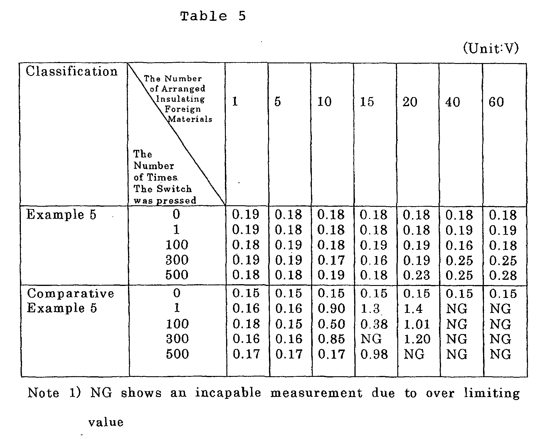
- the thus manufactured member P for the push-button switch was applied to the push-button switch such as shown in Fig. 1, and a predetermined number of insulating foreign materials 5, each being substantially spherical and having a particle diameter of 50 ⁇ m, were distributed almost evenly on the opposing electrode 4. In this state, the electrical characteristics were measured for carrying out a conduction test.
- a member for the push-button switch was manufactured by substantially the same conditions as those in the Example 1 except that the through holes 6 were not formed to the metal sheet 11 and the same conduction test as that of the Example 1 was performed. The test result is shown in Table 1.
- the same conduction test was performed by using the same contact structure as that in the Example 1 except that there was used a metal sheet 11 composed of SUS304, having a height of 50 ⁇ m, having a dense structure in the form of substantially a honeycomb shape having the line width of 45 ⁇ m, the space width of 380 ⁇ m, the hole area of 125054 ⁇ m 2 and the opening of 79.9%, and the silicone rubber has a filling rate of 20.1% and except that the insulating foreign materials 5, each being substantially spherical and having a particle diameter of 200 ⁇ m, were used.
- the test result is shown in Table 3.
- the line width was of 60 ⁇ m
- the space width was of 100um
- hole area was of 8660 ⁇ m 2
- the opening was of 39.1%.
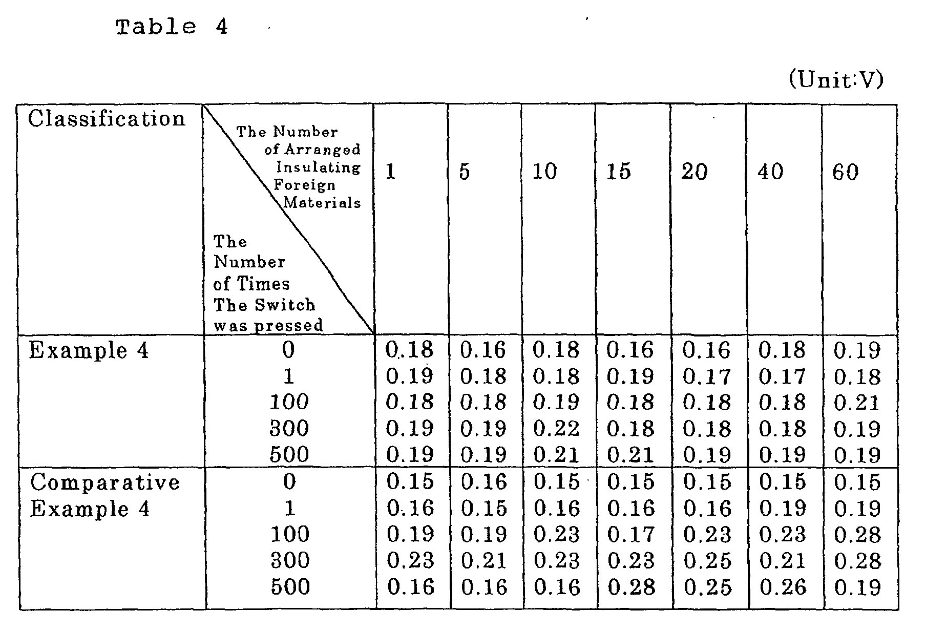
- Gold plating was effected to the entire surface of the thus manufactured metal sheet 11 so as to provide a plated thickness of 0.5 ⁇ m, and thereafter, the contact structure was prepared with the same conditions as those in the Example 1 and a conduction test was then performed with the same conditions as those of the Example 1. Test result is shown in Table 4.
- the contact structure was manufactured with the same conditions as those in the Example 4 except that no through hole was formed to the metal sheet. Test result is shown in Table 4.
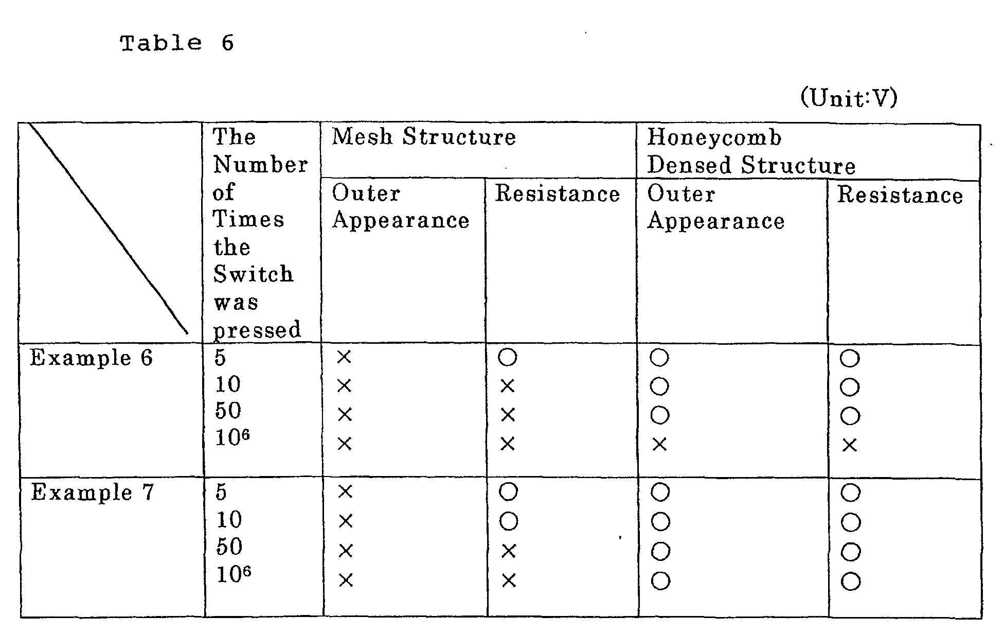
- contact structures 1 each formed of material of SUS304, having the line width of 20 ⁇ m, the space width of 185 ⁇ m and the hole area of 29640 ⁇ m 2 and using a dense honeycomb structure and a mesh structure (line diameter of 20 ⁇ m) by the same method as in the Example 1.
- Push-button switch members were prepared by using such contact structures 1, and outer appearance and resistance thereof, after pressing them with load of 200g and with no current load, were compared.
- the evaluation of the outer appearance was made by visually observing the contacting surface and one having injury or defect was considered to be bad (X) .
- the evaluation of the resistance was made by observing sparks which was generated at the time of lowering of the insulating resistance between two patterns on the stationary substrates 3 and when the spark was observed, it was considered to be bad or defective (X). The results are shown in Table 6.
- the contact structure utilizing the honeycomb- shaped dense structure provided the excellent durability as compared with the contact structure utilizing the mesh structure.
- the contact structure of the mesh structure has, on its contact surface, a number of recessed portions penetrating in the height direction, advantageous effect to foreign materials could be expected as well as the contact structure of the honeycomb -shaped structure.
- the vertical and horizontal wires of the mesh structure is inferior in durability, this is not available for the use requiring the durability though being applicable to the push-button switch which does not require the durability so much.
- the contact structure in the case of the honeycomb-shaped dense structure could provide the usable durability as far as it has the line width of 20 ⁇ m.
- a push-button switch member hardly causing a conductive fault even in the presence of a fine insulating foreign material. It could therefore be preferably utilized as a push-button switch member, such as one utilized for a power window, door mirror or the like, having a contact to which high electric current passes or one having a normally closed type contact for which it is required to prevent a sticking phenomenon.
Landscapes
- Push-Button Switches (AREA)
- Manufacture Of Switches (AREA)
- Contacts (AREA)
Abstract
Description


Claims (4)
- A member for a push-button switch having a movable contact made of a metal member comprising a contact surface to be contacted to an opposing electrode, wherein a number of holes are formed to the contact surface so as to extend in a height direction thereof and the holes are filled up with a filler formed of flexible resin.
- A member for a push-button switch according to claim 1, wherein said through holes are filled up with the filler in a full height direction of the metal member.
- A member for a push-button switch according to claim 1 or 2, wherein said metal member has a honeycomb-shaped dense structure formed with a number of through holes having the same sectional shape.
- A method of manufacturing a member for a push-button switch provided with a movable contact composed of a metal member constituting a contact surface to an opposing electrode, comprising the steps of forming a number of through holes to the metal member so as to penetrate in a height direction thereof, arranging a filler formed of a flexible resin sheet on one end surface side of the metal member, forming a metal member base material in which the through holes are filled up with the filler in the full height direction amount by pressurizing the metal member in the height direction thereof, punching out the metal member base material so as to provide a contact structure having a predetermined shape, and joining the contact structure to a keypad.
Applications Claiming Priority (3)
| Application Number | Priority Date | Filing Date | Title |
|---|---|---|---|
| JP2001289892 | 2001-09-21 | ||
| JP2001289892 | 2001-09-21 | ||
| PCT/JP2002/008980 WO2003028054A1 (en) | 2001-09-21 | 2002-09-04 | Push-button switch-use member and production method therefor |
Publications (3)
| Publication Number | Publication Date |
|---|---|
| EP1429353A1 true EP1429353A1 (en) | 2004-06-16 |
| EP1429353A4 EP1429353A4 (en) | 2007-01-10 |
| EP1429353B1 EP1429353B1 (en) | 2011-11-16 |
Family
ID=19112322
Family Applications (1)
| Application Number | Title | Priority Date | Filing Date |
|---|---|---|---|
| EP02763004A Expired - Lifetime EP1429353B1 (en) | 2001-09-21 | 2002-09-04 | Push-button switch-use member and production method therefor |
Country Status (6)
| Country | Link |
|---|---|
| US (1) | US6870116B2 (en) |
| EP (1) | EP1429353B1 (en) |
| JP (1) | JP4044043B2 (en) |
| KR (1) | KR100886278B1 (en) |
| CN (1) | CN100452260C (en) |
| WO (1) | WO2003028054A1 (en) |
Cited By (1)
| Publication number | Priority date | Publication date | Assignee | Title |
|---|---|---|---|---|
| EP2378530A4 (en) * | 2009-01-15 | 2013-12-25 | Covac Co Ltd | Metal mesh contact and switch and method for procuding the same |
Families Citing this family (5)
| Publication number | Priority date | Publication date | Assignee | Title |
|---|---|---|---|---|
| JP2005174788A (en) * | 2003-12-12 | 2005-06-30 | Matsushita Electric Ind Co Ltd | Push-on switch |
| JP2006296497A (en) * | 2005-04-15 | 2006-11-02 | Olympus Corp | Endoscope apparatus |
| US7832628B2 (en) * | 2005-10-21 | 2010-11-16 | Verifone, Inc. | Protective cover for terminal keypad security switches |
| KR102051782B1 (en) * | 2019-07-04 | 2020-01-08 | 박세홍 | Silicon contacts and silicon contacts manufacturing Method |
| CN115172094B (en) * | 2022-06-30 | 2025-12-23 | Abb瑞士股份有限公司 | Vacuum interrupter post and related electrical equipment |
Family Cites Families (10)
| Publication number | Priority date | Publication date | Assignee | Title |
|---|---|---|---|---|
| US3562466A (en) * | 1969-09-02 | 1971-02-09 | Gen Electric | Make-and-break composite electrical contacts |
| US3654407A (en) * | 1970-06-08 | 1972-04-04 | Sylvania Electric Prod | Compression switch |
| JPS5795020U (en) * | 1980-12-02 | 1982-06-11 | ||
| JPS5795020A (en) * | 1980-12-03 | 1982-06-12 | Alps Electric Co Ltd | Switching substrate and method of producing same |
| JPH0412417A (en) * | 1990-04-27 | 1992-01-17 | Seiko Epson Corp | Switch substrate |
| JPH10144168A (en) | 1996-11-12 | 1998-05-29 | Sensor Technol Kk | Planar switch |
| LU90200B1 (en) * | 1998-01-21 | 1999-07-22 | Iee Sarl | Switching element in foil construction |
| JP2000173375A (en) * | 1998-12-07 | 2000-06-23 | Omron Corp | Contact structure for micro relay |
| JP2000222977A (en) * | 1999-02-02 | 2000-08-11 | Funai Electric Co Ltd | Key switch structure |
| JP4442963B2 (en) * | 1999-10-26 | 2010-03-31 | パナソニック株式会社 | Button switch |
-
2002
- 2002-09-04 EP EP02763004A patent/EP1429353B1/en not_active Expired - Lifetime
- 2002-09-04 CN CNB028133668A patent/CN100452260C/en not_active Expired - Lifetime
- 2002-09-04 WO PCT/JP2002/008980 patent/WO2003028054A1/en not_active Ceased
- 2002-09-04 US US10/484,448 patent/US6870116B2/en not_active Expired - Lifetime
- 2002-09-04 JP JP2003531488A patent/JP4044043B2/en not_active Expired - Lifetime
- 2002-09-04 KR KR1020037016470A patent/KR100886278B1/en not_active Expired - Lifetime
Cited By (2)
| Publication number | Priority date | Publication date | Assignee | Title |
|---|---|---|---|---|
| EP2378530A4 (en) * | 2009-01-15 | 2013-12-25 | Covac Co Ltd | Metal mesh contact and switch and method for procuding the same |
| US8686307B2 (en) | 2009-01-15 | 2014-04-01 | Covac Co., Ltd. | Metal mesh contact and switch and method for producing the same |
Also Published As
| Publication number | Publication date |
|---|---|
| CN100452260C (en) | 2009-01-14 |
| JPWO2003028054A1 (en) | 2005-01-13 |
| KR100886278B1 (en) | 2009-03-04 |
| US20040168898A1 (en) | 2004-09-02 |
| WO2003028054A1 (en) | 2003-04-03 |
| CN1531737A (en) | 2004-09-22 |
| HK1069673A1 (en) | 2005-05-27 |
| US6870116B2 (en) | 2005-03-22 |
| JP4044043B2 (en) | 2008-02-06 |
| EP1429353B1 (en) | 2011-11-16 |
| EP1429353A4 (en) | 2007-01-10 |
| KR20040032112A (en) | 2004-04-14 |
Similar Documents
| Publication | Publication Date | Title |
|---|---|---|
| TWI547043B (en) | Test socket | |
| EP2434859B1 (en) | Conductive contact terminal to be mounted on a substrate surface | |
| KR20140089391A (en) | Electroactive polymer transducers | |
| US8686307B2 (en) | Metal mesh contact and switch and method for producing the same | |
| EP1429353B1 (en) | Push-button switch-use member and production method therefor | |
| US20020115356A1 (en) | Graded metallic leads for connection to microelectronic elements | |
| KR20190037621A (en) | Conductive contact and anisotropic conductive sheet with the same | |
| US20050146414A1 (en) | Connecting unit including contactor having superior electrical conductivity and resilience, and method for producing the same | |
| WO2014092173A1 (en) | Rivet contact and method for manufacturing same | |
| JP6255089B2 (en) | Structure for heat transfer interface and method of manufacturing the same | |
| JP4003208B2 (en) | Elastic electrical contact | |
| TWI542086B (en) | Anisotropic conductive connector, manufacturing and device thereof | |
| US20260104437A1 (en) | Probe for probe card | |
| JP3951333B2 (en) | Anisotropic conductive rubber sheet and manufacturing method thereof | |
| HK1069673B (en) | Push-button switch member and method of manufacturing same | |
| JP6657051B2 (en) | Contact member and member for push button switch including the same | |
| KR102766869B1 (en) | Test socket | |
| CN212848070U (en) | Burr-resistant metal and rubber composite electric contact | |
| JP4712255B2 (en) | Contact member for pushbutton switch | |
| JP2011039066A (en) | Multilayer electric probe and method of manufacturing the same | |
| US20190287739A1 (en) | Contact member, contact member production method, and push-button switch member equipped with contact member | |
| CN214043448U (en) | Rubber and metal composite electric contact without glue overflow | |
| CN109494084B (en) | Conductive part for switch, button switch and conductive part manufacturing method | |
| KR200400380Y1 (en) | Key pad for electronic device | |
| JP2003123868A (en) | Conductive rubber sheet and manufacturing method of the same, and pressure contact connector |
Legal Events
| Date | Code | Title | Description |
|---|---|---|---|
| PUAI | Public reference made under article 153(3) epc to a published international application that has entered the european phase |
Free format text: ORIGINAL CODE: 0009012 |
|
| 17P | Request for examination filed |
Effective date: 20040225 |
|
| AK | Designated contracting states |
Kind code of ref document: A1 Designated state(s): AT BE BG CH CY CZ DE DK EE ES FI FR GB GR IE IT LI LU MC NL PT SE SK TR |
|
| AX | Request for extension of the european patent |
Extension state: AL LT LV MK RO SI |
|
| A4 | Supplementary search report drawn up and despatched |
Effective date: 20061208 |
|
| RIC1 | Information provided on ipc code assigned before grant |
Ipc: H01H 1/10 20060101AFI20061204BHEP |
|
| 17Q | First examination report despatched |
Effective date: 20091026 |
|
| GRAP | Despatch of communication of intention to grant a patent |
Free format text: ORIGINAL CODE: EPIDOSNIGR1 |
|
| RBV | Designated contracting states (corrected) |
Designated state(s): DE FR GB IT SE |
|
| GRAS | Grant fee paid |
Free format text: ORIGINAL CODE: EPIDOSNIGR3 |
|
| GRAA | (expected) grant |
Free format text: ORIGINAL CODE: 0009210 |
|
| AK | Designated contracting states |
Kind code of ref document: B1 Designated state(s): DE FR GB IT SE |
|
| REG | Reference to a national code |
Ref country code: GB Ref legal event code: FG4D |
|
| REG | Reference to a national code |
Ref country code: DE Ref legal event code: R096 Ref document number: 60241572 Country of ref document: DE Effective date: 20120126 |
|
| PG25 | Lapsed in a contracting state [announced via postgrant information from national office to epo] |
Ref country code: SE Free format text: LAPSE BECAUSE OF FAILURE TO SUBMIT A TRANSLATION OF THE DESCRIPTION OR TO PAY THE FEE WITHIN THE PRESCRIBED TIME-LIMIT Effective date: 20111116 |
|
| REG | Reference to a national code |
Ref country code: DE Ref legal event code: R082 Ref document number: 60241572 Country of ref document: DE Representative=s name: STORK BAMBERGER PATENTANWAELTE, DE Ref country code: DE Ref legal event code: R082 Ref document number: 60241572 Country of ref document: DE Representative=s name: STORK BAMBERGER PATENTANWAELTE PARTMBB, DE |
|
| PG25 | Lapsed in a contracting state [announced via postgrant information from national office to epo] |
Ref country code: IT Free format text: LAPSE BECAUSE OF FAILURE TO SUBMIT A TRANSLATION OF THE DESCRIPTION OR TO PAY THE FEE WITHIN THE PRESCRIBED TIME-LIMIT Effective date: 20111116 |
|
| PLBE | No opposition filed within time limit |
Free format text: ORIGINAL CODE: 0009261 |
|
| STAA | Information on the status of an ep patent application or granted ep patent |
Free format text: STATUS: NO OPPOSITION FILED WITHIN TIME LIMIT |
|
| 26N | No opposition filed |
Effective date: 20120817 |
|
| REG | Reference to a national code |
Ref country code: DE Ref legal event code: R097 Ref document number: 60241572 Country of ref document: DE Effective date: 20120817 |
|
| REG | Reference to a national code |
Ref country code: FR Ref legal event code: PLFP Year of fee payment: 15 |
|
| REG | Reference to a national code |
Ref country code: FR Ref legal event code: PLFP Year of fee payment: 16 |
|
| REG | Reference to a national code |
Ref country code: FR Ref legal event code: PLFP Year of fee payment: 17 |
|
| PGFP | Annual fee paid to national office [announced via postgrant information from national office to epo] |
Ref country code: FR Payment date: 20210921 Year of fee payment: 20 |
|
| PGFP | Annual fee paid to national office [announced via postgrant information from national office to epo] |
Ref country code: GB Payment date: 20210920 Year of fee payment: 20 Ref country code: DE Payment date: 20210920 Year of fee payment: 20 |
|
| REG | Reference to a national code |
Ref country code: DE Ref legal event code: R071 Ref document number: 60241572 Country of ref document: DE |
|
| REG | Reference to a national code |
Ref country code: GB Ref legal event code: PE20 Expiry date: 20220903 |
|
| PG25 | Lapsed in a contracting state [announced via postgrant information from national office to epo] |
Ref country code: GB Free format text: LAPSE BECAUSE OF EXPIRATION OF PROTECTION Effective date: 20220903 |