EP1429170A1 - Optical switch and optical switch array - Google Patents
Optical switch and optical switch array Download PDFInfo
- Publication number
- EP1429170A1 EP1429170A1 EP02767979A EP02767979A EP1429170A1 EP 1429170 A1 EP1429170 A1 EP 1429170A1 EP 02767979 A EP02767979 A EP 02767979A EP 02767979 A EP02767979 A EP 02767979A EP 1429170 A1 EP1429170 A1 EP 1429170A1
- Authority
- EP
- European Patent Office
- Prior art keywords
- movable member
- mirror
- optical switch
- switch according
- electrode
- Prior art date
- Legal status (The legal status is an assumption and is not a legal conclusion. Google has not performed a legal analysis and makes no representation as to the accuracy of the status listed.)
- Granted
Links
Images






Classifications
-
- G—PHYSICS
- G02—OPTICS
- G02B—OPTICAL ELEMENTS, SYSTEMS OR APPARATUS
- G02B26/00—Optical devices or arrangements for the control of light using movable or deformable optical elements
- G02B26/08—Optical devices or arrangements for the control of light using movable or deformable optical elements for controlling the direction of light
-
- G—PHYSICS
- G02—OPTICS
- G02B—OPTICAL ELEMENTS, SYSTEMS OR APPARATUS
- G02B6/00—Light guides; Structural details of arrangements comprising light guides and other optical elements, e.g. couplings
- G02B6/24—Coupling light guides
- G02B6/26—Optical coupling means
- G02B6/35—Optical coupling means having switching means
- G02B6/351—Optical coupling means having switching means involving stationary waveguides with moving interposed optical elements
- G02B6/3512—Optical coupling means having switching means involving stationary waveguides with moving interposed optical elements the optical element being reflective, e.g. mirror
- G02B6/3514—Optical coupling means having switching means involving stationary waveguides with moving interposed optical elements the optical element being reflective, e.g. mirror the reflective optical element moving along a line so as to translate into and out of the beam path, i.e. across the beam path
-
- G—PHYSICS
- G02—OPTICS
- G02B—OPTICAL ELEMENTS, SYSTEMS OR APPARATUS
- G02B6/00—Light guides; Structural details of arrangements comprising light guides and other optical elements, e.g. couplings
- G02B6/10—Light guides; Structural details of arrangements comprising light guides and other optical elements, e.g. couplings of the optical waveguide type
- G02B6/12—Light guides; Structural details of arrangements comprising light guides and other optical elements, e.g. couplings of the optical waveguide type of the integrated circuit kind
- G02B6/122—Basic optical elements, e.g. light-guiding paths
-
- G—PHYSICS
- G02—OPTICS
- G02B—OPTICAL ELEMENTS, SYSTEMS OR APPARATUS
- G02B6/00—Light guides; Structural details of arrangements comprising light guides and other optical elements, e.g. couplings
- G02B6/10—Light guides; Structural details of arrangements comprising light guides and other optical elements, e.g. couplings of the optical waveguide type
- G02B6/12—Light guides; Structural details of arrangements comprising light guides and other optical elements, e.g. couplings of the optical waveguide type of the integrated circuit kind
- G02B2006/12083—Constructional arrangements
- G02B2006/12104—Mirror; Reflectors or the like
-
- G—PHYSICS
- G02—OPTICS
- G02B—OPTICAL ELEMENTS, SYSTEMS OR APPARATUS
- G02B6/00—Light guides; Structural details of arrangements comprising light guides and other optical elements, e.g. couplings
- G02B6/24—Coupling light guides
- G02B6/26—Optical coupling means
- G02B6/35—Optical coupling means having switching means
- G02B6/351—Optical coupling means having switching means involving stationary waveguides with moving interposed optical elements
- G02B6/3512—Optical coupling means having switching means involving stationary waveguides with moving interposed optical elements the optical element being reflective, e.g. mirror
- G02B6/3518—Optical coupling means having switching means involving stationary waveguides with moving interposed optical elements the optical element being reflective, e.g. mirror the reflective optical element being an intrinsic part of a MEMS device, i.e. fabricated together with the MEMS device
-
- G—PHYSICS
- G02—OPTICS
- G02B—OPTICAL ELEMENTS, SYSTEMS OR APPARATUS
- G02B6/00—Light guides; Structural details of arrangements comprising light guides and other optical elements, e.g. couplings
- G02B6/24—Coupling light guides
- G02B6/26—Optical coupling means
- G02B6/35—Optical coupling means having switching means
- G02B6/3564—Mechanical details of the actuation mechanism associated with the moving element or mounting mechanism details
- G02B6/3566—Mechanical details of the actuation mechanism associated with the moving element or mounting mechanism details involving bending a beam, e.g. with cantilever
-
- G—PHYSICS
- G02—OPTICS
- G02B—OPTICAL ELEMENTS, SYSTEMS OR APPARATUS
- G02B6/00—Light guides; Structural details of arrangements comprising light guides and other optical elements, e.g. couplings
- G02B6/24—Coupling light guides
- G02B6/26—Optical coupling means
- G02B6/35—Optical coupling means having switching means
- G02B6/3564—Mechanical details of the actuation mechanism associated with the moving element or mounting mechanism details
- G02B6/3568—Mechanical details of the actuation mechanism associated with the moving element or mounting mechanism details characterised by the actuating force
- G02B6/357—Electrostatic force
-
- G—PHYSICS
- G02—OPTICS
- G02B—OPTICAL ELEMENTS, SYSTEMS OR APPARATUS
- G02B6/00—Light guides; Structural details of arrangements comprising light guides and other optical elements, e.g. couplings
- G02B6/24—Coupling light guides
- G02B6/26—Optical coupling means
- G02B6/35—Optical coupling means having switching means
- G02B6/3564—Mechanical details of the actuation mechanism associated with the moving element or mounting mechanism details
- G02B6/3584—Mechanical details of the actuation mechanism associated with the moving element or mounting mechanism details constructional details of an associated actuator having a MEMS construction, i.e. constructed using semiconductor technology such as etching
-
- G—PHYSICS
- G02—OPTICS
- G02B—OPTICAL ELEMENTS, SYSTEMS OR APPARATUS
- G02B6/00—Light guides; Structural details of arrangements comprising light guides and other optical elements, e.g. couplings
- G02B6/24—Coupling light guides
- G02B6/26—Optical coupling means
- G02B6/35—Optical coupling means having switching means
- G02B6/3596—With planar waveguide arrangement, i.e. in a substrate, regardless if actuating mechanism is outside the substrate
Definitions
- the present invention relates to an optical switch and optical switch array used in optical communication and the like.
- a conventionally known optical switch is described in, e.g., "Vertical Mirrors Fabricated by Deep Reactive Ion Etching for Fiber-Optic Switching Applications", J. Microelectromechanical System Vol. 6, 1997, p. 277 - p. 285.
- the optical switch described in this reference switches by inserting and retracting a mirror attached to the end of a support arm into and from an optical path by using an electrostatic actuator.
- An optical switch of the present invention is characterized by comprising a base member, a planar waveguide formed on the base member, a movable member cantilevered by the base member wherein a position of its distal end portion in a plane of the planar waveguide is movable by deformation of the movable member, a mirror fixed to the distal end portion of the movable member, and driving means for switching a light propagation direction in the planar waveguide by deforming the movable member and changing the mirror position with respect to the planar waveguide.
- the mirror for changing the optical path is disposed at the distal end of the movable member, and the mirror position can be switched by deformation of the movable member. Accordingly, since the switching mirror position on a plane of planar waveguide is achieved not by the moving of the displacement of moving member but by deformation of moving member, the size of the optical switch can be decreased. This achieves downsizing and high integration of the optical switch. As a consequence, an optical switch array can be easily formed.
- the driving means comprises a main electrode opposing the movable member, and means for generating electrostatic force between the main electrode and the movable member.
- the movable member is attracted to the main electrode with the proximal end of the movable member as a center, by the electrostatic force generated between the main electrode and movable member. Accordingly, the mirror moves in the direction substantially perpendicular to the extending direction of the movable member.
- the driving means can be implemented with a simple arrangement.
- the spacing between the main electrode and the movable member decreases from the distal end to the proximal end of the electrode.
- the spacing between the main electrode and movable member decreases as a whole as the movable member approaches the main electrode. This increases the electrostatic force generated between the main electrode and movable member. Therefore, it is possible to lower the driving force (driving voltage) of the movable member and decrease the length of this movable member.
- the movable member comprises a first comb having a plurality of teeth, and a second comb having a plurality of teeth to be inserted between the teeth of the first comb is formed in that portion of the electrode, which opposes the first comb. Since the surface area of the main electrode increases, the electrostatic force generated between this main electrode and the movable member also increases. Accordingly, it is possible to lower the driving force (driving voltage) of the movable member and decrease the length of this movable member.
- a comb supporting portion is formed at the end portion of the movable member, and the first comb is formed on the comb supporting portion.
- the electrostatic force generated between the main electrode and movable member concentrates to the end portion of the movable member, and so the displacement amount of the end portion of the movable member also increases. This makes it possible to further decrease the driving force of the movable member and move the mirror efficiently.
- the lengths of the teeth of the second comb can be made different from each other such that the spacing between the distal end of each tooth of the first comb and the proximal end of each tooth of the second comb increases from the proximal end to the distal end of the main electrode.
- the spacing between the distal end of each tooth of the first comb and the proximal end of each tooth of the second comb decreases as a whole, and this increases the electrostatic force generated between them. Therefore, it is possible to further lower the driving voltage of the movable member and further decrease the length of this movable member.
- the driving means favorably further comprises a returning electrode placed on the side of the movable member away from the main electrode, and means for generating electrostatic force between the returning electrode and the movable member.
- a returning electrode placed on the side of the movable member away from the main electrode
- means for generating electrostatic force between the returning electrode and the movable member When, with the movable member attracted to the main electrode, the electrostatic force between the main electrode and movable member is turned off and at the same time electrostatic force is generated between the returning electrode and movable member, the movable member is attracted to the returning electrode by this electrostatic force, and the mirror returns to its initial position. This raises the driving speed of the movable member when the mirror is returned, compared to the case in which the mirror is returned to the initial position only by the biasing force of the movable member.
- the optical switch favorably further comprises position holding means for holding the mirror in a first position at which the mirror intercepts light propagating on the optical path and a second position at which the mirror passes light propagating on the optical path.
- position holding means for holding the mirror in a first position at which the mirror intercepts light propagating on the optical path and a second position at which the mirror passes light propagating on the optical path.
- the position holding means preferably comprises a position holding movable portion placed in front of the mirror and having a first projection for holding the mirror in the first position and a second projection for holding the mirror in the second position, a position holding driving portion for moving the position holding movable portion in the extending direction of the movable member, and a holding recess which is formed in the end portion of the movable member and into which the first and second projections are inserted.
- the position holding movable portion is moved toward the movable member to fit the first projection into the holding recess.
- the position holding movable portion is moved toward the movable member to fit the second projection into the holding recess.
- the position holding movable portion is moved away from the movable member. Consequently, the mirror can be reliably held in the first or second position.
- the position holding means can be a spring member which is placed in front of the mirror, is in contact with the end portion of the movable member, and has spring force which biases the movable member.
- the mirror is held in the first or second position as the movable member is pushed by the spring member.
- driving force larger than the spring force of the spring member is generated in the movable member by the driving means, thereby contracting the spring member. Consequently, the mirror can be reliably held in the first or second position.
- the structure of the position holding means is simplified because no actuator is necessary.
- the position holding means can comprise a position holding movable portion placed in front of the mirror, a position holding electrode opposing the position holding movable portion, a first holding notch formed in the end portion of the movable member to lock the position holding movable portion such that the mirror is held in the first position, and a second holding notch formed in the end portion of the movable member to lock the position holding movable portion such that the mirror is held in the second position.
- the position holding movable portion is moved away from the position holding electrode and locked in the first holding notch.
- the position holding movable portion is moved away from the position holding electrode and locked in the second holding notch.
- the position holding movable portion is moved toward the position holding electrode. Accordingly, the mirror can be reliably held in the first or second position.
- the movable member is designed such that the mirror intercepts light propagating on the optical path in a normal state.
- the mirror surface is parallel to the widthwise direction of the switch. As a consequence, light is reflected by the mirror without any deterioration of the optical characteristics.
- the planar waveguide can comprise a cladding removed portion formed by removing the cladding except for a portion around the core, and a cut portion which is formed on the optical path to connect to the cladding removed portion, and into which the mirror enters, and the movable member can be formed in the cladding removed portion such that the mirror is positioned in the same plane as the core. Since the height of the optical switch can be decreased, a 1 x 2 optical switch, for example, can be downsized.
- the cladding removed portion is preferably formed by removing the cladding by reactive ion etching.
- the cladding can be readily removed to leave any arbitrary shape.
- the movable member and the mirror are simultaneously formed using the same material. This simplifies the formation steps of the movable member and mirror.
- the movable member and the mirror are preferably made of silicon, since a mirror having appropriate reflectivity can be easily formed.
- a mirror device comprising the movable member and the mirror is bonded to the planar waveguide. This facilitates the manufacture of the optical switch.
- an aligning projection is formed on one of the planar waveguide and the mirror device, and an aligning recess which fits on this aligning projection is formed in the other of the planar waveguide and the mirror device.
- planar waveguide and the mirror device are preferably bonded by anodic bonding. Since an adhesive or the like need not be used in the bonding, deformation by temperature can be prevented. Consequently, the planar waveguide and mirror device can be stably bonded.
- a substrate of this planar waveguide is favorably made of silicon or glass containing alkali metal ion. This facilitates the anodic bonding.
- An optical switch array of the present invention is fixing a plurality of optical switches described above on the same base member.
- the array pitch of the mirror devices is 500 ⁇ m or less. Accordingly, a smaller and more highly integrated optical switch array can be obtained.
- Fig. 1 is a schematic view showing the second embodiment of the optical switch according to the present invention.
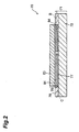
- Fig. 2 is a sectional view taken along a line II - II in Fig. 1.
- an optical switch 70 of this embodiment is a 1 ⁇ 2 switch.
- This optical switch 70 has a planar waveguide 71 having a substrate 72 made of silicon or glass such as silica glass or soda glass containing alkali metal ion.
- An optical waveguide 76 is formed on this substrate 72.
- This optical waveguide 76 includes a core 91 forming optical paths A to C and a cladding 92 formed around the core 91 (see Figs. 2A and 2B).
- the substrate 72 also has cladding removed portions 73 formed by removing the cladding 92 except for portions around the core 91.
- a cut portion 74 connecting to the cladding removed portions 73 is formed in the upper surface of a central portion of this substrate 72.
- the optical paths A to C cross each other in this cut portion 74.
- the distance between the optical paths A and B is, e.g., 250 ⁇ m.
- the width of the cut portion 74 is, e.g., 50 ⁇ m.
- aligning projections 90 are formed on the substrate 72.
- a mirror device 75 is mounted on the upper surface of this base substrate 72.
- This mirror device 75 has a silicon substrate 83 on which (on the lower surface of the silicon substrate 83) a movable member 77 and electrode 80 are formed via a 2- ⁇ m thick insulating layer 84 made of silicon dioxide (SiO 2 ).
- These movable member 77 and electrode 80 are made of silicon or the like and have a thickness of 50 ⁇ m. Note that the silicon as the material of the movable member 77 and electrode 80 is made conductive by doping an impurity such as boron.
- the insulating layer 84 above the movable member 77 is removed, so this removable member 77 is cantilevered.
- the movable member 77 extends to the cut portion 74 in a direction perpendicular to the widthwise direction of the optical switch 70.
- a comb 78 having a plurality of teeth 78a is formed at the end portion of the movable member 77.
- a mirror 79 for intercepting light propagating on the optical path B is integrated with the end of the movable member 77.
- the mirror 79 is made of the same silicon as the movable member 77 and hence has a certain high reflectivity.
- the thickness, height, and width of the mirror 79 are, e.g., 10 ⁇ m, 50 ⁇ m, and 100 ⁇ m, respectively.
- the electrode 80 extends to the cut portion 74 parallel to the movable member 77.
- a comb 81 having a plurality of teeth 81a is formed in that portion of the electrode 80, which faces the comb 78. These teeth 81a and the teeth 78a of the comb 78 are staggered.
- the movable member 77 and electrode 80 are connected via a voltage source 82. When this voltage source 82 applies a predetermined voltage across the movable member 77 and electrode 80, electrostatic force is generated between these movable member 77 and electrode 80, and switching is performed.
- the mirror device 75 has projections 93 which form aligning recesses 94 in which the aligning projections 90 of the planar waveguide 71 are fitted. With these aligning projections 90 fitted in the aligning recesses 94, the mirror device 75 is bonded to the planar waveguide 71. In this state, the movable member 77 and electrode 80 of the mirror device 75 are arranged in the cladding removed portion 73 of the planar waveguide 71, so that the mirror 79 is positioned in the same plane as the core 91. This decreases the height of the optical switch 70.
- the movable member 77 extends straight in a normal state (OFF state) (see Fig. 6). In this state, light propagating on the optical path A is guided to the optical path C through the cut portion 74.
- the voltage source 82 applies a predetermined voltage across the movable member 77 and electrode 80, the end portion of the movable member 77 is attracted to the electrode 80 by the electrostatic force generated between these movable member 77 and electrode 80, so the mirror 79 enters into the cut portion 74.
- this state (ON state) light propagating on the optical path A is reflected to the optical path B by the mirror 79.
- Figs. 4A to 4F illustrate an example of the process of manufacturing the mirror device 75.
- an SOI wafer is prepared. This wafer is obtained by forming a 2- ⁇ m thick SiO 2 layer 101 on a 500- ⁇ m thick Si substrate 100, forming a 50- ⁇ m thick Si layer 102 on this SiO 2 layer 101, and forming an SiO 2 layer 103 on top of the Si layer 102 (see Fig. 4A).
- a resist pattern 104 for forming the movable member 77, electrode 80, and the like is formed on the SiO 2 layer 103 by photolithography (see Fig. 4B).
- This resist pattern 104 is used as a mask to etch the Si layer 102 by reactive ion etching so as to leave only a 5- ⁇ m thick layer on the SiO 2 layer 101 (see Fig. 4C).
- the resist pattern 104 is removed, and the SiO 2 layer 103 is used as a mask to etch the Si layer 102 down to the SiO 2 layer 101 (see Fig. 4D).
- the SiO 2 layer 103 is then removed, and portions serving as the movable member, mirror, and electrode are coated with, e.g., Au or Cr (see Fig. 4E).
- the SiO 2 layer (sacrificial layer) 101 is removed by wet etching using hydrofluoric acid. As a consequence, the SiO 2 layer 101 below portions having small pattern widths is completely removed to form a cantilever (see Fig. 4F).
- Figs. 5A to 5D are views showing an example of the process of manufacturing the planar waveguide 71 of this embodiment.
- a substrate 110 made of, e.g., silicon, silica glass, or soda glass is prepared.
- a silica glass film 111 is formed on the substrate 110, and cores 112 are formed on this silica glass film 111 by photolithography and reactive ion etching (see Fig. 5A).
- claddings 113 made of silica glass are formed on these silica glass film 111 and cores 112 (see Fig. 5B).
- These claddings 113 are then removed by reactive ion etching except for portions around the cores 112 (see Fig. 5C). Since the claddings 113 are thus removed by using reactive ion etching, the cladding removed portions 73 can be easily formed except for the portions around the cores 112.
- the mirror device 75 described above is turned over and fixed on the thus manufactured planar waveguide 71 by anodic bonding, thereby obtaining the optical switch 70 described above (see Fig. 5D).
- the aligning projections 90 are formed on the planar waveguide 71, and the aligning recesses 94 are formed in the mirror device 75. Therefore, the planar waveguide 71 and mirror device 75 can be accurately and easily aligned when they are bonded. Furthermore, since the planar waveguide 71 and mirror device 75 are bonded by anodic bonding, an adhesive or the like need not be used in the bonding. This produces almost no deformation by temperature, so the planar waveguide 71 and mirror device 75 can be stably bonded.
- the mirror 79 is fixed to the end portion of the movable member 77.
- This movable member 77 is so driven that the mirror 79 moves along the extending direction of the cut portion 74, in other word, substantially perpendicular (substantially the optical switch widthwise direction) to the extending direction of the movable member 77.
- the movable member 77 is cantilevered. This reduces the driving force for displacing the mirror 79 by a predetermined amount, compared to a structure fixed at the two ends.
- the movable member 77 and electrode 80 are integrated, the size of this electrode 80 can be decreased.
- Fig. 6 shows an example of an optical switch array using the optical switch 70 described above.
- this optical switch array 30 has a planar waveguide 31 in which optical paths A to C of a plurality of channels of are formed. In each points of intersections of corresponding optical paths A to C in each channels of this planar waveguide 31, corresponding mirror devices 33 are disposed.
- Each mirror device 33 has a structure equivalent to that of the mirror device 75 of the optical switch 70 described above.
- An array pitch P (equivalent to the width of one channel in the optical switch array 30) of these mirror devices 33 is preferably 500 ⁇ m or less.
- the optical switch array 30 can be downsized and highly integrated by applying the optical switch 70.
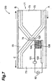
- FIG. 7 is a schematic view showing a second embodiment of the optical switch according to the present invention.
- An optical switch 120 of this embodiment has a movable member 121, and an electrode 122 opposing this movable member 121.
- a comb 124 is formed on the end portion of the movable member 121.
- a comb 125 is formed on that portion of the electrode 122, which opposes the comb 124.
- a mirror 123 for intercepting light propagating on an optical path A is integrated with the end of the movable member 121. In a normal state, this mirror 123 enters a cut portion 74 to intercept light propagating on the optical path A. When the mirror 123 is in this intercepting position, therefore, the mirror surface of this mirror 123 is parallel to the widthwise direction of the optical switch 120. Accordingly, light can be reflected by the mirror 123 without any deterioration of the optical characteristics.
- the third embodiment of the optical switch according to the present invention will be described below with reference to Figs. 8A and 8B.
- the optical switch of this embodiment differs from each embodiment described above in the structure of a position holding mechanism.
- an optical switch 40 of this embodiment has a spring member 41 as a position holding mechanism placed in front of a mirror 9.
- the distal end of this spring member 41 is in contact with the end portion of a movable member 7.
- the proximal end of the spring member 41 is fixed to, e.g., a substrate 72 (see Fig. 2).
- This spring member 41 has spring force which biases the movable member 7.
- this position of the mirror 9 is held by the spring force of the spring member 41.
- FIGs. 9A and 9B show a modification of the optical switch of this embodiment.
- an optical switch 45 has a spring member 46 whose two end portions are fixed to, e.g., a substrate 72 (see Fig. 2), instead of the spring member 41 described above.
- This spring member 46 is coupled with an L-shaped connecting member 47, and the end portion of this connecting member 47 is in contact with the end portion of a movable member 7.
- a movable member 7 is in a state of extending linearly (see Fig. 9A) or in a state of bending (see Fig. 9B)
- this position of the mirror 9 is held by the spring force of the spring member 46.
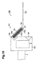
- an optical switch 130 of this embodiment has a position holding mechanism 131.
- This position holding mechanism 131 has a position holding movable portion 133 placed in front of a mirror 9.
- a bent portion 133a which is bent through an angle of, e.g., 45° is formed in the end portion of this position holding movable portion 133.
- This bent portion 133a has a comb 137 having a plurality of teeth 137a.
- a position holding electrode 134 opposes the bent portion 133a.
- This position holding electrode 134 has a comb 138 having a plurality of teeth 138a.
- a holding portion 132 fixing the mirror 9 is formed at the end of a movable member 7.
- This holding portion 132 has a first holding notch 135 for locking the bent portion 133a of the position holding movable portion 133 so as to hold the mirror 9 in an intercepting position, and a second holding notch 136 for locking this bent portion 133a so as to hold the mirror 9 in a through position.
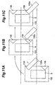
- Figs. 11A to 11C illustrate the procedure of moving the mirror 9 from the first position to the second position in the optical switch 130 as described above.
- First by applying a predetermined voltage across the position holding movable portion 133 and position holding electrode 134, as shown in Fig. 11A, the bent portion 133a locked in the first holding notch 135 is moved toward the position holding electrode 134, thereby unlocking this bent portion 133a.
- the mirror 9 is moved to the second position (see Fig. 11B).
- the position holding mechanism 131 can be driven at a low voltage while its width is decreased to 500 ⁇ m or less.
- optical switch according to the present invention will be described below with reference to Figs. 12 to 16, 17A, and 17B.
- the optical switches of these embodiments are different from the above embodiments in the structure of the movable member or electrode.
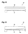
- An optical switch 50 shown in Fig. 12 has a movable member 51 and electrode 52.
- the only difference of the movable member 51 from the movable member 7 and 77 described above is that this movable member 51 has no comb.
- the only difference of the electrode 52 from the electrode 10 and 80 described above is also that this electrode 52 has no comb.
- This electrode 52 extends parallel to the movable member 51 as a whole. In this embodiment, the structures of the movable member 51 and electrode 52 are simplified.
- An optical switch 53 shown in Fig. 13 has a movable member 51 and electrode 54.
- An opposing surface 54a of the electrode 54 which opposes the movable member 51 is curved such that the spacing between this electrode 54 and the movable member 51 decreases from the distal end to the proximal end of the electrode 54.
- the spacing between the movable member 51 and electrode 54 decreases as a whole as the movable member 51 approaches the electrode 54, and this increases the electrostatic force generated between the movable member 51 and electrode 54. Accordingly, as in the previous embodiments, it is possible to lower the driving voltage of the movable member 51 and decrease the length of this movable member 51.
- the opposing surface 54a of the electrode 54 which opposes the movable member 51 is not limited to the curved surface. That is, this opposing surface 54a can also be a linear surface as long as the spacing between the movable member 51 and electrode 54 decreases from the distal end to the proximal end of the electrode 54.
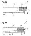
- An optical switch 55 shown in Fig. 14 has a movable member 56 and an electrode 10 described previously.
- a T-shaped comb holder 57 is attached to the end portion of the movable member 56.
- a comb 8 described earlier is formed on this comb holder 57.
- the electrostatic force generated between the movable member 56 and electrode 10 concentrates to the end portion of the movable member 56. This increases the displacement amount of this end portion of the movable member 56. Accordingly, it is possible to further lower the driving voltage of the movable member 56 and further decrease the length of this movable member 56.
- An optical switch 58 shown in Fig. 15 has a movable member 7 described earlier and an electrode 59.
- a notch 60 is formed in that portion of the electrode 59, which opposes a comb 8 of the movable member 7.
- a comb 11 described previously is formed in this notch 60.
- an opposing surface 59a of the electrode 59 which opposes the movable member 7 is a linear surface inclined to the movable member 7, so that the spacing between this movable member 7 and the electrode 59 decreases from the distal end to the proximal end of the electrode 59.
- the surface area of the electrode 59 is increased by the comb 11. Additionally, the spacing between the movable member 7 and electrode 59 decreases as a whole as the movable member 7 approaches the electrode 59, and this increases the electrostatic force generated between the movable member 7 and electrode 59. Accordingly, it is possible to lower the driving voltage of the movable member 7 and decrease the length of this movable member 7.
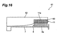
- An optical switch 61 shown in Fig. 16 has a movable member 7 described previously and an electrode 62.
- An opposing surface 62a of the electrode 62 which opposes the movable member 7 is curved such that the spacing between this electrode 62 and the movable member 7 decreases from the distal end to the proximal end of the electrode 62.
- the rest of the arrangement of this electrode 62 is the same as the electrode 59 shown in Fig. 15. Accordingly, the same effects as the optical switch 58 shown in Fig. 15 can be obtained.
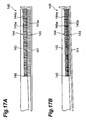
- An optical switch 140 shown in Figs. 17A and 17B has a movable member 141 and electrode 142.
- a comb 143 having a plurality of teeth 143a is formed in the end portion of the movable member 141.
- a notch 145 is formed in that portion of the electrode 142, which opposes the comb 143.
- This notch 145 forms a tapered surface 145a which tapers from the proximal end to the distal end of the electrode 142.
- a comb 144 having a plurality of teeth 144a is formed in this notch 145. These teeth 144a of the comb 144 become longer from the proximal end to the distal end of the electrode 142.
- an optical switch 150 of this embodiment includes a movable member 151 having a mirror 158 at its end.
- a comb 154 having a plurality of teeth 154a is formed on one side of the end portion of this movable member 151.
- a comb 155 having a plurality of teeth 155a is formed on the side away from the comb 154.
- a main electrode 152 is positioned on the side of the comb 154 of this movable member 151. In that portion of this main electrode 152, which opposes the comb 154, a comb 156 having a plurality of teeth 156a to be inserted between the teeth 154a of the comb 154 is formed.
- a returning electrode 153 is positioned on the side of the comb 155 of the movable member 151. In that portion of this returning electrode 153, which opposes the comb 155, a comb 157 having a plurality of teeth 157a to be inserted between the teeth 155a of the comb 155 is formed.
- the movable member 151 and main electrode 152 are connected via a voltage source 159.
- the movable member 151 and returning electrode 153 are connected via a voltage source 160.
- a so-called electrostatic actuator which drives a movable member by generating electrostatic force between this movable member and the electrode is used.
- an electromagnetic actuator or heat actuator can also be used as the means for driving the movable member.
- the optical switch of each of the above embodiments is a 1 ⁇ 2 switch.
- the present invention is also applicable to an optical switch such as an ON/OFF switch or n ⁇ n matrix switch.
- the present invention is suitable applied to the optical switch or optical switch array using in optical communication or the like.
Landscapes
- Physics & Mathematics (AREA)
- General Physics & Mathematics (AREA)
- Optics & Photonics (AREA)
- Engineering & Computer Science (AREA)
- Microelectronics & Electronic Packaging (AREA)
- Mechanical Light Control Or Optical Switches (AREA)
Abstract
Description
Claims (22)
- An optical switch comprising:a base member;a planar waveguide formed on said base member;a movable member cantilevered by said base member wherein a position of its distal end portion in a plane of said planar waveguide is movable by deformation of said movable member;a mirror fixed to the distal end portion of said movable member; anddriving means for switching a light propagation direction in said planar waveguide by deforming said movable member and changing said mirror position with respect to said planar waveguide.
- An optical switch according to claim 1, wherein said driving means comprises a main electrode opposing said movable member, and means for generating electrostatic force between said main electrode and said movable member.
- An optical switch according to claim 2, wherein a spacing between said main electrode and said movable member decreases from the distal end to the proximal end of said electrode.
- An optical switch according to claim 2 or claim 3, wherein
said movable member comprises a first comb having a plurality of teeth, and
a second comb having a plurality of teeth to be inserted between the teeth of said first comb is formed in that portion of said electrode, which opposes said first comb. - An optical switch according to claim 4, wherein a comb supporting portion is formed at the end portion of said movable member, and said first comb is formed on said comb supporting portion.
- An optical switch according to claim 4, wherein the lengths of the teeth of said second comb are made different from each other such that a spacing between the distal end of each tooth of said first comb and the proximal end of each tooth of said second comb increases from the proximal end to the distal end of said main electrode.
- An optical switch according to any one of claims 2 to 6, wherein said driving means further comprises a returning electrode placed on the side of said movable member away from said main electrode, and means for generating electrostatic force between said returning electrode and said movable member.
- An optical switch according to any one of claims 1 to 7, further comprising position holding means for holding said mirror in a first position at which said mirror intercepts light propagating on said optical path and a second position at which said mirror passes light propagating on said optical path.
- An optical switch according to claim 8, wherein said position holding means comprises a position holding movable portion placed in front of said mirror and having a first projection for holding said mirror in the first position and a second projection for holding said mirror in the second position, a position holding driving portion for moving said position holding movable portion in the extending direction of said movable member, and a holding recess which is formed in the end portion of said movable member and into which said first and second projections are inserted.
- An optical switch according to claim 8, wherein said position holding means is a spring member which is placed in front of said mirror, is in contact with the end portion of said movable member, and has spring force which biases said movable member.
- An optical switch according to claim 8, wherein said position holding means comprises a position holding movable portion placed in front of said mirror, a position holding electrode opposing said position holding movable portion, a first holding notch formed in the end portion of said movable member to lock said position holding movable portion such that said mirror is held in the first position, and a second holding notch formed in the end portion of said movable member to lock said position holding movable portion such that said mirror is held in the second position.
- An optical switch according to any one of claims 1 to 11, wherein said movable member is designed such that said mirror intercepts light propagating on said optical path in a normal state.
- An optical switch according to any one of claims 1 to 12, wherein
said planar waveguide comprises a cladding removed portion formed by removing said cladding except for a portion around said core, and a cut portion which is formed on said optical path to connect to said cladding removed portion, and into which said mirror enters, and
said movable member is formed in said cladding removed portion such that said mirror is positioned in the same plane as said core. - An optical switch according to claim 13, wherein said cladding removed portion is formed by removing said cladding by reactive ion etching.
- An optical switch according to claim 13 or 14, wherein said movable member and said mirror are simultaneously formed using the same material.
- An optical switch according to claim 15, wherein said movable member and said mirror are made of silicon.
- An optical switch according to any one of claims 1 to 16, wherein a mirror device comprising said movable member and said mirror is bonded to said planar waveguide.
- An optical switch according to claim 17, an aligning projection is formed on one of said planar waveguide and said mirror device, and an aligning recess which fits on said aligning projection is formed in the other of said planar waveguide and said mirror device.
- An optical switch according to claim 17 or claim 18, wherein said planar waveguide and said mirror device are bonded by anodic bonding.
- An optical switch according to claim 19, wherein a substrate of said planar waveguide is made of silicon or glass containing alkali metal ion.
- An optical switch array disposing a plurality of optical switch according to any one of claims 1 to 20 on same base member.
- An optical array according to claim 21, wherein the array pitch of said mirror devices is not more than 500 µm.
Applications Claiming Priority (3)
| Application Number | Priority Date | Filing Date | Title |
|---|---|---|---|
| JP2001289611A JP2003057569A (en) | 2001-06-07 | 2001-09-21 | Optical switch and optical switch array |
| JP2001289611 | 2001-09-21 | ||
| PCT/JP2002/009642 WO2003027751A1 (en) | 2001-09-21 | 2002-09-19 | Optical switch and optical switch array |
Publications (3)
| Publication Number | Publication Date |
|---|---|
| EP1429170A1 true EP1429170A1 (en) | 2004-06-16 |
| EP1429170A4 EP1429170A4 (en) | 2005-09-07 |
| EP1429170B1 EP1429170B1 (en) | 2008-05-14 |
Family
ID=19112075
Family Applications (1)
| Application Number | Title | Priority Date | Filing Date |
|---|---|---|---|
| EP02767979A Expired - Lifetime EP1429170B1 (en) | 2001-09-21 | 2002-09-19 | Optical switch and optical switch array |
Country Status (6)
| Country | Link |
|---|---|
| US (1) | US6993218B2 (en) |
| EP (1) | EP1429170B1 (en) |
| KR (1) | KR20040044965A (en) |
| CA (1) | CA2461188C (en) |
| DE (1) | DE60226625D1 (en) |
| WO (1) | WO2003027751A1 (en) |
Families Citing this family (7)
| Publication number | Priority date | Publication date | Assignee | Title |
|---|---|---|---|---|
| US7315672B2 (en) * | 2003-11-28 | 2008-01-01 | Sumitomo Electric Industries, Ltd. | Optical device |
| JP2005157163A (en) * | 2003-11-28 | 2005-06-16 | Sumitomo Electric Ind Ltd | Optical device |
| KR100586967B1 (en) * | 2004-05-28 | 2006-06-08 | 삼성전기주식회사 | Rotary comb drive actuator and variable optical attenuator using same |
| JP2007114230A (en) * | 2005-10-17 | 2007-05-10 | Japan Aviation Electronics Industry Ltd | Light switch |
| US9079762B2 (en) * | 2006-09-22 | 2015-07-14 | Ethicon Endo-Surgery, Inc. | Micro-electromechanical device |
| GB2446887A (en) * | 2007-05-04 | 2008-08-27 | Zhou Rong | A 1 |
| MX343770B (en) * | 2014-04-01 | 2016-11-09 | Univ Nac Autónoma De México | Dynamic optical switch. |
Family Cites Families (14)
| Publication number | Priority date | Publication date | Assignee | Title |
|---|---|---|---|---|
| US5226099A (en) * | 1991-04-26 | 1993-07-06 | Texas Instruments Incorporated | Digital micromirror shutter device |
| WO1998009289A1 (en) | 1996-08-27 | 1998-03-05 | Quinta Corporation | Optical head using micro-machined elements |
| US5923798A (en) | 1997-05-15 | 1999-07-13 | Lucent Technologies, Inc. | Micro machined optical switch |
| US5998906A (en) | 1998-01-13 | 1999-12-07 | Seagate Technology, Inc. | Electrostatic microactuator and method for use thereof |
| US6195478B1 (en) * | 1998-02-04 | 2001-02-27 | Agilent Technologies, Inc. | Planar lightwave circuit-based optical switches using micromirrors in trenches |
| US5995688A (en) * | 1998-06-01 | 1999-11-30 | Lucent Technologies, Inc. | Micro-opto-electromechanical devices and method therefor |
| US6108466A (en) * | 1998-09-17 | 2000-08-22 | Lucent Technologies | Micro-machined optical switch with tapered ends |
| JP3219057B2 (en) | 1998-09-24 | 2001-10-15 | 日本電気株式会社 | Variable optical attenuator |
| US6229640B1 (en) | 1999-08-11 | 2001-05-08 | Adc Telecommunications, Inc. | Microelectromechanical optical switch and method of manufacture thereof |
| US6363183B1 (en) * | 2000-01-04 | 2002-03-26 | Seungug Koh | Reconfigurable and scalable intergrated optic waveguide add/drop multiplexing element using micro-opto-electro-mechanical systems and methods of fabricating thereof |
| US6360036B1 (en) * | 2000-01-14 | 2002-03-19 | Corning Incorporated | MEMS optical switch and method of manufacture |
| EP1128201A1 (en) | 2000-02-25 | 2001-08-29 | C.S.E.M. Centre Suisse D'electronique Et De Microtechnique Sa | Switching device, particularly for optical switching |
| JP2002116388A (en) | 2000-10-05 | 2002-04-19 | Sumitomo Electric Ind Ltd | Optical switch and optical switch device including the same |
| US6847753B2 (en) * | 2001-12-14 | 2005-01-25 | Nayef M. Abu-Ageel | Switch-variable optical attenuator and switch arrays |
-
2002
- 2002-09-19 KR KR10-2004-7004088A patent/KR20040044965A/en not_active Withdrawn
- 2002-09-19 US US10/246,761 patent/US6993218B2/en not_active Expired - Fee Related
- 2002-09-19 WO PCT/JP2002/009642 patent/WO2003027751A1/en not_active Ceased
- 2002-09-19 DE DE60226625T patent/DE60226625D1/en not_active Expired - Lifetime
- 2002-09-19 EP EP02767979A patent/EP1429170B1/en not_active Expired - Lifetime
- 2002-09-19 CA CA2461188A patent/CA2461188C/en not_active Expired - Fee Related
Also Published As
| Publication number | Publication date |
|---|---|
| EP1429170B1 (en) | 2008-05-14 |
| DE60226625D1 (en) | 2008-06-26 |
| US6993218B2 (en) | 2006-01-31 |
| EP1429170A4 (en) | 2005-09-07 |
| KR20040044965A (en) | 2004-05-31 |
| WO2003027751A1 (en) | 2003-04-03 |
| CA2461188C (en) | 2011-02-15 |
| US20030103715A1 (en) | 2003-06-05 |
| CA2461188A1 (en) | 2003-04-03 |
Similar Documents
| Publication | Publication Date | Title |
|---|---|---|
| EP1208403B1 (en) | Method of manufacture of a micromechanical optical switch | |
| US6735008B2 (en) | MEMS mirror and method of fabrication | |
| DE60107518T2 (en) | mirror structure | |
| US6839478B2 (en) | Optical switching system based on hollow waveguides | |
| US7504757B2 (en) | Multi-finger z-actuator | |
| WO2001051973A1 (en) | Mems optical switch and method of manufacture | |
| KR100468853B1 (en) | MEMS comb actuator materialized on insulating material and method of manufacturing thereof | |
| US6667823B2 (en) | Monolithic in-plane shutter switch | |
| CA2461188C (en) | Optical switch and optical switch array | |
| US20020164111A1 (en) | MEMS assemblies having moving members and methods of manufacturing the same | |
| US20030012545A1 (en) | Broad-band variable optical attenuator | |
| JP2004102227A (en) | Micro mirror actuator | |
| US6773942B2 (en) | Method for making optical switch array | |
| US6810166B2 (en) | Optical waveguide switch | |
| JP2003057569A (en) | Optical switch and optical switch array | |
| CN100444317C (en) | Micromobile device and manufacturing method thereof | |
| KR100446625B1 (en) | Manufacture method of optical switch | |
| JP2004501382A (en) | Optical switch having moving part and method of manufacturing the same | |
| JP2002116388A (en) | Optical switch and optical switch device including the same | |
| JP2003248182A (en) | Light switch |
Legal Events
| Date | Code | Title | Description |
|---|---|---|---|
| PUAI | Public reference made under article 153(3) epc to a published international application that has entered the european phase |
Free format text: ORIGINAL CODE: 0009012 |
|
| 17P | Request for examination filed |
Effective date: 20040324 |
|
| AK | Designated contracting states |
Kind code of ref document: A1 Designated state(s): AT BE BG CH CY CZ DE DK EE ES FI FR GB GR IE IT LI LU MC NL PT SE SK TR |
|
| A4 | Supplementary search report drawn up and despatched |
Effective date: 20050726 |
|
| RIC1 | Information provided on ipc code assigned before grant |
Ipc: 7G 02B 6/35 B Ipc: 7G 02B 26/08 A |
|
| 17Q | First examination report despatched |
Effective date: 20060215 |
|
| GRAP | Despatch of communication of intention to grant a patent |
Free format text: ORIGINAL CODE: EPIDOSNIGR1 |
|
| GRAS | Grant fee paid |
Free format text: ORIGINAL CODE: EPIDOSNIGR3 |
|
| GRAA | (expected) grant |
Free format text: ORIGINAL CODE: 0009210 |
|
| AK | Designated contracting states |
Kind code of ref document: B1 Designated state(s): DE FR GB IT |
|
| REG | Reference to a national code |
Ref country code: GB Ref legal event code: FG4D |
|
| REF | Corresponds to: |
Ref document number: 60226625 Country of ref document: DE Date of ref document: 20080626 Kind code of ref document: P |
|
| PLBE | No opposition filed within time limit |
Free format text: ORIGINAL CODE: 0009261 |
|
| STAA | Information on the status of an ep patent application or granted ep patent |
Free format text: STATUS: NO OPPOSITION FILED WITHIN TIME LIMIT |
|
| 26N | No opposition filed |
Effective date: 20090217 |
|
| REG | Reference to a national code |
Ref country code: GB Ref legal event code: 746 Effective date: 20121119 |
|
| REG | Reference to a national code |
Ref country code: DE Ref legal event code: R084 Ref document number: 60226625 Country of ref document: DE Effective date: 20121113 |
|
| REG | Reference to a national code |
Ref country code: FR Ref legal event code: PLFP Year of fee payment: 15 |
|
| REG | Reference to a national code |
Ref country code: FR Ref legal event code: PLFP Year of fee payment: 16 |
|
| PGFP | Annual fee paid to national office [announced via postgrant information from national office to epo] |
Ref country code: DE Payment date: 20170912 Year of fee payment: 16 Ref country code: GB Payment date: 20170913 Year of fee payment: 16 |
|
| PGFP | Annual fee paid to national office [announced via postgrant information from national office to epo] |
Ref country code: IT Payment date: 20160921 Year of fee payment: 16 |
|
| REG | Reference to a national code |
Ref country code: FR Ref legal event code: PLFP Year of fee payment: 17 |
|
| PGFP | Annual fee paid to national office [announced via postgrant information from national office to epo] |
Ref country code: FR Payment date: 20180813 Year of fee payment: 17 |
|
| REG | Reference to a national code |
Ref country code: DE Ref legal event code: R119 Ref document number: 60226625 Country of ref document: DE |
|
| GBPC | Gb: european patent ceased through non-payment of renewal fee |
Effective date: 20180919 |
|
| PG25 | Lapsed in a contracting state [announced via postgrant information from national office to epo] |
Ref country code: DE Free format text: LAPSE BECAUSE OF NON-PAYMENT OF DUE FEES Effective date: 20190402 Ref country code: IT Free format text: LAPSE BECAUSE OF NON-PAYMENT OF DUE FEES Effective date: 20180919 |
|
| PG25 | Lapsed in a contracting state [announced via postgrant information from national office to epo] |
Ref country code: GB Free format text: LAPSE BECAUSE OF NON-PAYMENT OF DUE FEES Effective date: 20180919 |
|
| PG25 | Lapsed in a contracting state [announced via postgrant information from national office to epo] |
Ref country code: FR Free format text: LAPSE BECAUSE OF NON-PAYMENT OF DUE FEES Effective date: 20190930 |