EP1428661A2 - Piezoelectric transducers - Google Patents
Piezoelectric transducers Download PDFInfo
- Publication number
- EP1428661A2 EP1428661A2 EP03028768A EP03028768A EP1428661A2 EP 1428661 A2 EP1428661 A2 EP 1428661A2 EP 03028768 A EP03028768 A EP 03028768A EP 03028768 A EP03028768 A EP 03028768A EP 1428661 A2 EP1428661 A2 EP 1428661A2
- Authority
- EP
- European Patent Office
- Prior art keywords
- mesa
- piezoelectric material
- chamber diaphragm
- width
- piezoelectric
- Prior art date
- Legal status (The legal status is an assumption and is not a legal conclusion. Google has not performed a legal analysis and makes no representation as to the accuracy of the status listed.)
- Granted
Links
Images





Classifications
-
- B—PERFORMING OPERATIONS; TRANSPORTING
- B41—PRINTING; LINING MACHINES; TYPEWRITERS; STAMPS
- B41J—TYPEWRITERS; SELECTIVE PRINTING MECHANISMS, i.e. MECHANISMS PRINTING OTHERWISE THAN FROM A FORME; CORRECTION OF TYPOGRAPHICAL ERRORS
- B41J2/00—Typewriters or selective printing mechanisms characterised by the printing or marking process for which they are designed
- B41J2/005—Typewriters or selective printing mechanisms characterised by the printing or marking process for which they are designed characterised by bringing liquid or particles selectively into contact with a printing material
- B41J2/01—Ink jet
- B41J2/135—Nozzles
- B41J2/16—Production of nozzles
- B41J2/1607—Production of print heads with piezoelectric elements
- B41J2/161—Production of print heads with piezoelectric elements of film type, deformed by bending and disposed on a diaphragm
-
- B—PERFORMING OPERATIONS; TRANSPORTING
- B41—PRINTING; LINING MACHINES; TYPEWRITERS; STAMPS
- B41J—TYPEWRITERS; SELECTIVE PRINTING MECHANISMS, i.e. MECHANISMS PRINTING OTHERWISE THAN FROM A FORME; CORRECTION OF TYPOGRAPHICAL ERRORS
- B41J2/00—Typewriters or selective printing mechanisms characterised by the printing or marking process for which they are designed
- B41J2/005—Typewriters or selective printing mechanisms characterised by the printing or marking process for which they are designed characterised by bringing liquid or particles selectively into contact with a printing material
- B41J2/01—Ink jet
- B41J2/135—Nozzles
- B41J2/14—Structure thereof only for on-demand ink jet heads
- B41J2/14201—Structure of print heads with piezoelectric elements
- B41J2/14233—Structure of print heads with piezoelectric elements of film type, deformed by bending and disposed on a diaphragm
-
- B—PERFORMING OPERATIONS; TRANSPORTING
- B41—PRINTING; LINING MACHINES; TYPEWRITERS; STAMPS
- B41J—TYPEWRITERS; SELECTIVE PRINTING MECHANISMS, i.e. MECHANISMS PRINTING OTHERWISE THAN FROM A FORME; CORRECTION OF TYPOGRAPHICAL ERRORS
- B41J2/00—Typewriters or selective printing mechanisms characterised by the printing or marking process for which they are designed
- B41J2/005—Typewriters or selective printing mechanisms characterised by the printing or marking process for which they are designed characterised by bringing liquid or particles selectively into contact with a printing material
- B41J2/01—Ink jet
- B41J2/135—Nozzles
- B41J2/16—Production of nozzles
- B41J2/1621—Manufacturing processes
- B41J2/1623—Manufacturing processes bonding and adhesion
-
- B—PERFORMING OPERATIONS; TRANSPORTING
- B41—PRINTING; LINING MACHINES; TYPEWRITERS; STAMPS
- B41J—TYPEWRITERS; SELECTIVE PRINTING MECHANISMS, i.e. MECHANISMS PRINTING OTHERWISE THAN FROM A FORME; CORRECTION OF TYPOGRAPHICAL ERRORS
- B41J2/00—Typewriters or selective printing mechanisms characterised by the printing or marking process for which they are designed
- B41J2/005—Typewriters or selective printing mechanisms characterised by the printing or marking process for which they are designed characterised by bringing liquid or particles selectively into contact with a printing material
- B41J2/01—Ink jet
- B41J2/135—Nozzles
- B41J2/16—Production of nozzles
- B41J2/1621—Manufacturing processes
- B41J2/1626—Manufacturing processes etching
-
- B—PERFORMING OPERATIONS; TRANSPORTING
- B41—PRINTING; LINING MACHINES; TYPEWRITERS; STAMPS
- B41J—TYPEWRITERS; SELECTIVE PRINTING MECHANISMS, i.e. MECHANISMS PRINTING OTHERWISE THAN FROM A FORME; CORRECTION OF TYPOGRAPHICAL ERRORS
- B41J2/00—Typewriters or selective printing mechanisms characterised by the printing or marking process for which they are designed
- B41J2/005—Typewriters or selective printing mechanisms characterised by the printing or marking process for which they are designed characterised by bringing liquid or particles selectively into contact with a printing material
- B41J2/01—Ink jet
- B41J2/135—Nozzles
- B41J2/16—Production of nozzles
- B41J2/1621—Manufacturing processes
- B41J2/1631—Manufacturing processes photolithography
-
- B—PERFORMING OPERATIONS; TRANSPORTING
- B41—PRINTING; LINING MACHINES; TYPEWRITERS; STAMPS
- B41J—TYPEWRITERS; SELECTIVE PRINTING MECHANISMS, i.e. MECHANISMS PRINTING OTHERWISE THAN FROM A FORME; CORRECTION OF TYPOGRAPHICAL ERRORS
- B41J2/00—Typewriters or selective printing mechanisms characterised by the printing or marking process for which they are designed
- B41J2/005—Typewriters or selective printing mechanisms characterised by the printing or marking process for which they are designed characterised by bringing liquid or particles selectively into contact with a printing material
- B41J2/01—Ink jet
- B41J2/135—Nozzles
- B41J2/16—Production of nozzles
- B41J2/1621—Manufacturing processes
- B41J2/164—Manufacturing processes thin film formation
- B41J2/1642—Manufacturing processes thin film formation thin film formation by CVD [chemical vapor deposition]
-
- B—PERFORMING OPERATIONS; TRANSPORTING
- B41—PRINTING; LINING MACHINES; TYPEWRITERS; STAMPS
- B41J—TYPEWRITERS; SELECTIVE PRINTING MECHANISMS, i.e. MECHANISMS PRINTING OTHERWISE THAN FROM A FORME; CORRECTION OF TYPOGRAPHICAL ERRORS
- B41J2/00—Typewriters or selective printing mechanisms characterised by the printing or marking process for which they are designed
- B41J2/005—Typewriters or selective printing mechanisms characterised by the printing or marking process for which they are designed characterised by bringing liquid or particles selectively into contact with a printing material
- B41J2/01—Ink jet
- B41J2/135—Nozzles
- B41J2/16—Production of nozzles
- B41J2/1621—Manufacturing processes
- B41J2/164—Manufacturing processes thin film formation
- B41J2/1645—Manufacturing processes thin film formation thin film formation by spincoating
-
- B—PERFORMING OPERATIONS; TRANSPORTING
- B41—PRINTING; LINING MACHINES; TYPEWRITERS; STAMPS
- B41J—TYPEWRITERS; SELECTIVE PRINTING MECHANISMS, i.e. MECHANISMS PRINTING OTHERWISE THAN FROM A FORME; CORRECTION OF TYPOGRAPHICAL ERRORS
- B41J2/00—Typewriters or selective printing mechanisms characterised by the printing or marking process for which they are designed
- B41J2/005—Typewriters or selective printing mechanisms characterised by the printing or marking process for which they are designed characterised by bringing liquid or particles selectively into contact with a printing material
- B41J2/01—Ink jet
- B41J2/135—Nozzles
- B41J2/16—Production of nozzles
- B41J2/1621—Manufacturing processes
- B41J2/164—Manufacturing processes thin film formation
- B41J2/1646—Manufacturing processes thin film formation thin film formation by sputtering
-
- H—ELECTRICITY
- H10—SEMICONDUCTOR DEVICES; ELECTRIC SOLID-STATE DEVICES NOT OTHERWISE PROVIDED FOR
- H10N—ELECTRIC SOLID-STATE DEVICES NOT OTHERWISE PROVIDED FOR
- H10N30/00—Piezoelectric or electrostrictive devices
- H10N30/01—Manufacture or treatment
- H10N30/07—Forming of piezoelectric or electrostrictive parts or bodies on an electrical element or another base
- H10N30/072—Forming of piezoelectric or electrostrictive parts or bodies on an electrical element or another base by laminating or bonding of piezoelectric or electrostrictive bodies
- H10N30/073—Forming of piezoelectric or electrostrictive parts or bodies on an electrical element or another base by laminating or bonding of piezoelectric or electrostrictive bodies by fusion of metals or by adhesives
-
- H—ELECTRICITY
- H10—SEMICONDUCTOR DEVICES; ELECTRIC SOLID-STATE DEVICES NOT OTHERWISE PROVIDED FOR
- H10N—ELECTRIC SOLID-STATE DEVICES NOT OTHERWISE PROVIDED FOR
- H10N30/00—Piezoelectric or electrostrictive devices
- H10N30/20—Piezoelectric or electrostrictive devices with electrical input and mechanical output, e.g. functioning as actuators or vibrators
- H10N30/204—Piezoelectric or electrostrictive devices with electrical input and mechanical output, e.g. functioning as actuators or vibrators using bending displacement, e.g. unimorph, bimorph or multimorph cantilever or membrane benders
- H10N30/2047—Membrane type
Definitions
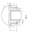
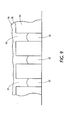
- Figure 11 is a cross-sectional view of the completed bonded product shown in Figures 8 and 9.
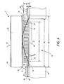
- the minimum mesa thickness Tm chosen, when the piezoelectric material width Wa is greater than the mesa width Wm, should be such that the sum of the thicknesses of the mesa 12, insulative layer 40, and electrical interconnect layer 18 is greater than the sum of the thicknesses of the insulative layer 40, electrical interconnect layer 18, and the dielectric layer 20. This will assure that the piezoelectric material element 22 is in direct contact only on the surface of the mesa 12 and not the top of the dielectric layer 20.
- the mesa thickness Tm for a particular application will be determined by performance and manufacturability constraints. If the mesa thickness Tm is greater than approximately 10% of the chamber diaphragm thickness Tc, there is an added mechanical advantage to the piezoelectric material element 22.
- the criterion in selecting a material for the chamber diaphragm 10 and the chamber support structure 34 are materials suitable for the environment the final structure is to be used in, ease of manufacturability, suitability for subsequent process steps, and appropriate stiffness, commonly described by mechanical elastic modulus and poisson ratio characteristics.
- the stiffness of the chamber diaphragm 10 should be similar to the stiffness characteristics of the piezoelectric material element to be utilized.
- a stiffness ratio of 1/100th to 100 relative to the piezoelectric material element can be used, although it should be noted that there may be some performance degradation as the values diverge.
Landscapes
- Engineering & Computer Science (AREA)
- Manufacturing & Machinery (AREA)
- Measuring Fluid Pressure (AREA)
- Particle Formation And Scattering Control In Inkjet Printers (AREA)
- Reciprocating Pumps (AREA)
- Piezo-Electric Transducers For Audible Bands (AREA)
- Diaphragms For Electromechanical Transducers (AREA)
Abstract
Description
In one embodiment of the piezoelectric transducer of
In a further embodiment the piezoelectric material element width is greater than the mesa width.
In a further embodiment the piezoelectric material element width is greater than the chamber diaphragm width.
In a further embodiment the piezoelectric transducer further comprises a second piezoelectric material element having a second piezoelectric material element width adjacent to the second surface of the chamber diaphragm.
In a further embodiment the piezoelectric transducer further comprises a second mesa having first and second opposing surfaces, a given second mesa thickness, and a given second mesa width interposed between the second piezoelectric material element and the second surface of the chamber diaphragm.
In a further embodiment the second mesa further comprises an insulative layer at least partially on the second surface of the mesa.
In a further embodiment the piezoelectric transducer further comprises an electrical contact layer at least partially interposed between the second piezoelectric material element and the second mesa.
In a further embodiment the second mesa comprises a substantially insulative material.
In a further embodiment the second mesa comprises a substantially conductive material.
In a further embodiment the second chamber diaphragm comprises a substantially conductive material.
In a further embodiment the second chamber diaphragm comprises a substantially non-conductive material.
Further embodiments are described in the appended claims and the following detailed description.
- L
- zero bias line
- N
- neutral surface
- q-
- negative charge
- q+
- positive charge
- Tc
- chamber diaphragm thickness
- Tm
- mesa thickness
- Tm1
- mesa thickness
- Tm2
- mesa thickness
- V
- polarization vector
- Wa
- piezoelectric material width
- Wa1
- piezoelectric material width
- Wa2
- piezoelectric material width
- Wc
- chamber diaphragm width
- Wm
- mesa width
- 1
- piezoelectric transducer
- 10
- chamber diaphragm
- 12
- mesa
- 14
- adhesive
- 16
- chamber
- 18
- electrical interconnect layer
- 20
- dielectric layer
- 22
- piezoelectric material element
- 32
- electrical contact
- 34
- chamber support structure
- 36
- chamber diaphragm lower surface
- 38
- chamber diaphragm upper surface
- 40
- insulative layer
- 42
- electrical contact layer
- 44
- electrical contact layer
- 60
- piezoelectric material element
- 62
- mesa
- 64
- insulative layer
- 66
- electrical interconnect layer
- 68
- adhesive
- 70
- electrical contact layer
- 72
- electrical contact layer
- 74
- electrical contact
For instance, heavily doped silicon, oxides, or nitrides may be used. The chemical etchant can then be used to etch the
Claims (10)
- A piezoelectric transducer comprising:a) a chamber diaphragm having first and second opposing surfaces, a given chamber diaphragm thickness, and a given chamber diaphragm width,b) a mesa having first and second opposing surfaces, a given mesa thickness, and a given mesa width wherein the first surface of the mesa is adjacent to the first surface of the chamber diaphragm, andc) a piezoelectric material element having a given piezoelectric material element width adjacent to the second surface of the mesa.
- The piezoelectric transducer of claim 1 wherein the mesa further comprises an insulative layer at least partially on the second surface of the mesa.
- The piezoelectric transducer of claim 1 further comprising an electrical contact layer at least partially interposed between the piezoelectric material element and the second surface of the mesa.
- The piezoelectric transducer of claim 1 wherein the mesa comprises a substantially insulative material.
- The piezoelectric transducer of claim 1 wherein the mesa comprises a substantially conductive material.
- The piezoelectric transducer of claim 1 wherein the chamber diaphragm comprises a substantially conductive material.
- The piezoelectric transducer of claim 1 wherein the chamber diaphragm comprises a substantially non-conductive material.
- The piezoelectric transducer of claim 1 wherein the mesa thickness is at least approximately 10% of the chamber diaphragm thickness.
- A piezoelectric transducer comprising:a) a chamber diaphragm having first and second opposing surfaces, a given chamber diaphragm thickness, and a given chamber diaphragm width,b) a mesa having first and second opposing surfaces, a given mesa thickness, and a given mesa width wherein the first surface of the mesa is adjacent to the first surface of the chamber diaphragm,c) a piezoelectric material element having a given piezoelectric material element width adjacent to the second surface of the mesa, andd) an electrical interconnect layer interposed between the chamber diaphragm and the mesa.
- A piezoelectric transducer comprising:a) a chamber diaphragm having first and second opposing surfaces, a given chamber diaphragm thickness, and a given chamber diaphragm width,b) mesa having first and second opposing surface, a given mesa thickness, and a given mesa width wherein the first surface of the mesa is adjacent to the first surface of the chamber diaphragm, andc) first and second piezoelectric material elements, each element having a given piezoelectric material element width wherein the first piezoelectric element is adjacent to the second surface of the mesa and the second piezoelectric element is adjacent to second surface of the chamber diaphragm.
Applications Claiming Priority (4)
| Application Number | Priority Date | Filing Date | Title |
|---|---|---|---|
| US43351202P | 2002-12-13 | 2002-12-13 | |
| US433512P | 2002-12-13 | ||
| US664472 | 2003-09-16 | ||
| US10/664,472 US6987348B2 (en) | 2002-12-13 | 2003-09-16 | Piezoelectric transducers |
Publications (3)
| Publication Number | Publication Date |
|---|---|
| EP1428661A2 true EP1428661A2 (en) | 2004-06-16 |
| EP1428661A3 EP1428661A3 (en) | 2004-09-08 |
| EP1428661B1 EP1428661B1 (en) | 2008-11-12 |
Family
ID=32329338
Family Applications (1)
| Application Number | Title | Priority Date | Filing Date |
|---|---|---|---|
| EP03028768A Expired - Lifetime EP1428661B1 (en) | 2002-12-13 | 2003-12-12 | Piezoelectric transducers |
Country Status (3)
| Country | Link |
|---|---|
| EP (1) | EP1428661B1 (en) |
| JP (1) | JP4870904B2 (en) |
| DE (1) | DE60324654D1 (en) |
Cited By (3)
| Publication number | Priority date | Publication date | Assignee | Title |
|---|---|---|---|---|
| JP2012196905A (en) * | 2011-03-22 | 2012-10-18 | Kyocera Corp | Inkjet head, and recording apparatus |
| CN106441665A (en) * | 2016-09-26 | 2017-02-22 | 郑州航空工业管理学院 | Piezoelectric-quartz-wafer's-bending-effect-based bending moment measurement method and sensor |
| CN107396276A (en) * | 2016-05-04 | 2017-11-24 | 英飞凌科技股份有限公司 | Micro-electromechanical device, micro-electromechanical device array, manufacture micro-electromechanical device method and operate micro-electromechanical device method |
Families Citing this family (3)
| Publication number | Priority date | Publication date | Assignee | Title |
|---|---|---|---|---|
| WO2007010909A1 (en) * | 2005-07-19 | 2007-01-25 | Mikuni Corporation | Pressure sensor element and pressure sensor |
| JP5256423B2 (en) * | 2005-07-19 | 2013-08-07 | 株式会社ミクニ | Pressure sensor element and pressure sensor |
| JP5168681B2 (en) * | 2005-12-12 | 2013-03-21 | 独立行政法人産業技術総合研究所 | Tire pressure sensor and tire pressure monitoring device |
Family Cites Families (12)
| Publication number | Priority date | Publication date | Assignee | Title |
|---|---|---|---|---|
| US4613875A (en) * | 1985-04-08 | 1986-09-23 | Tektronix, Inc. | Air assisted ink jet head with projecting internal ink drop-forming orifice outlet |
| JPS63173855A (en) * | 1987-01-12 | 1988-07-18 | Nippon Keiki Seisakusho:Kk | Piezoelectric pump |
| JPH06117377A (en) * | 1992-10-02 | 1994-04-26 | Toshiba Ceramics Co Ltd | Fixed displacement pump |
| JPH07174654A (en) * | 1993-12-20 | 1995-07-14 | Hokuriku Electric Ind Co Ltd | Pressure sensor |
| JPH08205273A (en) * | 1995-01-24 | 1996-08-09 | Mitsubishi Electric Corp | Bone conduction voice vibration detection device and bone conduction voice vibration detection device |
| JPH0976491A (en) * | 1995-09-20 | 1997-03-25 | Nec Corp | Ink jet head |
| JPH09267494A (en) * | 1996-01-31 | 1997-10-14 | Sony Corp | Printer device and method of manufacturing the same |
| US6217158B1 (en) * | 1996-04-11 | 2001-04-17 | Seiko Epson Corporation | Layered type ink jet recording head with improved piezoelectric actuator unit |
| JP3531027B2 (en) * | 1996-10-04 | 2004-05-24 | 株式会社日立製作所 | Micro pumps and pump systems |
| JP3763175B2 (en) * | 1997-02-28 | 2006-04-05 | ソニー株式会社 | Method for manufacturing printer device |
| WO1998052280A1 (en) * | 1997-05-13 | 1998-11-19 | Mitsubishi Denki Kabushiki Kaisha | Piezoelectric thin film device |
| JP2000249074A (en) * | 1999-02-24 | 2000-09-12 | Hitachi Ltd | Micro pump and method of manufacturing the same |
-
2003
- 2003-12-12 DE DE60324654T patent/DE60324654D1/en not_active Expired - Lifetime
- 2003-12-12 EP EP03028768A patent/EP1428661B1/en not_active Expired - Lifetime
- 2003-12-15 JP JP2003417038A patent/JP4870904B2/en not_active Expired - Fee Related
Cited By (4)
| Publication number | Priority date | Publication date | Assignee | Title |
|---|---|---|---|---|
| JP2012196905A (en) * | 2011-03-22 | 2012-10-18 | Kyocera Corp | Inkjet head, and recording apparatus |
| CN107396276A (en) * | 2016-05-04 | 2017-11-24 | 英飞凌科技股份有限公司 | Micro-electromechanical device, micro-electromechanical device array, manufacture micro-electromechanical device method and operate micro-electromechanical device method |
| US10516943B2 (en) | 2016-05-04 | 2019-12-24 | Infineon Technologies Ag | Microelectromechanical device, an array of microelectromechanical devices, a method of manufacturing a microelectromechanical device, and a method of operating a microelectromechanical device |
| CN106441665A (en) * | 2016-09-26 | 2017-02-22 | 郑州航空工业管理学院 | Piezoelectric-quartz-wafer's-bending-effect-based bending moment measurement method and sensor |
Also Published As
| Publication number | Publication date |
|---|---|
| JP4870904B2 (en) | 2012-02-08 |
| EP1428661A3 (en) | 2004-09-08 |
| JP2004198421A (en) | 2004-07-15 |
| EP1428661B1 (en) | 2008-11-12 |
| DE60324654D1 (en) | 2008-12-24 |
Similar Documents
| Publication | Publication Date | Title |
|---|---|---|
| US8237332B2 (en) | Piezoelectric acoustic transducer and method of fabricating the same | |
| CN102006540B (en) | Piezoelectric micro speaker having piston diaphragm and method of manufacturing the same | |
| US5471721A (en) | Method for making monolithic prestressed ceramic devices | |
| JP3521499B2 (en) | Piezoelectric / electrostrictive film type element | |
| US5831371A (en) | Snap-action ferroelectric transducer | |
| US8710716B2 (en) | Actuator, actuator structure and method of manufacturing actuator | |
| US6512323B2 (en) | Piezoelectric actuator device | |
| JP6550387B2 (en) | Multilayer thin film piezoelectric device and method of manufacturing the same | |
| US7992271B2 (en) | Process of manufacturing a piezoelectric actuator for tunable electronic components on a carrier substrate | |
| US5889353A (en) | Piezoelectric/electrostrictive film element with a diaphram having at least one stress releasing end section | |
| US8847466B2 (en) | Piezoelectric bimorph switch | |
| US6987348B2 (en) | Piezoelectric transducers | |
| JP7091699B2 (en) | Manufacturing method of ultrasonic sensor, ultrasonic device, and ultrasonic sensor | |
| CN107396276B (en) | Microelectromechanical device, array of microelectromechanical devices, method of making a microelectromechanical device, and method of operating a microelectromechanical device | |
| US6924584B2 (en) | Piezoelectric transducers utilizing sub-diaphragms | |
| US6967431B2 (en) | Piezoelectric transducers and methods of manufacture | |
| EP1428661B1 (en) | Piezoelectric transducers | |
| US8450912B2 (en) | Actuator element, method of driving actuator element, method of manufacturing actuator element, device inspection method and MEMS switch | |
| US20040115396A1 (en) | Product and process for bonding porous materials to substrates | |
| WO1994002965A1 (en) | Ceramic deflection device | |
| US20040112530A1 (en) | Product and process for bonding porous materials to substrates | |
| Haertling | Method for making monolithic prestressed ceramic devices |
Legal Events
| Date | Code | Title | Description |
|---|---|---|---|
| PUAI | Public reference made under article 153(3) epc to a published international application that has entered the european phase |
Free format text: ORIGINAL CODE: 0009012 |
|
| AK | Designated contracting states |
Kind code of ref document: A2 Designated state(s): AT BE BG CH CY CZ DE DK EE ES FI FR GB GR HU IE IT LI LU MC NL PT RO SE SI SK TR |
|
| AX | Request for extension of the european patent |
Extension state: AL LT LV MK |
|
| PUAL | Search report despatched |
Free format text: ORIGINAL CODE: 0009013 |
|
| AK | Designated contracting states |
Kind code of ref document: A3 Designated state(s): AT BE BG CH CY CZ DE DK EE ES FI FR GB GR HU IE IT LI LU MC NL PT RO SE SI SK TR |
|
| AX | Request for extension of the european patent |
Extension state: AL LT LV MK |
|
| 17P | Request for examination filed |
Effective date: 20050308 |
|
| AKX | Designation fees paid |
Designated state(s): DE FR GB |
|
| 17Q | First examination report despatched |
Effective date: 20070316 |
|
| GRAP | Despatch of communication of intention to grant a patent |
Free format text: ORIGINAL CODE: EPIDOSNIGR1 |
|
| GRAS | Grant fee paid |
Free format text: ORIGINAL CODE: EPIDOSNIGR3 |
|
| GRAA | (expected) grant |
Free format text: ORIGINAL CODE: 0009210 |
|
| AK | Designated contracting states |
Kind code of ref document: B1 Designated state(s): DE FR GB |
|
| REG | Reference to a national code |
Ref country code: GB Ref legal event code: FG4D |
|
| REF | Corresponds to: |
Ref document number: 60324654 Country of ref document: DE Date of ref document: 20081224 Kind code of ref document: P |
|
| PLBE | No opposition filed within time limit |
Free format text: ORIGINAL CODE: 0009261 |
|
| STAA | Information on the status of an ep patent application or granted ep patent |
Free format text: STATUS: NO OPPOSITION FILED WITHIN TIME LIMIT |
|
| 26N | No opposition filed |
Effective date: 20090813 |
|
| REG | Reference to a national code |
Ref country code: FR Ref legal event code: PLFP Year of fee payment: 13 |
|
| REG | Reference to a national code |
Ref country code: FR Ref legal event code: PLFP Year of fee payment: 14 |
|
| PGFP | Annual fee paid to national office [announced via postgrant information from national office to epo] |
Ref country code: FR Payment date: 20161121 Year of fee payment: 14 Ref country code: GB Payment date: 20161128 Year of fee payment: 14 Ref country code: DE Payment date: 20161121 Year of fee payment: 14 |
|
| REG | Reference to a national code |
Ref country code: DE Ref legal event code: R119 Ref document number: 60324654 Country of ref document: DE |
|
| GBPC | Gb: european patent ceased through non-payment of renewal fee |
Effective date: 20171212 |
|
| REG | Reference to a national code |
Ref country code: FR Ref legal event code: ST Effective date: 20180831 |
|
| PG25 | Lapsed in a contracting state [announced via postgrant information from national office to epo] |
Ref country code: FR Free format text: LAPSE BECAUSE OF NON-PAYMENT OF DUE FEES Effective date: 20180102 Ref country code: DE Free format text: LAPSE BECAUSE OF NON-PAYMENT OF DUE FEES Effective date: 20180703 |
|
| PG25 | Lapsed in a contracting state [announced via postgrant information from national office to epo] |
Ref country code: GB Free format text: LAPSE BECAUSE OF NON-PAYMENT OF DUE FEES Effective date: 20171212 |