EP1426942A2 - Storage device - Google Patents
Storage device Download PDFInfo
- Publication number
- EP1426942A2 EP1426942A2 EP03013960A EP03013960A EP1426942A2 EP 1426942 A2 EP1426942 A2 EP 1426942A2 EP 03013960 A EP03013960 A EP 03013960A EP 03013960 A EP03013960 A EP 03013960A EP 1426942 A2 EP1426942 A2 EP 1426942A2
- Authority
- EP
- European Patent Office
- Prior art keywords
- substrate
- layer
- rotor
- storage device
- phase change
- Prior art date
- Legal status (The legal status is an assumption and is not a legal conclusion. Google has not performed a legal analysis and makes no representation as to the accuracy of the status listed.)
- Withdrawn
Links
Images




Classifications
-
- G—PHYSICS
- G11—INFORMATION STORAGE
- G11B—INFORMATION STORAGE BASED ON RELATIVE MOVEMENT BETWEEN RECORD CARRIER AND TRANSDUCER
- G11B9/00—Recording or reproducing using a method not covered by one of the main groups G11B3/00 - G11B7/00; Record carriers therefor
- G11B9/10—Recording or reproducing using a method not covered by one of the main groups G11B3/00 - G11B7/00; Record carriers therefor using electron beam; Record carriers therefor
-
- B—PERFORMING OPERATIONS; TRANSPORTING
- B82—NANOTECHNOLOGY
- B82Y—SPECIFIC USES OR APPLICATIONS OF NANOSTRUCTURES; MEASUREMENT OR ANALYSIS OF NANOSTRUCTURES; MANUFACTURE OR TREATMENT OF NANOSTRUCTURES
- B82Y10/00—Nanotechnology for information processing, storage or transmission, e.g. quantum computing or single electron logic
-
- G—PHYSICS
- G11—INFORMATION STORAGE
- G11B—INFORMATION STORAGE BASED ON RELATIVE MOVEMENT BETWEEN RECORD CARRIER AND TRANSDUCER
- G11B11/00—Recording on or reproducing from the same record carrier wherein for these two operations the methods are covered by different main groups of groups G11B3/00 - G11B7/00 or by different subgroups of group G11B9/00; Record carriers therefor
- G11B11/08—Recording on or reproducing from the same record carrier wherein for these two operations the methods are covered by different main groups of groups G11B3/00 - G11B7/00 or by different subgroups of group G11B9/00; Record carriers therefor using recording by electric charge or by variation of electric resistance or capacitance
-
- G—PHYSICS
- G11—INFORMATION STORAGE
- G11B—INFORMATION STORAGE BASED ON RELATIVE MOVEMENT BETWEEN RECORD CARRIER AND TRANSDUCER
- G11B9/00—Recording or reproducing using a method not covered by one of the main groups G11B3/00 - G11B7/00; Record carriers therefor
- G11B9/12—Recording or reproducing using a method not covered by one of the main groups G11B3/00 - G11B7/00; Record carriers therefor using near-field interactions; Record carriers therefor
- G11B9/14—Recording or reproducing using a method not covered by one of the main groups G11B3/00 - G11B7/00; Record carriers therefor using near-field interactions; Record carriers therefor using microscopic probe means, i.e. recording or reproducing by means directly associated with the tip of a microscopic electrical probe as used in Scanning Tunneling Microscopy [STM] or Atomic Force Microscopy [AFM] for inducing physical or electrical perturbations in a recording medium; Record carriers or media specially adapted for such transducing of information
Definitions
- U.S. Patent No. 5,557,596 discloses an ultra-high-density storage device.
- This ultra-high density storage device includes at least one field emitter in close proximity to a storage medium, and a micromover for moving the storage medium relative to the field emitter.
- Each field emitter can generate an electron beam current.
- the storage medium may have more than one storage area on it, and a field emitter may be assigned to each storage area, or to multiple storage areas.
- the power density of an electron beam current generated by the field emitter is adjusted to change the state of the storage area bombarded by the electron beam current. Above certain current thresholds, different physical state changes can be made in the storage area being bombarded by the electron beam current. If two physical states are used, then each location in a storage area would have a binary data potential. Since more than two physical states are possible in a given location, more than binary data levels are possible in each location.
- the power density of the electron beam current may be reduced to generate a signal current from the storage area bombarded by the electron beam current. During reading, the power density is selected to be low enough so that no writing occurs.
- the magnitude of the signal current depends on the physical state of the storage area.
- the information stored in the storage area is read by measuring the magnitudes of the signal current.
- the micromover is able to position the storage medium with respect to the field emitters so that each field emitter can access many storage locations within one or more storage areas.
- Each of the storage areas, or data clusters may have an area of phase change material which is coupled to a highly conductive silicon substrate. While the data clusters of phase change material are isolated from each other, their common silicon substrate does not allow for differential signal processing of the individual media patches.
- FIG. 1 schematically illustrates an embodiment of a storage device in a side cross-sectional view.
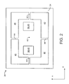
- FIG. 2 is a cross-sectional top view of the embodied storage device of FIG. 1.
- FIG. 3 schematically illustrates one embodiment of data reading circuitry for the storage device of FIG. 1.
- FIGS. 4A-4F schematically illustrate, in side cross-sectional views, one embodiment of a method to isolate data clusters for a storage device.
- FIG. 5 is a top view of the isolated data clusters schematically illustrated in FIG. 4F.
- FIG. 6 schematically illustrates an embodiment of a storage device, utilizing the isolated data clusters of FIG. 4F, in a side cross-sectional view.
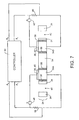
- FIG. 7 schematically illustrates one embodiment of data reading circuitry for the storage device of FIG. 6.
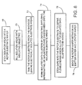
- FIG. 8 is a flowchart illustrating one embodiment of actions which may be used to isolate data clusters for a storage device.
- FIG. 9 schematically illustrates one embodiment of isolated data clusters for a storage device in a side cross-sectional view.
- FIG. 10 is a top view of the isolated data clusters schematically illustrated in FIG. 9.
- FIG. 1 schematically illustrates an embodiment of a storage device 20 in a side cross-sectional view.
- the storage device 20 has three layers which are bonded together, including an emitter layer 22, a rotor layer 24, and a stator layer 26.
- Bonding surfaces 28 may be constructed as part of either of the layers 22, 24, 26 prior to bonding, or may be separate elements.
- the bonding surfaces 28 may also be conductive or contain conductive traces in order to allow electrical coupling between the layers 22, 24, 26.
- the emitter layer 22 has one or more field emitters 30, and a gate 32 for each field emitter 30.
- the field emitters 30 have a sharp point with a radius of curvature sized such that when a preselected potential difference is applied between a field emitter 30 and its corresponding gate 32, an electron beam current is released from the point of the field emitter 30 towards the rotor layer 24.
- the field emitters 30 are illustrated as having a point, field emitters with other shapes may be desirable, such as flat field emitters, depending on a given application.
- the rotor layer 24 has a substrate 34, typically made of a crystalline structure, such as silicon which has been doped to be highly conductive. Patches of phase change media 36 are coupled to the substrate 34.
- the stator layer 26 and the rotor layer 24 interact with each other through an actuation mechanism, here schematically illustrated as actuator 38.
- actuator 38 is schematically illustrated as physically coupled between the stator layer 26 and the rotor layer 24, no physical connection is necessary. While piezoelectric actuators, and the like, may be physically coupled between the stator layer 26 and the rotor layer 24, non-contact methods for actuation may be used.
- electrodes may be formed on the stator layer 26 and on the rotor layer 24, facing each other, and may be aligned such that varying voltages to certain electrodes serve to move the rotor layer 24 as the electrodes position themselves within the resultant electric fields.
- FIG. I illustrates the actuator 38 schematically for ease of understanding, but it should be understood that all contact and non-contact methods of moving the rotor layer 24 may be compatible with storage devices.
- the rotor layer 24 defines a series of gaps 40 which allow a portion of the rotor layer 24 to be moved by the actuator 38.
- the gaps 40 may be better seen in FIG. 2.
- FIG. 2 is a cross-sectional top view of the embodied storage device 20 of FIG. 1, taken along section line 2-2, and showing the rotor layer 24.
- the moveable portion of the rotor layer 24 is often referred to as a micromover 42.
- the micromover 42 is defined by the gaps 40 and beams 44. Beams 44 are manufactured thin enough to allow them to flex, thereby allowing movement of the micromover 42 back and forth along the X-axis and the Y-axis, or combinations thereof, when actuated by the actuator 38.
- the micromover 42 has patches of phase change media 36 in different locations.
- each field emitter 30 is positioned over a corresponding patch of phase change media 36.
- one field emitter 30 may be allocated for several patches of phase change media 36.
- Each patch of phase change media 36 may also be referred to as a data cluster 45.
- the field emitter 30 is positioned in a particular location over a data cluster 45, the emitter 30 is said to be over a storage location.
- an electron beam current is released from the field emitter 30 towards the rotor layer 24, it will contact a storage location in a data cluster 45.
- the storage density of each data cluster 45 may be determined by the number of unique storage locations which the micromover 42 may be moved to. The number of unique storage locations are determined in great part by the spot size of the electron beam.
- FIG. 3 schematically illustrates one embodiment of data-reading circuitry for the storage device of FIG. 1.
- the only layer of the storage device 20 which is shown is the rotor layer 24. This is done for ease of explanation, however, it should be understood that the storage device 20 has three layers 22, 24, 26 which are bonded together as discussed with respect to FIG. 1.
- Fig. 3 shows the positive end of bias voltage 46 coupled to a first data cluster 45.
- the negative end of bias voltage 46 is coupled to a common ground 50 through a first current limiting resistor 52.
- the positive end of bias voltage 48 is coupled to a second data cluster 45.
- the negative end of bias voltage 48 is coupled to the common ground 50 through a second current limiting resistor 52.
- a controller 54 may be provided to monitor the states of the data clusters 45 during data reading periods.
- One of the data clusters 45 is coupled to controller 54 at input A.
- the other data cluster 45 is coupled to the controller 54 at input B.
- Electron beam currents may be emitted from field emitters 30 and aimed at data clusters 45. Electron beam currents below a threshold (determined by the phase change media 36) will not change the physical properties of the media 36. In this case, excitation from the electron beam at a storage location will cause current to flow from the data cluster 45, through the substrate 34. When there is no electron beam excitation, there is no current flowing through the data clusters 45 and the substrate 34, so the inputs A and B will see the voltage provided by the bias voltages 46 and 48, respectively.
- the voltage sensed at inputs A and B will depend on the physical state of the phase change media 36 to which they are coupled. For example, if the phase change media coupled to input A is in a first physical state at a particular data location, then electron beam excitation at that data location might cause the controller 54 to see a lower voltage at input A (compared to the bias voltage 46) during excitation because current flows easily through the phase change media 36 and the substrate 34 to ground 50.
- Controller 54 may be a suitably programmed microprocessor, an Application Specific Integrated Circuit (ASIC), discreet analog components, digital components, or any combination or equivalent thereof. Signals read by the controller 54 are common mode signals.
- ASIC Application Specific Integrated Circuit
- FIGS. 4A-4F schematically illustrate, in side cross-sectional views, one embodiment of a method to isolate data clusters for a storage device.
- FIG. 4A shows a starting slab of material which is intended to form the substrate 34 in the rotor layer 24.
- Substrate 34 is typically chosen to be crystalline silicon which has been doped to be highly conductive.
- deep trenches 56 are etched into the substrate 34 as shown in FIG. 4B.
- the trenches 56 are etched such that they will be positioned around the locations where the data clusters 45 will be formed.
- the trenches 56 are then filled with an insulating dielectric material 58 as shown in FIG. 4C.
- FIG. 4C In the embodiment of FIG.
- the single dielectric material 58 completely fills the trenches 56.
- Suitable dielectric materials may be nitrides and oxides, such as aluminum-oxide, silicon-dioxide, and silicon-nitride, as well as high resistivity polycrystalline silicon.
- the substrate 34 is then thinned from the backside 59 up to a level illustrated as dashed line 60. Backside thinning may be accomplished by a variety of chemical or mechanical abrasion processes. After backside thinning, the rotor layer 24 has taken on the form illustrated in FIG. 4D, where the dielectric material 58 can electrically isolate areas of the substrate 34, such as substrate areas 34A and 34B.
- the dielectric material 58 is also mechanically supporting the substrate areas 34A, 34B, and may even be selected to provide tensile and compression characteristics of the rotor layer 24 which will either make the micromover 42 more or less flexible, as desired.
- the phase change media 36 is deposited in the substrate areas 34A and 34B, between the dielectric material 58. Although the phase change media 36 is shown as being deposited or layered on top of the substrate areas 34A, 34B, the phase change media 36 may also be impregnated or diffused into the surface of the substrate areas 34A and 34B.
- the substrate 34 is etched to define gaps 40, leaving beams 44 to support the micromover 42 of the rotor layer 24.
- FIG. 5 is a top view of the rotor layer 24 schematically illustrated in FIG. 4F.
- the gaps 40 and the beams 44 can be more clearly appreciated.
- the dielectric material 58 which surrounds and isolates the data clusters 45 is also shown.
- FIGS. 4A-4F isolation is established without needing to rely on relatively high temperature processes to remove portions of the substrate 34 after bonding of the emitter, rotor, and stator layers 22, 24, 26.
- the formation of the rotor layer 24 in FIGS. 4A-4F is not likely to introduce additional steps in the fabrication process flow, since deep trench etching and oxide backfill may already be used in formation of the through-wafer connections (not shown). Formation of the connections on the storage device and masking steps, such as lithographic techniques, which are employed in the fabrication of semiconductor devices are not discussed, as such techniques are varied, compatible with this disclosure, and known to those skilled in the art.
- FIG. 6 schematically illustrates an embodiment of a storage device 62 in a side cross-sectional view.
- the storage device 62 has three layers which are bonded together, including an emitter layer 22, a rotor layer 24, and a stator layer 26.
- the rotor layer 24 illustrated in FIG. 6 is the rotor layer 24 previously discussed in FIGS. 4F and 5.
- Bonding surfaces 28 may be constructed as part of either of the layers 22, 24, 26 prior to bonding, or may be separate elements.
- the bonding surfaces 28 may also be conductive or contain conductive traces in order to allow electrical coupling between the layers 22, 24, 26.
- the emitter layer has one or more field emitters 30, and a gate 32 for each field emitter 30.
- actuator 38 The stator layer 26 and the rotor layer 24 interact with each other through an actuation mechanism, here schematically illustrated as actuator 38.
- actuator 38 is schematically illustrated as physically coupled between the stator layer 26 and the rotor layer 24, no physical connection is necessary.
- piezoelectric actuators, and the like may be physically coupled between the stator layer 26 and the rotor layer 24, both non-contact and contact methods of activating or moving the micromover 42 of the rotor layer 24 may be used, as previously discussed.
- FIG. 7 schematically illustrates one embodiment of data-reading circuitry for the storage device of FIG. 6.
- FIG. 7 shows the positive end of bias voltage 46 coupled to the data cluster 45 associated with substrate 34A.
- the positive end of bias voltage 48 is coupled to the data cluster 45 associated with substrate 34B.
- the negative end of bias voltage 46 is coupled to a first side of resistor 64.
- the negative end of bias voltage 48 is coupled to a first side of resistor 66.
- the substrate 34A is coupled to a second side of resistor 64, and the substrate 34B is coupled to a second side of resistor 66.
- a controller 54 is provided to monitor the states of the data clusters 45 during data reading periods.
- the first side of resistor 64 is coupled to controller 54 at input A 1 .
- the second side of resistor 64 is coupled to controller 54 at input A 2 .
- the difference in voltage potential across resistor 64 will be sensed by the controller 54, and this difference may be correlated to the data state of storage locations within the data cluster 45 associated with substrate 34A.
- the first side of resistor 66 is coupled to controller 54 at input B 1 .
- the second side of resistor 66 is coupled to controller 54 at input B 2 .
- the difference in voltage potential across resistor 66 will be sensed by the controller 54, and this difference may be correlated to the data state of storage locations within the data cluster 45 associated with substrate 34B.
- Electron beam currents may be emitted from field emitters 30 and aimed at data clusters 45. Electron beam currents below a threshold (determined by the phase change media 36) will not change the physical properties of the media 36. In this case, excitation from the electron beam at a storage location will cause current to flow from the data clusters 45, through the substrate 34A or the substrate 34B, depending on which data cluster or clusters are being used. In the case of the data cluster 45 associated with substrate 34A, when there is no electron beam excitation, there is no current flowing through the data cluster 45 and the substrate 34A, therefore there is no current flowing through the resistor 64. Thus, the inputs A 1 and A 2 will see no potential difference across resistor 64.
- phase change media 36 is in a second physical state (more conductive than the first state) at a particular data location
- the same electron beam excitation at that data location might cause the controller 54 to see a higher potential difference between inputs A 1 and A 2 (compared to the potential difference when the media is in the first physical state).
- the controller 54 can then associate the varying potential differences between inputs A 1 and A 2 with binary or multi-level data values for data locations within the data cluster 45.
- the data cluster 45 associated with substrate 34B and inputs B 1 and B 2 would operate in a similar fashion.
- This embodiment utilizes electrically isolated media patches 36, enabling differential signal detection, thereby resulting in much lower electrical noise.
- Functionally and structurally equivalent circuitry may be substituted for the circuitry schematically illustrated in FIG.
- Controller 54 may be a suitably programmed microprocessor, an Application Specific Integrated Circuit (ASIC), discreet analog components, digital components, or any combination or equivalent thereof.
- ASIC Application Specific Integrated Circuit
- Signals read by the controller 54 in FIG. 7 are differential mode signals.
- FIG. 8 is a flowchart illustrating one embodiment of actions which may be used to isolate data clusters for a storage device 62.
- Isolation areas are etched 68 into a rotor substrate wafer.
- the isolation areas are filled 70 with an insulating dielectric.
- the rotor substrate is thinned 72 from the backside, leaving electrically isolated substrate areas.
- Isolated data clusters are formed 74 by depositing, diffusing, impregnating, or implanting a phase change media onto the electrically isolated substrate areas.
- Gaps are etched 76 into the rotor substrate to define flexible beams which allow the isolated data clusters to be moved.
- the rotor wafer (or rotor layer) is bonded 78 between an emitter wafer (or emitter layer) and a stator wafer (or stator layer).
- FIG. 8 schematically illustrates one embodiment of isolated data clusters for a storage device in a cross-sectional side view.
- FIG. 10 is a top view of the isolated data clusters schematically illustrated in FIG. 9.
- the dielectric material 58 has been placed throughout the micromover 42, not just around data clusters 45.
- the isolation areas may be etched and filled with insulating dielectric to adjust the modulus of the micromover through the ratio and layout of the insulating dielectric with respect to the substrate.
- the embodied storage devices 20, 62 were illustrated as having one electron field emitter 30 for each data cluster 45, it should be understood that a single field emitter 30 can be used to access more than one data cluster, depending on a particular storage device design, and these types of storage devices and their equivalents are deemed to be within the scope of the claims below.
- Micromover isolation techniques were discussed with respect to storage devices, however, the disclosed isolation techniques may also be applicable to other micromover devices where isolation is required on highly conductive substrates. Additionally, it is apparent that a variety of other structurally and functionally equivalent modifications and substitutions may be made to implement data cluster isolation or isolation on a micromover device according to the concepts covered herein, depending upon the particular implementation, while still falling within the scope of the claims below.
Landscapes
- Engineering & Computer Science (AREA)
- Physics & Mathematics (AREA)
- Chemical & Material Sciences (AREA)
- Nanotechnology (AREA)
- Plasma & Fusion (AREA)
- Mathematical Physics (AREA)
- Theoretical Computer Science (AREA)
- Crystallography & Structural Chemistry (AREA)
- Semiconductor Memories (AREA)
- Induction Machinery (AREA)
- Windings For Motors And Generators (AREA)
Abstract
Description
Claims (10)
- A storage device (62), comprising
a stator layer (26);
an emitter layer (22); and
a rotor layer (24), wherein the rotor layer (24) comprises a plurality of data clusters (45), each having a substrate (34A, 34B) which is electrically isolated from the other data clusters (45) by a dielectric material (58). - The storage device (62) of claim 1, wherein the rotor layer (24) is bonded between the emitter layer (22) and the stator layer (26).
- The storage device (62) of claim 2, wherein the stator layer (26) and the rotor layer (24) are coupled together by an actuator (38).
- The storage device (62) of claim 1, wherein the data clusters (45) comprise a phase change media (36).
- The storage device (62) of claim 1, further comprising:first conductive bonding surfaces (28) which couple the emitter layer (22) to the rotor layer (24); andsecond conductive bonding surfaces (28) which couple the rotor layer (24) to the stator layer (26).
- A storage device (62), comprising:means for electrically isolating a plurality of data clusters (45), of phase change media (36) coupled to a conductive substrate (34A, 34B), from each other; andmeans for reading a differential signal (FIG. 7) from each of the data clusters (45) based on currents which flow from the phase change media (36) to the conductive substrate (34A, 34B) in each data cluster (45).
- A method of reading data from a storage device (62), comprising:generating an electron beam current incident on a storage location (45) comprising a phase change media (36) and a substrate (34A, 34B); anddifferentially measuring (FIG. 7) an electrical signal between the phase change media and the substrate.
- A method of electrically isolating conductive regions on a micromover device, comprising:etching (68) isolation areas (56) into a rotor substrate wafer (24);filling (70) the isolation areas (56) with an insulating dielectric (58);thinning (72) the rotor substrate wafer (24) from the backside (59), leaving electrically isolated substrate areas (34A, 34B);etching (76) gaps (40) into the rotor substrate wafer (24) to define flexible beams (44) which allow the isolated substrate areas (34A, 34B) to be moved; andbonding (78) the rotor wafer (24) between a second wafer (22) and a stator wafer (26).
- The method of claim 8, wherein the micromover device is a storage device (62) and the second wafer is an emitter wafer (22), the method further comprising:after thinning (72) the rotor substrate, depositing, diffusing, impregnating, or implanting (74) a phase change media (36) onto the isolated substrate areas (34A, 34B).
- The method of claim 14, wherein the isolation areas are etched and filled with insulating dielectric to adjust the modulus of the micromover through the ratio and layout of the insulating dielectric with respect to the substrate (FIGS. 9, 10).
Applications Claiming Priority (2)
| Application Number | Priority Date | Filing Date | Title |
|---|---|---|---|
| US310606 | 2002-12-05 | ||
| US10/310,606 US6961299B2 (en) | 2002-12-05 | 2002-12-05 | Storage device |
Publications (2)
| Publication Number | Publication Date |
|---|---|
| EP1426942A2 true EP1426942A2 (en) | 2004-06-09 |
| EP1426942A3 EP1426942A3 (en) | 2006-01-25 |
Family
ID=32312278
Family Applications (1)
| Application Number | Title | Priority Date | Filing Date |
|---|---|---|---|
| EP03013960A Withdrawn EP1426942A3 (en) | 2002-12-05 | 2003-06-20 | Storage device |
Country Status (4)
| Country | Link |
|---|---|
| US (1) | US6961299B2 (en) |
| EP (1) | EP1426942A3 (en) |
| JP (1) | JP2004185801A (en) |
| TW (1) | TW200410396A (en) |
Cited By (4)
| Publication number | Priority date | Publication date | Assignee | Title |
|---|---|---|---|---|
| WO2007138035A1 (en) * | 2006-05-30 | 2007-12-06 | Commissariat A L'energie Atomique | Memory data writable and readable by micropoints, box structures and the manufacturing method |
| WO2009086084A1 (en) * | 2007-12-19 | 2009-07-09 | Contour Semiconductor, Inc. | Field-emitter-based memory array with phase-change storage devices |
| US8455298B2 (en) | 2008-08-18 | 2013-06-04 | Contour Semiconductor, Inc. | Method for forming self-aligned phase-change semiconductor diode memory |
| US8773881B2 (en) | 2009-03-10 | 2014-07-08 | Contour Semiconductor, Inc. | Vertical switch three-dimensional memory array |
Families Citing this family (2)
| Publication number | Priority date | Publication date | Assignee | Title |
|---|---|---|---|---|
| US20040218508A1 (en) * | 2003-04-30 | 2004-11-04 | Zhizhang Chen | Data cluster erasure |
| US7380050B2 (en) * | 2005-01-31 | 2008-05-27 | Van Lydegraf Curt N | Parallel data storage device |
Family Cites Families (9)
| Publication number | Priority date | Publication date | Assignee | Title |
|---|---|---|---|---|
| JPH05282717A (en) * | 1992-03-31 | 1993-10-29 | Canon Inc | Recording medium manufacturing method, recording medium, and information processing apparatus |
| US5557596A (en) * | 1995-03-20 | 1996-09-17 | Gibson; Gary | Ultra-high density storage device |
| US6121552A (en) * | 1997-06-13 | 2000-09-19 | The Regents Of The University Of Caliofornia | Microfabricated high aspect ratio device with an electrical isolation trench |
| JP3978818B2 (en) * | 1997-08-08 | 2007-09-19 | ソニー株式会社 | Manufacturing method of micro head element |
| JP3519623B2 (en) * | 1998-03-13 | 2004-04-19 | 株式会社東芝 | Recording medium and method for manufacturing the same |
| US6574257B1 (en) * | 2000-02-01 | 2003-06-03 | Siros Technologies, Inc. | Near-field laser and detector apparatus and method |
| US6542400B2 (en) * | 2001-03-27 | 2003-04-01 | Hewlett-Packard Development Company Lp | Molecular memory systems and methods |
| US6643248B2 (en) * | 2001-04-16 | 2003-11-04 | Hewlett-Packard Development Company, L.P. | Data storage device |
| US6700853B2 (en) * | 2001-07-20 | 2004-03-02 | Hewlett-Packard Development Company, Lp. | Data storage devices with wafer alignment compensation |
-
2002
- 2002-12-05 US US10/310,606 patent/US6961299B2/en not_active Expired - Lifetime
-
2003
- 2003-06-17 TW TW092116408A patent/TW200410396A/en unknown
- 2003-06-20 EP EP03013960A patent/EP1426942A3/en not_active Withdrawn
- 2003-12-01 JP JP2003401282A patent/JP2004185801A/en not_active Withdrawn
Cited By (7)
| Publication number | Priority date | Publication date | Assignee | Title |
|---|---|---|---|---|
| WO2007138035A1 (en) * | 2006-05-30 | 2007-12-06 | Commissariat A L'energie Atomique | Memory data writable and readable by micropoints, box structures and the manufacturing method |
| FR2901909A1 (en) * | 2006-05-30 | 2007-12-07 | Commissariat Energie Atomique | INSCRIPTIBLE AND MICROPOINT-READABLE DATA MEMORY, BUILT STRUCTURE, AND METHOD OF MANUFACTURE |
| WO2009086084A1 (en) * | 2007-12-19 | 2009-07-09 | Contour Semiconductor, Inc. | Field-emitter-based memory array with phase-change storage devices |
| US8000129B2 (en) | 2007-12-19 | 2011-08-16 | Contour Semiconductor, Inc. | Field-emitter-based memory array with phase-change storage devices |
| US8455298B2 (en) | 2008-08-18 | 2013-06-04 | Contour Semiconductor, Inc. | Method for forming self-aligned phase-change semiconductor diode memory |
| US8773881B2 (en) | 2009-03-10 | 2014-07-08 | Contour Semiconductor, Inc. | Vertical switch three-dimensional memory array |
| US9305624B2 (en) | 2009-03-10 | 2016-04-05 | HGST, Inc. | Vertical switch three-dimensional memory array |
Also Published As
| Publication number | Publication date |
|---|---|
| JP2004185801A (en) | 2004-07-02 |
| TW200410396A (en) | 2004-06-16 |
| US6961299B2 (en) | 2005-11-01 |
| US20040109402A1 (en) | 2004-06-10 |
| EP1426942A3 (en) | 2006-01-25 |
Similar Documents
| Publication | Publication Date | Title |
|---|---|---|
| US6621096B2 (en) | Device isolation process flow for ARS system | |
| US6989628B2 (en) | Storage apparatus having a planar electron emitter | |
| US6864624B2 (en) | Electron emitter device for data storage applications | |
| US6700853B2 (en) | Data storage devices with wafer alignment compensation | |
| US6436794B1 (en) | Process flow for ARS mover using selenidation wafer bonding before processing a media side of a rotor wafer | |
| US6961299B2 (en) | Storage device | |
| US7749855B2 (en) | Capacitor structure used for flash memory | |
| US20030161071A1 (en) | Slider for a data storage device including transducer level micro-positioning and method of fabrication therefor | |
| US6675109B2 (en) | Systems and methods for forming data storage devices | |
| KR100429143B1 (en) | Nvram array device with enhanced write and erase | |
| US6440820B1 (en) | Process flow for ARS mover using selenidation wafer bonding after processing a media side of a rotor wafer | |
| US6396174B1 (en) | Method for manufacturing a microintegrated structure with buried connections, in particular an integrated microactuator for a hard-disk drive unit | |
| EP1756822B1 (en) | Data recording system and method for using same | |
| US20040218508A1 (en) | Data cluster erasure | |
| HK1050933A (en) | Device isolation process flow for ars system |
Legal Events
| Date | Code | Title | Description |
|---|---|---|---|
| PUAI | Public reference made under article 153(3) epc to a published international application that has entered the european phase |
Free format text: ORIGINAL CODE: 0009012 |
|
| AK | Designated contracting states |
Kind code of ref document: A2 Designated state(s): AT BE BG CH CY CZ DE DK EE ES FI FR GB GR HU IE IT LI LU MC NL PT RO SE SI SK TR |
|
| AX | Request for extension of the european patent |
Extension state: AL LT LV MK |
|
| PUAL | Search report despatched |
Free format text: ORIGINAL CODE: 0009013 |
|
| AK | Designated contracting states |
Kind code of ref document: A3 Designated state(s): AT BE BG CH CY CZ DE DK EE ES FI FR GB GR HU IE IT LI LU MC NL PT RO SE SI SK TR |
|
| AX | Request for extension of the european patent |
Extension state: AL LT LV MK |
|
| RIC1 | Information provided on ipc code assigned before grant |
Ipc: G11B 11/08 20060101ALI20051207BHEP Ipc: G11B 11/00 20060101ALI20051207BHEP Ipc: G11B 9/00 20060101ALI20051207BHEP Ipc: G11B 9/10 20060101AFI20040318BHEP |
|
| 17P | Request for examination filed |
Effective date: 20060124 |
|
| AKX | Designation fees paid |
Designated state(s): DE FR GB IT |
|
| GRAJ | Information related to disapproval of communication of intention to grant by the applicant or resumption of examination proceedings by the epo deleted |
Free format text: ORIGINAL CODE: EPIDOSDIGR1 |
|
| GRAP | Despatch of communication of intention to grant a patent |
Free format text: ORIGINAL CODE: EPIDOSNIGR1 |
|
| GRAP | Despatch of communication of intention to grant a patent |
Free format text: ORIGINAL CODE: EPIDOSNIGR1 |
|
| STAA | Information on the status of an ep patent application or granted ep patent |
Free format text: STATUS: THE APPLICATION IS DEEMED TO BE WITHDRAWN |
|
| 18D | Application deemed to be withdrawn |
Effective date: 20070609 |