EP1424773A1 - Circuit device for realising a non-linear reactive elements scale network - Google Patents
Circuit device for realising a non-linear reactive elements scale network Download PDFInfo
- Publication number
- EP1424773A1 EP1424773A1 EP02425734A EP02425734A EP1424773A1 EP 1424773 A1 EP1424773 A1 EP 1424773A1 EP 02425734 A EP02425734 A EP 02425734A EP 02425734 A EP02425734 A EP 02425734A EP 1424773 A1 EP1424773 A1 EP 1424773A1
- Authority
- EP
- European Patent Office
- Prior art keywords
- integrator
- network
- pair
- linear
- scale network
- Prior art date
- Legal status (The legal status is an assumption and is not a legal conclusion. Google has not performed a legal analysis and makes no representation as to the accuracy of the status listed.)
- Granted
Links
- 230000001939 inductive effect Effects 0.000 claims abstract description 4
- 239000003990 capacitor Substances 0.000 claims description 2
- 230000006641 stabilisation Effects 0.000 claims description 2
- 238000011105 stabilization Methods 0.000 claims description 2
- 230000005540 biological transmission Effects 0.000 description 2
- 238000007476 Maximum Likelihood Methods 0.000 description 1
- 238000004891 communication Methods 0.000 description 1
- 238000001514 detection method Methods 0.000 description 1
- 230000000694 effects Effects 0.000 description 1
- 238000006467 substitution reaction Methods 0.000 description 1
Images


Classifications
-
- H—ELECTRICITY
- H03—ELECTRONIC CIRCUITRY
- H03H—IMPEDANCE NETWORKS, e.g. RESONANT CIRCUITS; RESONATORS
- H03H11/00—Networks using active elements
- H03H11/02—Multiple-port networks
- H03H11/04—Frequency selective two-port networks
- H03H11/0405—Non-linear filters
-
- H—ELECTRICITY
- H03—ELECTRONIC CIRCUITRY
- H03H—IMPEDANCE NETWORKS, e.g. RESONANT CIRCUITS; RESONATORS
- H03H11/00—Networks using active elements
- H03H11/46—One-port networks
- H03H11/48—One-port networks simulating reactances
- H03H11/481—Simulating capacitances
Definitions
- the present invention relates to a circuit device for realising a non-linear reactive elements scale network.
- the invention relates to a circuit device for realising non-linear reactive elements scale network, wherein the non-linear elements in the network are pairs of inductive and capacitive components cascade connected between a pair of input terminals and a pair of output terminals.
- the invention applies specifically to read-channel devices for hard disk drivers (HDDs), and broadly to digital communication systems, being part of a substitutive architecture of the so-called “partial-maximum likelihood response” (PRML) systems.
- PRML partial-maximum likelihood response
- Figure 1 schematically illustrates the structure of a scale network comprising n LC non-linear elements cascade connected together.
- the network of Figure 1 is essentially a quadrupole having a pair of input terminals to which a voltage potential Vo is applied, and having a pair of output terminals to which a resistive load Rt is connected.
- All the pairs of LC non-linear elements which is L1, C1;..., Li, Ci,...,Ln, Cn, have the same value.
- all the L components are identical with one another, as are the C components.
- Figure 2 shows schematically a possible circuit embodiment based on the use of a derivator.
- a bipolar transistor differential cell BJT receives a bias current I1 on a first circuit branch, and it is connected to ground by a current generator I.
- a potential equal to Vc lies across the emitter terminals of the transistor pair.
- a transistor output stage being supplied by a current Ic, is connected to said first circuit branch and has an output terminal connected to ground through the parallel of a capacitance and a current generator.
- the exponential voltage-current characteristic of the transistor pair BJT of the differential cell allows the desired non-linear relations to be sinthesized where the substitution indicated in Relation (3) is carried into effect.
- An embodiment baesd on an integrator should implement the following operations:
- a circuit device realised according to Relation (3) would be highly complicated. Moreover this would be even worse since the scale network of Figure 1 contains n LC pairs and, when the number n is greater than 10, as required in most applications, the complexity of the circuit embodiment would limit high-frequency performance.
- the underlying technical problem of this invention is to provide a circuit device for realising a non-linear reactive elements network, which device has suitable structural and functional features for the network to be implemented by minimizing complexity occupied area, and this without employing integrated inductors.
- the solving idea on which this invention is based is that of implementing the scale network by using transconductance integrators but simulating non-linear inductors.
- FIG. 1 generally end schematically show a circuit device according to the invention for implementing a network 5 of reactive LC non-linear elements, e.g. a network as shown schematically in Figure 1.
- the device 1 has a pair of input terminals A, B on which differential input voltages Vin+ and Vin-, are respectively applied.
- the device 1 also has a pair of output terminals O1, O2 where differential output voltages Vout+ and Vout- are respectively produced.
- the input terminals A, B are parts of a first transconductance (Gm1) integrator 2.
- the differential output pair U1, U2 of this first integrator Gm1 are connected each to a respective differential input A2, B2 of a second transconductance (Gm2) integrator 3.
- the transconductance Gm1 of the first integrator 2 has the same value as the transconductance Gm2 of the second integrator 3.
- Said outputs U1, U2 are also coupled to ground through respective diodes Q5 and Q6.
- the second integrator 3 has differential outputs that are coincident with the outputs O1 and O2 of the device 1.
- CMFB Common Mode FeedBack
- the outputs O1, O2 of the device 1 are further coupled to ground through respective stabilization capacitance Co.
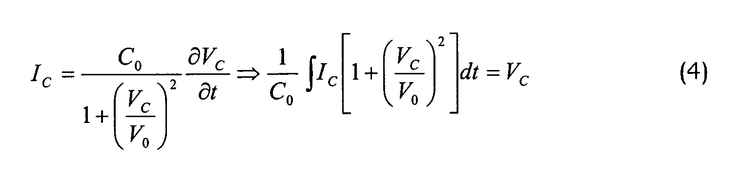
- the differential input voltage Vin+, Vin- corresponds to current Ic of Relation (4)
- the differential output voltage Vout+, Vout- corresponds to voltage Vc of the same Relation (4).
- the integrator pair 2 and 3 basically simulate the frequency performance of a capacitance C in the scale network of Figure 1.
- non-linear inductor L may be implemented through an identical integrator pair design.
- the differential input voltage Vin+, Vin- corresponds to voltage V1 of the inductor
- the differential output voltage Vout+, Vout- corresponds to current I1.
- the device 1 of this invention has, therefore, no integrated inductors, so that the circuit complexity and overall occupied area of the device can be minimized.
- Figure 4 schematically shows in deeper circuit detail the structure of device 1.
- both the first 2 and the second 3 integrator are formed with mixed bipolar-MOS technology by means of bipolar transistor differential cells biased by MOS circuit portions.
- the first integrator 2 comprises a differential cell having a double pair of transistors, Q1, Q2 and Q3, Q4, which is associated with the differential inputs A, and B.
- a bias circuit portion comprising MOS transistors M1,..., M6, is arranged to couple the differential cell with the supply voltage references Vdd and the bias voltage and current references I1 and V1.
- the transistors Q5, Q6 and Q7 diode configurated, couple the outputs U1, U2 of the first integrator 2 to ground.
- the outputs U1, U2 of the integrator 2 are connected to the respective inputs A2, B2 of the second integrator 3, the latter showing a differential cell structure of bipolar transistors with a double pair of input transistors Q8, Q9 and Q10, Q11.
- a bias circuit portion comprised of MOS transistors M7, M8, M9 and M10 couples the differential cell of integrator 3.
- a feedback block 4 connects the outputs O1, O2 of the second integrator 3 to the bias circuit portion in order to provide a voltage reference CMFB_ref for the transistor pair M7, M9.
- a capacitance with value Co/2 is inserted across the outputs O1 and O2.
- the device 1 allows the performance of one of the non-linear components of the scale network of Figure 1, both the capacitive component C and the inductive component L, to be emulated.
- the scale network structure can be reconstructed by using a plurality of suitably interconnected devices 1.
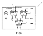
- Shown in Figure 5 is an exemplary portion of a scale network realised by connecting several devices 1 together, which are similar to the device described hereinabove.
- Figure 5 shows a first device 1, emulating a first inductor L1, as being connected to the voltage generator Vo at the first differential input A.
- the output O1 is connected to ground, and the output O2 is connected to the differential input A of a second device 1 emulating the capacitor C1.
- the output O2 of the second device emulating C1 is connected to the differential input B of the first device emulating L1.
- the output O1 of the second emulating C1 is connected to the differential input A of a third device 1 emulating a second inductor L2 in the scale network.
- the output O1 of the third device emulating L2 is connected to the differential input B of the second device emulating C1, and so on.
- a non-linear scale network can be implemented with at least twenty LC elements, without using integrated inductors.
- the network implemented with a cascade of devices 1 according to the invention has shown to have excellent characteristics of frequency response.
- the total circuit area occupied by the cascade of devices 1 is smaller than that required by conventional designs.
- non-linear scale network of the invention allows a cascade connection of many more elements than in conventional designs.
Landscapes
- Physics & Mathematics (AREA)
- Nonlinear Science (AREA)
- Networks Using Active Elements (AREA)
- Amplifiers (AREA)
Abstract
Description

Claims (8)
- A circuit device (1) for realising a non-linear reactive elements scale network, wherein the non-linear elements of the network are pairs of inductive (L) and capacitive (C) components cascade connected between a pair of input terminals and a pair of output terminals, characterised in that each component (L,C) of the network is formed by cascade connecting a first (2) and a second (3) transconductance (Gm1,Gm2) integrator with each other.
- A device according to Claim 1, characterised in that each integrator comprises a bipolar transistor input circuit portion and a MOS transistor bias circuit portion, and that the outputs of the second integrator (3) are feedback connected to the bias circuit portion of the same integrator through a feedback block (4).
- A device according to Claim 2, characterised in that said feedback block (4) provides a voltage reference (CMFB_ref) for said bias circuit portion.
- A device according to Claim 1, characterised in that the outputs (U1,U2) of the first integrator (2) connected to the inputs (A2,B2) of the second integrator (3) are further coupled to ground by respective diodes (Q5,Q6).
- A device according to Claim 1, characterised in that it comprises differential outputs (O1,O2) respectively coupled to ground through a stabilization capacitance (Co).
- A device according to Claim 1, characterised in that the first (2) and the second (3) integrator have the same transconductance (Gm1,Gm2).
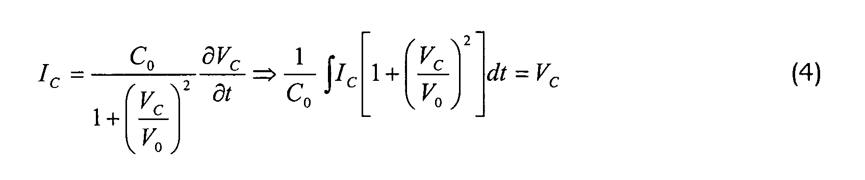
- A device according to Claim 1, characterised in that each pair of integrators (2,3) implements the following relation, in order to emulate a capacitor (C), or a similar relation with L indexes in order to emulate an inductor (L):
- A scale network (5) of LC non-linear elements, characterised in that it comprises at least twenty devices (1) as claimed in Claim 1.
Priority Applications (3)
| Application Number | Priority Date | Filing Date | Title |
|---|---|---|---|
| DE60217881T DE60217881D1 (en) | 2002-11-28 | 2002-11-28 | Circuit device for producing a non-linear scaling network with reactive elements |
| EP02425734A EP1424773B1 (en) | 2002-11-28 | 2002-11-28 | Circuit device for realising a non-linear reactive elements scale network |
| US10/705,765 US7042304B2 (en) | 2002-11-28 | 2003-11-10 | Circuit device for realizing a non-linear reactive elements scale network |
Applications Claiming Priority (1)
| Application Number | Priority Date | Filing Date | Title |
|---|---|---|---|
| EP02425734A EP1424773B1 (en) | 2002-11-28 | 2002-11-28 | Circuit device for realising a non-linear reactive elements scale network |
Publications (2)
| Publication Number | Publication Date |
|---|---|
| EP1424773A1 true EP1424773A1 (en) | 2004-06-02 |
| EP1424773B1 EP1424773B1 (en) | 2007-01-24 |
Family
ID=32241387
Family Applications (1)
| Application Number | Title | Priority Date | Filing Date |
|---|---|---|---|
| EP02425734A Expired - Lifetime EP1424773B1 (en) | 2002-11-28 | 2002-11-28 | Circuit device for realising a non-linear reactive elements scale network |
Country Status (3)
| Country | Link |
|---|---|
| US (1) | US7042304B2 (en) |
| EP (1) | EP1424773B1 (en) |
| DE (1) | DE60217881D1 (en) |
Families Citing this family (4)
| Publication number | Priority date | Publication date | Assignee | Title |
|---|---|---|---|---|
| TWI336468B (en) * | 2005-03-02 | 2011-01-21 | Ind Tech Res Inst | Asymmetry compensator for partial response maximum likelihood (prml) decoder |
| US7969222B2 (en) * | 2005-09-16 | 2011-06-28 | Broadcom Corporation | Method and system for DC offset correction loop for a mobile digital cellular television environment |
| US7679443B2 (en) * | 2006-08-31 | 2010-03-16 | Texas Instruments Incorporated | System and method for common mode translation |
| US10033351B2 (en) * | 2014-12-08 | 2018-07-24 | Avago Technologies General Ip (Singapore) Pte. Ltd. | Long-distance high-speed data and clock transmission |
Citations (1)
| Publication number | Priority date | Publication date | Assignee | Title |
|---|---|---|---|---|
| US20020011895A1 (en) * | 1999-05-14 | 2002-01-31 | Timothy C. Kuo | Method and arrangement for filtering with common mode feedback for low power consumption |
Family Cites Families (16)
| Publication number | Priority date | Publication date | Assignee | Title |
|---|---|---|---|---|
| US4839542A (en) * | 1984-08-21 | 1989-06-13 | General Datacomm Industries, Inc. | Active transconductance filter device |
| GB8513329D0 (en) * | 1985-05-28 | 1985-07-03 | Secr Defence | Transconductors |
| US4855696A (en) * | 1987-12-09 | 1989-08-08 | Hewlett-Packard | Pulse compressor |
| NL9002154A (en) * | 1990-10-04 | 1992-05-06 | Philips Nv | COMPANDING POWER MODE TRANSCONDUCTOR-C INTEGRATOR. |
| IT1252392B (en) * | 1991-11-13 | 1995-06-12 | Sgs Thomson Microelectronics | TRANSCONDUCTOR STAGE PERFECTED FOR HIGH FREQUENCY FILTERS |
| US5804921A (en) * | 1994-02-09 | 1998-09-08 | The Regents Of The University Of California | Soliton quenching NLTL impulse circuit with a pulse forming network at the output |
| JP3361021B2 (en) * | 1996-12-16 | 2003-01-07 | 株式会社東芝 | Filter circuit |
| US6069522A (en) * | 1997-02-03 | 2000-05-30 | Texas Instruments Incorporated | Circuitry and method for providing boost and asymmetry in a continuous-time filter |
| US6317016B1 (en) * | 1999-05-14 | 2001-11-13 | Koninklijke Philips Electronics | Method and arrangement for gyration filtering with low power consumption |
| CA2298310C (en) * | 2000-02-09 | 2003-07-29 | James A. Cherry | Low-voltage transconductance amplifier/filters |
| US6614609B1 (en) * | 2000-03-08 | 2003-09-02 | Cirrus Logic, Inc. | Gray code detection for a disk drive system |
| JP2001345696A (en) * | 2000-05-30 | 2001-12-14 | Oki Electric Ind Co Ltd | Tuning circuit |
| US6580326B2 (en) * | 2001-05-25 | 2003-06-17 | Infineon Technologies North America Corp. | High-bandwidth low-voltage gain cell and voltage follower having an enhanced transconductance |
| US6690243B1 (en) * | 2001-06-07 | 2004-02-10 | Cypress Semiconductor Corp. | Multi-phase voltage-controlled oscillator at modulated, operating frequency |
| US6697001B1 (en) * | 2002-12-19 | 2004-02-24 | Motorola, Inc. | Continuous-time sigma-delta modulator with discrete time common-mode feedback |
| US6784698B1 (en) * | 2003-06-11 | 2004-08-31 | Agere Systems Inc. | Sense amplifier with improved common mode rejection |
-
2002
- 2002-11-28 DE DE60217881T patent/DE60217881D1/en not_active Expired - Lifetime
- 2002-11-28 EP EP02425734A patent/EP1424773B1/en not_active Expired - Lifetime
-
2003
- 2003-11-10 US US10/705,765 patent/US7042304B2/en not_active Expired - Lifetime
Patent Citations (1)
| Publication number | Priority date | Publication date | Assignee | Title |
|---|---|---|---|---|
| US20020011895A1 (en) * | 1999-05-14 | 2002-01-31 | Timothy C. Kuo | Method and arrangement for filtering with common mode feedback for low power consumption |
Non-Patent Citations (1)
| Title |
|---|
| D.T. BICKLEY: "design of nonlinear networks using gyrators", ELECTRONICS LETTERS., vol. 3, no. 11, November 1967 (1967-11-01), IEE STEVENAGE., GB, pages 519 - 521, XP002241390, ISSN: 0013-5194 * |
Also Published As
| Publication number | Publication date |
|---|---|
| US20040150456A1 (en) | 2004-08-05 |
| DE60217881D1 (en) | 2007-03-15 |
| EP1424773B1 (en) | 2007-01-24 |
| US7042304B2 (en) | 2006-05-09 |
Similar Documents
| Publication | Publication Date | Title |
|---|---|---|
| US7535289B2 (en) | Integrated RC filter | |
| Minaei et al. | A new CMOS electronically tunable current conveyor and its application to current-mode filters | |
| Alzaher et al. | A CMOS fully balanced second-generation current conveyor | |
| EP0608886B1 (en) | Differential amplifier circuit having a driver with square-law characteristic | |
| US6664854B2 (en) | Base band filter including a semiconductor integrated circuit | |
| EP1444777B1 (en) | A power amplifier module with distortion compensation | |
| US6919768B2 (en) | Balanced amplifier and filter using the same | |
| US20050134379A1 (en) | Multi-port cross-connected multi-level cascode differential amplifier | |
| Ferri et al. | High-valued passive element simulation using low-voltage low-power current conveyors for fully integrated applications | |
| CN117914275A (en) | Push-pull operational amplifier circuit with feed-forward structure | |
| EP1424773B1 (en) | Circuit device for realising a non-linear reactive elements scale network | |
| US6433626B1 (en) | Current-mode filter with complex zeros | |
| US6359503B1 (en) | Basic cell for programmable analog time-continuous filter | |
| US10382011B2 (en) | Grounded capacitance multipliers with electronic tuning possibility using single current feedback amplifier | |
| Chaichana et al. | Current-mode MISO filter using CCCDTAs and grounded capacitors | |
| US9160309B2 (en) | Area efficient baseband filter | |
| US20070222510A1 (en) | System and method for operating a feedback network | |
| US7180357B2 (en) | Operational amplifier integrator | |
| Prodanov et al. | A differential active load and its applications in CMOS analog circuit designs | |
| US6958650B1 (en) | Push-pull buffer/amplifier | |
| US5973539A (en) | Mixer circuit for mixing two signals having mutually different frequencies | |
| US6239653B1 (en) | Biquadratic basic cell for programmable analog time-continuous filter | |
| RU2404452C2 (en) | Current multiplier based on root current-voltage characteristic of mos transistor | |
| Bayard | CFOA based inverting amplifier bandwidth enhancement | |
| Pandey et al. | SIMO Transadmittance Mode Active-C Universal Filter. |
Legal Events
| Date | Code | Title | Description |
|---|---|---|---|
| PUAI | Public reference made under article 153(3) epc to a published international application that has entered the european phase |
Free format text: ORIGINAL CODE: 0009012 |
|
| AK | Designated contracting states |
Kind code of ref document: A1 Designated state(s): AT BE BG CH CY CZ DE DK EE ES FI FR GB GR IE IT LI LU MC NL PT SE SK TR |
|
| AX | Request for extension of the european patent |
Extension state: AL LT LV MK RO SI |
|
| 17P | Request for examination filed |
Effective date: 20041130 |
|
| AKX | Designation fees paid |
Designated state(s): DE FR GB IT |
|
| GRAP | Despatch of communication of intention to grant a patent |
Free format text: ORIGINAL CODE: EPIDOSNIGR1 |
|
| GRAS | Grant fee paid |
Free format text: ORIGINAL CODE: EPIDOSNIGR3 |
|
| GRAA | (expected) grant |
Free format text: ORIGINAL CODE: 0009210 |
|
| AK | Designated contracting states |
Kind code of ref document: B1 Designated state(s): DE FR GB IT |
|
| REG | Reference to a national code |
Ref country code: GB Ref legal event code: FG4D |
|
| REF | Corresponds to: |
Ref document number: 60217881 Country of ref document: DE Date of ref document: 20070315 Kind code of ref document: P |
|
| ET | Fr: translation filed | ||
| PLBE | No opposition filed within time limit |
Free format text: ORIGINAL CODE: 0009261 |
|
| STAA | Information on the status of an ep patent application or granted ep patent |
Free format text: STATUS: NO OPPOSITION FILED WITHIN TIME LIMIT |
|
| 26N | No opposition filed |
Effective date: 20071025 |
|
| PG25 | Lapsed in a contracting state [announced via postgrant information from national office to epo] |
Ref country code: DE Free format text: LAPSE BECAUSE OF FAILURE TO SUBMIT A TRANSLATION OF THE DESCRIPTION OR TO PAY THE FEE WITHIN THE PRESCRIBED TIME-LIMIT Effective date: 20070425 |
|
| REG | Reference to a national code |
Ref country code: FR Ref legal event code: ST Effective date: 20080930 |
|
| PG25 | Lapsed in a contracting state [announced via postgrant information from national office to epo] |
Ref country code: FR Free format text: LAPSE BECAUSE OF NON-PAYMENT OF DUE FEES Effective date: 20071130 |
|
| PGFP | Annual fee paid to national office [announced via postgrant information from national office to epo] |
Ref country code: GB Payment date: 20101026 Year of fee payment: 9 Ref country code: IT Payment date: 20101105 Year of fee payment: 9 |
|
| GBPC | Gb: european patent ceased through non-payment of renewal fee |
Effective date: 20121128 |
|
| PG25 | Lapsed in a contracting state [announced via postgrant information from national office to epo] |
Ref country code: IT Free format text: LAPSE BECAUSE OF NON-PAYMENT OF DUE FEES Effective date: 20121128 |
|
| PG25 | Lapsed in a contracting state [announced via postgrant information from national office to epo] |
Ref country code: GB Free format text: LAPSE BECAUSE OF NON-PAYMENT OF DUE FEES Effective date: 20121128 |