EP1424737A2 - Actuator and method of making the same - Google Patents
Actuator and method of making the same Download PDFInfo
- Publication number
- EP1424737A2 EP1424737A2 EP03027346A EP03027346A EP1424737A2 EP 1424737 A2 EP1424737 A2 EP 1424737A2 EP 03027346 A EP03027346 A EP 03027346A EP 03027346 A EP03027346 A EP 03027346A EP 1424737 A2 EP1424737 A2 EP 1424737A2
- Authority
- EP
- European Patent Office
- Prior art keywords
- silicon
- piezoelectric
- electrode
- actuator
- arm
- Prior art date
- Legal status (The legal status is an assumption and is not a legal conclusion. Google has not performed a legal analysis and makes no representation as to the accuracy of the status listed.)
- Granted
Links
Images



Classifications
-
- H—ELECTRICITY
- H10—SEMICONDUCTOR DEVICES; ELECTRIC SOLID-STATE DEVICES NOT OTHERWISE PROVIDED FOR
- H10N—ELECTRIC SOLID-STATE DEVICES NOT OTHERWISE PROVIDED FOR
- H10N30/00—Piezoelectric or electrostrictive devices
- H10N30/80—Constructional details
-
- G—PHYSICS
- G11—INFORMATION STORAGE
- G11B—INFORMATION STORAGE BASED ON RELATIVE MOVEMENT BETWEEN RECORD CARRIER AND TRANSDUCER
- G11B5/00—Recording by magnetisation or demagnetisation of a record carrier; Reproducing by magnetic means; Record carriers therefor
- G11B5/48—Disposition or mounting of heads or head supports relative to record carriers ; arrangements of heads, e.g. for scanning the record carrier to increase the relative speed
- G11B5/54—Disposition or mounting of heads or head supports relative to record carriers ; arrangements of heads, e.g. for scanning the record carrier to increase the relative speed with provision for moving the head into or out of its operative position or across tracks
- G11B5/55—Track change, selection or acquisition by displacement of the head
- G11B5/5521—Track change, selection or acquisition by displacement of the head across disk tracks
- G11B5/5552—Track change, selection or acquisition by displacement of the head across disk tracks using fine positioning means for track acquisition separate from the coarse (e.g. track changing) positioning means
-
- H—ELECTRICITY
- H10—SEMICONDUCTOR DEVICES; ELECTRIC SOLID-STATE DEVICES NOT OTHERWISE PROVIDED FOR
- H10N—ELECTRIC SOLID-STATE DEVICES NOT OTHERWISE PROVIDED FOR
- H10N30/00—Piezoelectric or electrostrictive devices
- H10N30/01—Manufacture or treatment
- H10N30/03—Assembling devices that include piezoelectric or electrostrictive parts
-
- H—ELECTRICITY
- H10—SEMICONDUCTOR DEVICES; ELECTRIC SOLID-STATE DEVICES NOT OTHERWISE PROVIDED FOR
- H10N—ELECTRIC SOLID-STATE DEVICES NOT OTHERWISE PROVIDED FOR
- H10N30/00—Piezoelectric or electrostrictive devices
- H10N30/01—Manufacture or treatment
- H10N30/07—Forming of piezoelectric or electrostrictive parts or bodies on an electrical element or another base
- H10N30/072—Forming of piezoelectric or electrostrictive parts or bodies on an electrical element or another base by laminating or bonding of piezoelectric or electrostrictive bodies
- H10N30/073—Forming of piezoelectric or electrostrictive parts or bodies on an electrical element or another base by laminating or bonding of piezoelectric or electrostrictive bodies by fusion of metals or by adhesives
-
- H—ELECTRICITY
- H10—SEMICONDUCTOR DEVICES; ELECTRIC SOLID-STATE DEVICES NOT OTHERWISE PROVIDED FOR
- H10N—ELECTRIC SOLID-STATE DEVICES NOT OTHERWISE PROVIDED FOR
- H10N30/00—Piezoelectric or electrostrictive devices
- H10N30/20—Piezoelectric or electrostrictive devices with electrical input and mechanical output, e.g. functioning as actuators or vibrators
- H10N30/204—Piezoelectric or electrostrictive devices with electrical input and mechanical output, e.g. functioning as actuators or vibrators using bending displacement, e.g. unimorph, bimorph or multimorph cantilever or membrane benders
- H10N30/2041—Beam type
- H10N30/2042—Cantilevers, i.e. having one fixed end
- H10N30/2043—Cantilevers, i.e. having one fixed end connected at their free ends, e.g. parallelogram type
Definitions
- the present invention relates to an actuator utilizing a piezoelectric device, and a method of making the same.
- the present invention relates to an actuator employed for controlling the position of a magnetic head in a magnetic recording apparatus, and a method of making the same.
- Such an actuator is disclosed, for example, in the Japanese Patent Application Laid-open No. 2002-26411 and No. 2002-289936.
- a flat laminated piezoelectric device having an inner electrode is attached to each of a pair of flat arms opposing each other.
- a pair of electrodes for applying a voltage to the piezoelectric device are provided on the surface opposite from the surface facing the arm in the piezoelectric device, whereas respective leads are attached to the pair of electrodes.
- the actuator in accordance with the present invention comprises an insulating substrate; a pair of silicon arms, doped with an impurity, having respective one end parts connected to both end faces of the insulating substrate; a piezoelectric part formed on a surface opposite from the surface connected to the insulating substrate in each silicon arm; and a first electrode formed on a surface opposite from the surface opposing the silicon arm in each piezoelectric part.
- a pair of silicon arms having lowered their resistance by doping with an impurity are connected to each other by way of an insulating substrate.
- Each silicon arm has a predetermined surface formed with a piezoelectric part, whereas the piezoelectric part has a predetermined surface formed with a first electrode. Therefore, when one of a pair of leads is attached to the first electrode while the other is attached to the silicon arm, and a voltage is applied between the pair of leads, the piezoelectric part is driven.
- the lead can be attached to the silicon arm at any position thereon. Hence, the lead can be attached to appropriately selected positions and surfaces where the lead is easily attachable. As a consequence, leads can be attached to this actuator more easily than to the conventional actuator.
- the actuator further comprises a second electrode formed on the surface formed with the piezoelectric part in the silicon arm. Since the first and second electrodes are oriented in the same direction, it becomes easier to attach leads to the respective electrodes in this case.
- the insulating substrate is constituted by glass.
- anode bonding which allows bonding at a relatively low temperature can be used for connecting the insulating substrate to the silicon arms, and the insulating substrate can easily be shaped by etching.
- the piezoelectric part may be a single-layer piezoelectric film, or have a laminate structure in which piezoelectric and electrode films are alternately laminated.
- the piezoelectric film is constituted by PZT.
- the first electrode has a multilayer structure, in which the topmost layer is constituted by Au or Pt. This can significantly restrain the piezoelectric part from being eroded by an etchant utilized for making the actuator.
- the method of making an actuator in accordance with the present invention comprises the steps of forming a piezoelectric film pattern on one surface each of two silicon substrates doped with an impurity; forming an electrode film on the piezoelectric film pattern; bonding the two silicon substrates, each formed with the piezoelectric film pattern and electrode film, to both sides of an insulating substrate, respectively, such that the piezoelectric film patterns are oriented outward; cutting a block having a predetermined form from a laminated substrate constitutedby the two silicon substrates and insulating substrate laminated together; and forming a silicon arm by cutting the block after partly removing the insulating substrate in the block on one side.
- two silicon substrates having lowered their resistance by doping with an impurity are connected to each other by way of an insulating substrate.
- Each silicon substrate is formed with a piezoelectric film pattern, whereas an electrode film is formed on the piezoelectric film pattern. Therefore, when one of apair of leads is attached to an electrode corresponding to the electrode film while the other is attached to a silicon arm in the actuator made by using this method, and a voltage is applied between the pair of leads, a piezoelectric part is driven.
- the lead can be attached to the silicon arm at any position thereon. Hence, the lead can be attached to appropriately selected positions and surfaces where the lead is easily attachable. As a consequence, leads can be attached to this actuator more easily than to the conventional actuator.
- the method further comprises the step of forming an electrode pattern on the silicon substrate.
- the electrode formed on the piezoelectric film and the electrode of the electrode pattern are oriented in the same direction, which makes it easier to attach leads to the respective electrodes.
- the insulating substrate is constituted by glass.
- anode bonding which allows bonding at a relatively low temperature can be used for connecting the insulating substrate to the silicon substrates, and the insulating substrate can easily be shaped by etching.
- the piezoelectric film pattern is constituted by PZT.
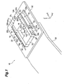
- Fig. 1 is a schematic perspective view showing the actuator in accordance with a first embodiment of the present invention.
- the actuator 10 in accordance with the first embodiment of the present invention is an actuator for HDD servo control, and displaces a head slider (hereinafter referred to as "slider") SL.
- the slider SL comprises a thin-film magnetic head H, which reads magnetic recording information from hard disks and records magnetic recording information onto hard disks.
- the slider SL has a substantially rectangular parallelepiped form, whose upper face in Fig. 1 is an air bearing surface facing a hard disk.
- the slider SL in Fig. 1 is illustrated schematically, while omitting a slider rail for adjusting the amount of levitation from the hard disk, etc.
- the actuator 10 comprises a glass substrate (insulating substrate) 12 formed like a rectangular plate; a pair of silicon arms 14, 14, each formed like a rectangular column; and respective arm drivers 16 and thin-film electrodes (second electrodes or electrodes for outer connections) 18 attached to the silicon arms 14, 14.
- the actuator 10 is mounted to a suspension arm 30 of a hard disk drive.
- the suspension arm 30 has a leading end provided with a gimbal 32, and is driven by a voice coil motor. More specifically, the actuator 10 is bonded and secured to a tongue 32a of the gimbal 32. Since the silicon arms 14, 14 are required to swing, an adhesive for securing the actuator 10 to the gimbal 32 is applied to only the glass substrate 12.
- Each silicon arm 14 is constituted by single-crystal silicon doped with impurities for lowering its resistance, and exhibits a resistivity of 1 ⁇ cm or less.
- Single-crystal silicon employed as a material for the silicon arm 14 is excellent as an elastic material, since it does not plastically deform within the temperature range in which the hard disk drive is used. Also, it has a high mechanical strength with less crystal defects, thereby enabling high-precision position control.
- any of donors such as phosphorus and acceptors such as aluminum and boron can be employed.
- the two silicon arms 14, 14 extend in parallel with each other, while having respective end faces 14a anodicallybonded to opposing end faces of the glass substrate 12. Namely, a substantially U-shaped integral structure in which the glass substrate 12 supports a pair of silicon arms 14, 14 is formed.
- X and Y directions directions in which the silicon arms 14, 14 extend and align
- Z direction a direction orthogonal to the X and Y directions
- Each arm driver 16 is formed on a surface 24b opposite from the surface 24a bonded to the glass substrate 12 in the respective silicon arm 14.
- the arm driver 16 extends in one direction like a rectangular plate, and is attached to the silicon arm 14 such that its longitudinal direction extends along the longitudinal direction (depicted X direction) of the silicon arm 14.
- Each thin-film electrode 18 is also formed like a substantially rectangular plate on the surface 24b opposite from the surface 24a bonded to the glass substrate 12 in the respective arm 14.
- the slider SL is secured to the inner side face 24a (surface bonded to the glass substrate 12) of each silicon arm 14 with an adhesive.
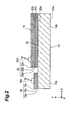
- FIG. 2 is a sectional view of the silicon arm 14 taken along the line II-II of Fig. 1.
- the arm driver 16 is formed in a partial region of the surface 24b of the silicon arm 14, and is constituted by a piezoelectric part 20 and a thin-film electrode (first electrode) 22.
- the piezoelectric part 20 is a single-layer piezoelectric film constituted by PZT (a mixture of lead zirconate and lead titanate).
- the thin-film electrode 22 is laminated on a surface 20b opposite from the surface 20a bonded to (opposing) the silicon arm 14 in the piezoelectric part 20.
- the thin-film electrode 22 has a three-layer structure in which a Cr layer 22a, an Ni layer 22b, and an Au layer 22c are laminated in this order from the side closer to the piezoelectric part 20.
- the thin-film electrode 18 is formed on the surface 24b on one end part 14a side of the silicon arm 14 so as not to overlap the region formed with the arm driver 16.
- the thin-film electrode 18 has a three-layer structure (constituted by a Cr layer 18a, an Ni layer 18b, and an Au layer 18c successively from the side closer to the silicon arm 14).
- the actuator 10 can control the position of the slider SL, and finely fluctuate the slider SL at a level which cannot be realized by the cooperation of a voice coil motor and suspension arms. Since the arm driver 16 formed like a rectangular plate is attached to the silicon arm 14 so as to have a longitudinal direction extending along the longitudinal direction of the silicon arm 14, displacements of the arm driver 16 can effectively be transmitted to the silicon arm 14, whereby the silicon arm 14 can be controlled with high precision.
- each silicon arm 14 having lowered its resistance by doping with impurities is utilized as a conductive path for applying a voltage to the piezoelectric part 20. Since a pair of silicon arms 14, 14 are connected to each other by way of an insulating glass substrate, each silicon arm 14 can be energized regardless of whether the other silicon arm 14 is energized or not.
- the thin-film electrode 22 Formed on the upper face 20b of the piezoelectric part 20 is the thin-film electrode 22 to which one bonding wire 22A in the pair of bonding wires 18A, 22A for applying a voltage to the piezoelectric part 20 is attached.
- a voltage can be applied to the piezoelectric part 20 regardless of where the other bonding wire 18A in the pair of bonding wires 18A, 22A is attached to the silicon arm 14.
- positions and surfaces where the bonding wire 18A is easily attachable can be selected as appropriate, so as to attach the bonding wire 18A to the silicon arm 14. Therefore, the couple of bonding wires 18A, 22Acanbe attached more easily to this actuator than to the conventional actuator.
- the electrically conductive silicon arm 14 is utilized as a conductor in contact with one side of the piezoelectric part 20, a wiring structure for supplying power to the piezoelectric part 20 is simplified.
- the thin-film electrode 18 When attaching the bonding wire 18A to the silicon arm 14 by way of the thin-film electrode 18, the thin-film electrode 18 is formed on the surface 20a formed with the arm driver 16 as mentioned above. Since the thin-film electrodes 18 and 22 are oriented in the same direction (Y direction in Figs. 1 and 2), the bonding wires 18A, 22A can easily be attached thereto along the Y direction.
- FIGs. 3A to 3E are schematic views showing a procedure of making the actuator 10 in accordance with the first embodiment of the present invention.
- a disk-shaped glass substrate (insulating substrate) 40 to become a glass substrate 12 is prepared, and its front and rear faces are ground (see Fig. 3A).
- two single-crystal silicon substrates 42 are bonded to the ground front and rear faces, respectively, so as to form a laminated substrate 44 (see Fig. 3B).
- Each of these silicon substrates 42 has a resistivity of 1 ⁇ cm or less as a result of doping with impurities.
- the glass substrate 40 and the silicon substrates 42 are anodically bonded to each other.
- FIGs. 4A to 4H are schematic sectional views showing a procedure of forming the piezoelectric film pattern and electrode pattern onto the silicon substrate in a region corresponding to one actuator.
- a silicon substrate 42 doped with impurities is prepared (see Fig. 4A), and one surface 42b thereof is formed with a mask layer 46 made of a film of SiO 2 or PSG (phosphorus-doped glass) to become a sacrificial layer (see Fig. 4B).
- a mask layer 46 made of a film of SiO 2 or PSG (phosphorus-doped glass) to become a sacrificial layer.
- the part of mask layer 46 corresponding to the region to be formed with the piezoelectric part 20 is etched away with HF or bufferedHF.
- a piezoelectric film 48 made of PZT is formed.
- sol-gel method ion beam sputtering, RF magnetron sputtering, DC magnetron sputtering, MOCVD, PLD, hydrothermal synthesis, electrophoresis, and the like can be utilized.
- the piezoelectric film 48 is also formed on the mask layer 46, the latter is lifted off, whereby only the piezoelectric film (piezoelectric film pattern) 49 directly formed on the surface 42b of the silicon substrate 42 remains as shown in the Fig. 4E.
- a ⁇ 100>-oriented Pt film may be formed on the surface of the silicon substrate 42 as appropriate before forming the piezoelectric film 48 on the silicon substrate 42.
- a liftoff resist layer 50 higher than the piezoelectric film 48 is formed (patterned) in an area between the respective regions to be formed with the thin-film electrodes 18 and 22.
- a Cr layer 52, an Ni layer 54, and an Au layer 56 are successively formed by a thin-film forming technique such as sputtering, thus yielding an electrode film 58 having a three-layer structure.
- the liftoff resist layer 50 is lifted off, thus forming an electrode film (electrode pattern) 58A to become the thin-film electrode 18 laminated on the silicon substrate 42 and an electrode film 58B to become the thin-film electrode 22 laminated on the piezoelectric film pattern 49 (see Fig. 4H).
- Each of the two silicon substrates 42 shown in Fig. 3B is formed with the piezoelectric film pattern 49 in which the electrode films 58B are laminated and the electrode pattern 58A in each area to become a silicon arm 14.
- formed patterns are arranged like grids.
- the two silicon substrates 42 are bonded to both sides of the glass substrate 40, respectively, such that the surfaces 42b formed with the piezoelectric film pattern 49 and electrode pattern 58A are oriented outward, thus yielding a disk-shaped laminated substrate 44.
- a block 60 in which a number of silicon arms are arranged in parallel with each other is cut out from the laminated substrate 44.
- the block 60 comprises a glass block 62 and a pair of silicon blocks 64, 64 disposed on both sides of the glass block 62, respectively.
- the glass block 62 in the block 60 is etched with HF or buffered HF while one glass block side face is masked, so as to leave longer silicon blocks 64 (series of silicon arms arranged in parallel) on both sides of the shortened glass block 62, respectively, as shown in Fig. 3D.
- the etched block 60 is cut at equally spaced intervals in surfaces perpendicular to the longitudinal direction thereof, whereby the actuators 10 are obtained.
- the actuator 10 made by using a technique for bonding a plurality of substrates and a technique for forming thin films can easily be made smaller, and can respond to further reductions in the size of the slider SL.
- the glass substrate 40 can easilybe shaped by etching, the glass substrate 12 of the actuator 10 can easily be formed. Adjusting the etching time for the glass substrate 40 can easily regulate the length of silicon arms.
- the Au layer formed as the topmost layer of the electrode film 58 acts as a resist layer when etching the glass substrate 40. This can significantly restrain the thin-film electrodes 18, 22 and the piezoelectric part 20 from being eroded by the etchant, without separately forming a resist for etching. Furthermore, even when the topmost layer of the electrode film 58 is the Pt layer, the effect is similar to when Au forms the topmost layer.
- the laminated substrate in which the glass substrate 40 is held between the silicon substrates 42 is cut into a block 60 (silicon block 64/glass block 62/silicon block 64) in which a number of actuators 10 are arranged in parallel, and the glass block 62 corresponding to the glass substrate 12 is etched while in the block state, the glass substrate 12 is efficiently shaped, whereby the cost is cut down.
- Dicers, slicers, wire saws, lasers, and the like can be used for cutting out and severing the block 60.
- Each piezoelectric film 20 for driving the respective silicon arm 14 is a piezoelectric film and can directly be formed by using a conventional thin-film forming technique onto the silicon substrate 42 to become the silicon arm 14 as mentioned above, whereby operations of bonding the piezoelectric device and the like become unnecessary, and the mass-productivity of actuators improves.
- Such a piezoelectric film can be formed as a pattern by lifting off a sacrificial layer.
- a block 60 having a sandwich structure of silicon block 64/glass block 62/silicon block 64 is obtained. Changing the thickness of the silicon block 64 (i.e., silicon substrate 42) alters the rigidity of the silicon arm 14, whereby actuators having desirable amounts of displacement can be made.
- the arm driver 16 may have a laminate structure in which piezoelectric films and inner electrode films are alternately laminated.
- Such an arm driver with a laminated structure may be made by various procedures that utilize known thin film stacking techniques.
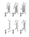
- Figs. 5A to 5F a procedure of making an arm driver having such a laminate structure will now be explained.
- Figs. 5A to 5F are schematic sectional views showing a procedure for forming an arm driver in another embodiment.
- a rectangular piezoelectric film pattern 49A made of PZT is formed on one surface 42b of a silicon substrate 42 doped with impurities (see Fig. 5A).
- the area excluding one end area 49a in the end parts longitudinally opposing each other in the piezoelectric film pattern 49A is formed with an electrode film 70 by vapor deposition, sputtering, or the like (see Fig. 5B).
- a piezoelectric film pattern 49B having the same crystal orientation as that of the piezoelectric film pattern 49A is formed on upper face regions of the piezoelectric film pattern 49A and electrode film 70 so as to expose the part of the electrode film 70 formed at the other end area in the end parts longitudinally opposing each other in the piezoelectric film pattern 49A (see Fig. 5C).
- the piezoelectric film pattern 49B is laminated on the piezoelectric film pattern 49A so as to keep the crystallinity.
- an electrode film 72 is formed on the piezoelectric film pattern 49B so as to expose the partial region 49b of the piezoelectric film pattern 49B without covering the exposed part of the electrode film 70 (see Fig. 5D) .
- the electrode film 72 is also formed on the side face of the piezoelectric film patterns 49A, 49B opposite from the side where the electrode film 70 is exposed, and is electrically connected to the silicon substrate 42.
- a piezoelectric film pattern 49C having the same crystal orientation as that of the piezoelectric film patterns 49A and 49B is formed so as to cover the upper face of the electrode film 72 and the exposed part of the piezoelectric film pattern 49B (see Fig. 5E).
- the piezoelectric film pattern 49C is laminated on the piezoelectric film pattern 49B so as to keep the crystallinity.
- an electrode film 74 is laminated so as to cover the piezoelectric film pattern 49C and the exposed part of the electrode film 70 (see Fig. 5F).
- the topmost electrode film 74 is a thin-film electrode which is substantially the same as the thin-film electrode 22 in the first embodiment, whereas the three layers of the piezoelectric film patterns 49A, 49B, 49C and the two layers of electrode films 70, 72 alternately interposed therebetween become a piezoelectric part substantially the same as the piezoelectric part 20 in the first embodiment.
- an actuator comprising arm drivers having a laminate structure is formed. Since the piezoelectric part has a laminate structure, thus formed actuator can attain a greater amount of displacement for each silicon arm 14 than does the actuator 10 in accordance with the first embodiment.
- an actuator may be made by utilizing a separately prepared arm driver.
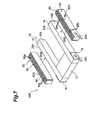
- a piezoelectric device 76 formed like a rectangular column in which a piezoelectric plate (piezoelectric part) 76A constituted by a piezoelectric material is held between a pair of electrode plates 76B, 76C on both sides may be used as an arm driver.
- Fig. 6 is a schematic perspective view showing an actuator in a mode using piezoelectric devices.
- a structure 78 constituted by silicon arms 14, a glass substrate 12, and thin-film electrodes 18 alone ismade.
- the piezoelectric device 76 is bonded and secured to each silicon arm 14 such that one electrode plate 76B of each piezoelectric device 76 and a surface 24b opposite from the bonding surface 24a between the silicon arm 14 and the glass substrate 12 oppose each other, and such that the longitudinal direction of the silicon arm 14 and the longitudinal direction of the piezoelectric device 76 align with each other.
- electrically conductive adhesives such as those of epoxy, silicone, and acrylic types, but insulating adhesives may also be used as long as they are partly applied so as to secure an electric connection between the silicon arm 14 and the electrode plate 76B.
- each silicon arm 14 having lowered its resistance by doping with impurities is utilized as a conductive path for applying a voltage to the respective piezoelectric plate 76A.
- a surface 76b opposite from the surface 76a facing the silicon arm 14 in the piezoelectric plate 76A is formed with an electrode plate (first electrode corresponding to the above-mentioned thin-film electrode 22) 76C to which one bonding wire 22A in a pair of bonding wires 18A, 22A for applying a voltage to the piezoelectric plate 76A is attached.
- a voltage can be applied to the piezoelectric plate 76A regardless of where the other bonding wire 18A in the pair of bonding wires 18A, 22A is attached to the silicon arm 14.
- the bonding wire 18A can be attached to the silicon arm 14 while appropriately selecting positions and surfaces where the bonding wire 18A is easily attachable.
- a pair of bonding wires 18A, 22A can be attached to this actuator more easily than to the conventional actuator.
- the piezoelectric device attached to the silicon arm 14 is not limited to the piezoelectric device 76 having a single layer of piezoelectric plate shown in the third embodiment, but may be a laminated piezoelectric device 80 in which a plurality of piezoelectric layers and inner electrodes are laminated as shown in Fig. 7.
- Fig. 7 is a schematic perspective view showing an actuator using piezoelectric devices in a mode different from that in Fig. 6.
- the actuator 10B in accordance with the fourth embodiment utilizes a piezoelectric device 80, in which a pair of outer electrode plates 82A, 82B each having an L-shaped cross section hold a laminated piezoelectric body (piezoelectric part) 84 therebetween, as an arm driver.
- the laminated piezoelectric body 84 is constituted by piezoelectric layers 86 and inner electrodes 88a, 88b which are alternately laminated. An end part of each inner electrode 88a is exposed at one end face of the laminated piezoelectric body 84 and is connected to the outer electrode 82B. On the other hand, an end part of each inner electrode 88b is exposed at the other end face of the laminated piezoelectric body 84 and is connected to the outer electrode plate 82A.
- Each piezoelectric device 80 is bonded and secured to the respective silicon arm 14 so as to have a longitudinal direction aligning with that of the piezoelectric device 76 such that one outer electrode plate 82B opposes the surface 24b opposite from the surface 24a bonded to the glass substrate 12 in the silicon arm 14.
- the other outer electrode plate 82A first electrode is not in contact with the silicon arm 14 but forms a gap therebetween.
- the bonding wire 18A can be attached to each silicon arm 14 while appropriately selecting positions and surfaces where the bonding wire 18A is easily attachable.
- a pair of bonding wires 18A, 22A can be attached to this actuator more easily than to the conventional actuator.
- the piezoelectric device 80 is of laminate type, the amount of displacement of each silicon arm 14 can be made greater than that in the actuator 10A having the piezoelectric device 76.
- the piezoelectric device not only the single-plate and laminate types, but those of bimorph type can also be utilized.
Landscapes
- Engineering & Computer Science (AREA)
- Manufacturing & Machinery (AREA)
- Moving Of The Head To Find And Align With The Track (AREA)
- Micromachines (AREA)
- General Electrical Machinery Utilizing Piezoelectricity, Electrostriction Or Magnetostriction (AREA)
- Adjustment Of The Magnetic Head Position Track Following On Tapes (AREA)
- Piezo-Electric Or Mechanical Vibrators, Or Delay Or Filter Circuits (AREA)
- Impact Printers (AREA)
Abstract
Description
Claims (11)
- An actuator comprising:an insulating substrate;a pair of silicon arms, doped with an impurity, having respective one end parts connected to both end faces of the insulating substrate;a piezoelectric part formed on a surface opposite from the surface connected to the insulating substrate in each silicon arm; anda first electrode formed on a surface opposite from the surface opposing the silicon arm in each piezoelectric part.
- An actuator according to claim 1, further comprising a second electrode formed on the surface formed with the piezoelectric part in the silicon arm.
- An actuator according to claim 1 or 2, wherein the insulating substrate is constituted by glass.
- An actuator according to one of claims 1 to 3, wherein the piezoelectric part is a single-layer piezoelectric film.
- An actuator according to one of claims 1 to 3, wherein the piezoelectric part has a laminate structure comprising alternately laminated piezoelectric and electrode films.
- An actuator according to claim 4 or 5, wherein the piezoelectric film is constituted by PZT.
- An actuator according to one of claims 1 to 6, wherein the first electrode comprises a multilayer structure including a topmost layer constituted by Au or Pt.
- A method of making an actuator, the method comprising the steps of:forming a piezoelectric film pattern on one surface each of two silicon substrates doped with an impurity;forming an electrode film on the piezoelectric film pattern;bonding the two silicon substrates, each formed with the piezoelectric film pattern and electrode film, to both sides of an insulating substrate, respectively, such that the piezoelectric film patterns are oriented outward;cutting a block having a predetermined form from a laminated substrate constituted by the two silicon substrates and insulating substrate laminated together; andforming a silicon arm by cutting the block after partly removing the insulating substrate in the block on one side.
- A method of making an actuator according to claim 8, further comprising the step of forming an electrode pattern on the silicon substrate.
- Amethod of making an actuator according to claim 8 or 9, wherein the insulating substrate is constituted by glass.
- A method of making an actuator according to one of claims 8 to 10, wherein the piezoelectric film pattern is constituted by PZT.
Applications Claiming Priority (4)
| Application Number | Priority Date | Filing Date | Title |
|---|---|---|---|
| JP2002345815 | 2002-11-28 | ||
| JP2002346476 | 2002-11-28 | ||
| JP2002346476 | 2002-11-28 | ||
| JP2002345815 | 2002-11-28 |
Publications (3)
| Publication Number | Publication Date |
|---|---|
| EP1424737A2 true EP1424737A2 (en) | 2004-06-02 |
| EP1424737A3 EP1424737A3 (en) | 2006-04-05 |
| EP1424737B1 EP1424737B1 (en) | 2007-01-17 |
Family
ID=32301863
Family Applications (2)
| Application Number | Title | Priority Date | Filing Date |
|---|---|---|---|
| EP03027346A Expired - Lifetime EP1424737B1 (en) | 2002-11-28 | 2003-11-26 | Actuator and method of making the same |
| EP03027347A Expired - Lifetime EP1424738B1 (en) | 2002-11-28 | 2003-11-26 | Actuator and method of making the same |
Family Applications After (1)
| Application Number | Title | Priority Date | Filing Date |
|---|---|---|---|
| EP03027347A Expired - Lifetime EP1424738B1 (en) | 2002-11-28 | 2003-11-26 | Actuator and method of making the same |
Country Status (5)
| Country | Link |
|---|---|
| US (2) | US7050271B2 (en) |
| EP (2) | EP1424737B1 (en) |
| KR (2) | KR20040047665A (en) |
| CN (2) | CN1319046C (en) |
| DE (2) | DE60311223T2 (en) |
Families Citing this family (25)
| Publication number | Priority date | Publication date | Assignee | Title |
|---|---|---|---|---|
| US7248444B1 (en) * | 2000-07-21 | 2007-07-24 | Lauer Mark A | Electromagnetic heads, flexures, gimbals and actuators formed on and from a wafer substrate |
| US7050271B2 (en) * | 2002-11-28 | 2006-05-23 | Tdk Corporation | Actuator having doped silicon arms and method of making the same |
| WO2005104257A1 (en) * | 2004-04-23 | 2005-11-03 | Agency For Science, Technology And Research | Micro-electromechanical device |
| US20060146448A1 (en) * | 2004-12-30 | 2006-07-06 | Gregory Tran | Method and apparatus for an actuator arm block including a crash stop stub in a hard disk drive |
| US7433159B2 (en) * | 2005-01-27 | 2008-10-07 | Sae Magnetics (H.K.) Ltd. | Micro-actuator unit, head gimbal assembly, and disk drive unit with vibration canceller |
| US7535680B2 (en) * | 2005-06-29 | 2009-05-19 | Sae Magnetics (H.K.) Ltd. | Micro-actuator with integrated trace and bonding pad support |
| US7411764B2 (en) * | 2005-09-30 | 2008-08-12 | Sae Magnetics (H.K.) Ltd. | Head gimbal assembly with precise positioning actuator for read/write head and disk drive device with the head gimbal assembly |
| JP2007144992A (en) * | 2005-10-28 | 2007-06-14 | Fujifilm Corp | Uneven structure and manufacturing method thereof, piezoelectric element, ink jet recording head, ink jet recording apparatus |
| US7518833B2 (en) * | 2005-11-15 | 2009-04-14 | Sae Magnetics H.K. Ltd. | Micro-actuator with electric spark preventing structure, HGA, and disk drive unit with the same, and manufacturing method thereof |
| US7796363B2 (en) * | 2006-05-25 | 2010-09-14 | Sae Magnetics (H.K.) Ltd. | PZT element, head gimbal assembly, and disk drive unit with same |
| US7855489B2 (en) * | 2007-01-31 | 2010-12-21 | Hitachi Global Storage Technologies, Netherlands, B.V. | Microactuator substrate |
| JP5268762B2 (en) * | 2009-04-20 | 2013-08-21 | 日本発條株式会社 | Piezoelectric actuator processing apparatus and piezoelectric actuator processing method |
| US20120140360A1 (en) * | 2010-12-07 | 2012-06-07 | John Contreras | Integrated lead suspension (ils) for use with a dual stage actuator (dsa) |
| US9759739B2 (en) | 2011-02-02 | 2017-09-12 | Honeywell International Inc. | MEMS vibrating-beam accelerometer with piezoelectric drive |
| US9190086B1 (en) | 2011-11-30 | 2015-11-17 | Magnecomp Corporation | GSA suspension having slider clearance for shock performance |
| US8879210B1 (en) | 2011-11-30 | 2014-11-04 | Magnecomp Corporation | DSA suspension with microactuators extending to gimbal through flexible connectors |
| US8947831B1 (en) | 2011-11-30 | 2015-02-03 | Magnecomp Corporation | GSA suspension with microactuators extending to gimbal through flexible connectors |
| US10607642B2 (en) | 2013-03-18 | 2020-03-31 | Magnecomp Corporation | Multi-layer PZT microactuator with active PZT constraining layers for a DSA suspension |
| US9741376B1 (en) | 2013-03-18 | 2017-08-22 | Magnecomp Corporation | Multi-layer PZT microactuator having a poled but inactive PZT constraining layer |
| US11205449B2 (en) | 2013-03-18 | 2021-12-21 | Magnecomp Corporation | Multi-layer PZT microacuator with active PZT constraining layers for a DSA suspension |
| US10128431B1 (en) | 2015-06-20 | 2018-11-13 | Magnecomp Corporation | Method of manufacturing a multi-layer PZT microactuator using wafer-level processing |
| CN108137379A (en) | 2015-10-02 | 2018-06-08 | 旭硝子株式会社 | Glass substrate, laminated substrate and laminated body |
| JP7051322B2 (en) * | 2016-08-03 | 2022-04-11 | マグネコンプ コーポレーション | Multilayer PZT microactuator with a polarized but inert PZT inhibitory layer |
| JP7626525B2 (en) * | 2016-12-29 | 2025-02-04 | ソニーグループ株式会社 | Actuator manufacturing method |
| JP2021144779A (en) * | 2020-03-13 | 2021-09-24 | 株式会社東芝 | Suspension assembly and disk device |
Family Cites Families (21)
| Publication number | Priority date | Publication date | Assignee | Title |
|---|---|---|---|---|
| US5438231A (en) * | 1993-08-23 | 1995-08-01 | Rockwell International Corporation | Thin film micromechanical resonator gyro |
| US5914801A (en) * | 1996-09-27 | 1999-06-22 | Mcnc | Microelectromechanical devices including rotating plates and related methods |
| US5903380A (en) * | 1997-05-01 | 1999-05-11 | Rockwell International Corp. | Micro-electromechanical (MEM) optical resonator and method |
| US6163434A (en) * | 1997-10-23 | 2000-12-19 | Seagate Technology Llc | Piezoresistive position sensors embedded in disc drive microactuator |
| US6239952B1 (en) * | 1997-12-04 | 2001-05-29 | Seagate Technology, Llc | Microactuator suspension with multiple “I” shaped microbeams |
| US6078473A (en) * | 1998-05-13 | 2000-06-20 | Seagate Technology, Inc. | Gimbal flexure for use with microactuator |
| JP3065611B1 (en) * | 1999-05-28 | 2000-07-17 | 三菱電機株式会社 | Micromirror device and manufacturing method thereof |
| JP4058223B2 (en) | 1999-10-01 | 2008-03-05 | 日本碍子株式会社 | Piezoelectric / electrostrictive device and manufacturing method thereof |
| JP2002026411A (en) | 1999-10-01 | 2002-01-25 | Ngk Insulators Ltd | Piezoelectric/electrostrictive device and manufacturing method thereof |
| WO2001075985A1 (en) * | 2000-03-30 | 2001-10-11 | Fujitsu Limited | Piezoelectric actuator, its manufacturing method, and ink-jet head comprising the same |
| US6453744B2 (en) * | 2000-05-10 | 2002-09-24 | Honeywell International, Inc. | Low radiation capture cross-section electrode material for prompt radiation environments |
| EP1306908A4 (en) | 2000-06-16 | 2006-10-04 | Ngk Insulators Ltd | Piezoelectric/electrostrictive device and method of producing the same |
| JP4007767B2 (en) | 2001-01-18 | 2007-11-14 | 日本碍子株式会社 | Piezoelectric / electrostrictive device and manufacturing method thereof |
| US6735004B1 (en) * | 2001-03-15 | 2004-05-11 | Nanogear, Inc. | Rotatable counterbalanced actuator |
| JP4033643B2 (en) | 2001-06-18 | 2008-01-16 | 日本碍子株式会社 | Piezoelectric / electrostrictive device and manufacturing method thereof |
| US20030022412A1 (en) * | 2001-07-25 | 2003-01-30 | Motorola, Inc. | Monolithic semiconductor-piezoelectric device structures and electroacoustic charge transport devices |
| JP4434537B2 (en) | 2001-08-27 | 2010-03-17 | パナソニック株式会社 | Piezoelectric functional parts |
| US6824278B2 (en) * | 2002-03-15 | 2004-11-30 | Memx, Inc. | Self-shadowing MEM structures |
| JP4100953B2 (en) * | 2002-04-18 | 2008-06-11 | キヤノン株式会社 | LAMINATE HAVING SINGLE CRYSTAL OXIDE CONDUCTOR ON Si SUBSTRATE, ACTUATOR USING SAME, INKJET HEAD, AND MANUFACTURING METHOD THEREOF |
| US7050271B2 (en) * | 2002-11-28 | 2006-05-23 | Tdk Corporation | Actuator having doped silicon arms and method of making the same |
| US7411339B2 (en) * | 2003-11-28 | 2008-08-12 | Seiko Epson Corporation | Manufacturing method of actuator device and liquid jet apparatus provided with actuator device formed by manufacturing method of the same |
-
2003
- 2003-11-25 US US10/720,142 patent/US7050271B2/en not_active Expired - Lifetime
- 2003-11-25 US US10/720,440 patent/US7119994B2/en not_active Expired - Fee Related
- 2003-11-26 KR KR1020030084580A patent/KR20040047665A/en not_active Withdrawn
- 2003-11-26 EP EP03027346A patent/EP1424737B1/en not_active Expired - Lifetime
- 2003-11-26 DE DE60311223T patent/DE60311223T2/en not_active Expired - Lifetime
- 2003-11-26 EP EP03027347A patent/EP1424738B1/en not_active Expired - Lifetime
- 2003-11-26 KR KR1020030084583A patent/KR20040047666A/en not_active Withdrawn
- 2003-11-26 DE DE60317156T patent/DE60317156T2/en not_active Expired - Lifetime
- 2003-11-28 CN CNB200310115769XA patent/CN1319046C/en not_active Expired - Fee Related
- 2003-11-28 CN CNB2003101157736A patent/CN1320525C/en not_active Expired - Fee Related
Also Published As
| Publication number | Publication date |
|---|---|
| US7119994B2 (en) | 2006-10-10 |
| CN1504998A (en) | 2004-06-16 |
| EP1424738B1 (en) | 2007-10-31 |
| CN1504999A (en) | 2004-06-16 |
| KR20040047666A (en) | 2004-06-05 |
| EP1424737A3 (en) | 2006-04-05 |
| US7050271B2 (en) | 2006-05-23 |
| DE60311223T2 (en) | 2007-05-10 |
| DE60317156T2 (en) | 2008-11-13 |
| CN1319046C (en) | 2007-05-30 |
| DE60317156D1 (en) | 2007-12-13 |
| KR20040047665A (en) | 2004-06-05 |
| EP1424738A2 (en) | 2004-06-02 |
| US20040145834A1 (en) | 2004-07-29 |
| EP1424737B1 (en) | 2007-01-17 |
| US20040150297A1 (en) | 2004-08-05 |
| DE60311223D1 (en) | 2007-03-08 |
| CN1320525C (en) | 2007-06-06 |
| EP1424738A3 (en) | 2006-04-05 |
Similar Documents
| Publication | Publication Date | Title |
|---|---|---|
| EP1424737B1 (en) | Actuator and method of making the same | |
| EP1089352B1 (en) | Piezoelectric/electrostrictive device and method of manufacturing same | |
| EP1148560B1 (en) | Piezoelectric / electrostrictive device and method of manufacture thereof | |
| JP2665106B2 (en) | Piezoelectric / electrostrictive film element | |
| CN101789487B (en) | Thin-film piezoelectric device, production method thereof, head gimbals assembly using the thin-film piezoelectric device, and hard disk drive using the head gimbals assembly | |
| EP1089349B1 (en) | Piezoelectric/electrostrictive device and method of manufacturing same | |
| CN107424631B (en) | Multi-layer shear mode PZT micro-actuator for disk drive suspension and method of manufacturing the same | |
| EP1091424B1 (en) | Piezoelectric/electrostrictive device and method of manufacturing same | |
| JP2004193574A (en) | Actuator and its manufacturing method | |
| TW200423445A (en) | Actuator and method of making the same | |
| JP2001284672A (en) | Piezoelectric / electrostrictive device | |
| JPS63129515A (en) | Floating type magnetic head | |
| JP2001085753A (en) | Piezo actuator | |
| JP2000113615A (en) | Magnetic disk drive | |
| JPH0442947Y2 (en) | ||
| JP4358604B2 (en) | Actuator and manufacturing method thereof | |
| JP2001274473A (en) | Piezoelectric/electrostrictive device | |
| JP2009223965A (en) | Actuator, magnetic head assembly, and magnetic disk device | |
| HK1038278A (en) | Piezoelectric / electrostrictive device and method of manufacture thereof | |
| KR20050015936A (en) | Fabrication of actuator using piezoelectric single crystal |
Legal Events
| Date | Code | Title | Description |
|---|---|---|---|
| PUAI | Public reference made under article 153(3) epc to a published international application that has entered the european phase |
Free format text: ORIGINAL CODE: 0009012 |
|
| AK | Designated contracting states |
Kind code of ref document: A2 Designated state(s): AT BE BG CH CY CZ DE DK EE ES FI FR GB GR HU IE IT LI LU MC NL PT RO SE SI SK TR |
|
| AX | Request for extension of the european patent |
Extension state: AL LT LV MK |
|
| PUAL | Search report despatched |
Free format text: ORIGINAL CODE: 0009013 |
|
| AK | Designated contracting states |
Kind code of ref document: A3 Designated state(s): AT BE BG CH CY CZ DE DK EE ES FI FR GB GR HU IE IT LI LU MC NL PT RO SE SI SK TR |
|
| AX | Request for extension of the european patent |
Extension state: AL LT LV MK |
|
| RIC1 | Information provided on ipc code assigned before grant |
Ipc: H01L 41/09 20060101AFI20040303BHEP Ipc: H01L 41/22 20060101ALI20060215BHEP Ipc: H01L 41/24 20060101ALI20060215BHEP |
|
| GRAP | Despatch of communication of intention to grant a patent |
Free format text: ORIGINAL CODE: EPIDOSNIGR1 |
|
| 17P | Request for examination filed |
Effective date: 20060522 |
|
| RIC1 | Information provided on ipc code assigned before grant |
Ipc: H01L 41/22 20060101ALI20060626BHEP Ipc: H01L 41/09 20060101AFI20060626BHEP |
|
| GRAS | Grant fee paid |
Free format text: ORIGINAL CODE: EPIDOSNIGR3 |
|
| AKX | Designation fees paid |
Designated state(s): DE FR GB |
|
| GRAA | (expected) grant |
Free format text: ORIGINAL CODE: 0009210 |
|
| AK | Designated contracting states |
Kind code of ref document: B1 Designated state(s): DE FR GB |
|
| REG | Reference to a national code |
Ref country code: GB Ref legal event code: FG4D |
|
| REF | Corresponds to: |
Ref document number: 60311223 Country of ref document: DE Date of ref document: 20070308 Kind code of ref document: P |
|
| ET | Fr: translation filed | ||
| PLBE | No opposition filed within time limit |
Free format text: ORIGINAL CODE: 0009261 |
|
| STAA | Information on the status of an ep patent application or granted ep patent |
Free format text: STATUS: NO OPPOSITION FILED WITHIN TIME LIMIT |
|
| 26N | No opposition filed |
Effective date: 20071018 |
|
| PGFP | Annual fee paid to national office [announced via postgrant information from national office to epo] |
Ref country code: GB Payment date: 20071122 Year of fee payment: 5 |
|
| REG | Reference to a national code |
Ref country code: FR Ref legal event code: ST Effective date: 20080930 |
|
| PG25 | Lapsed in a contracting state [announced via postgrant information from national office to epo] |
Ref country code: FR Free format text: LAPSE BECAUSE OF NON-PAYMENT OF DUE FEES Effective date: 20071130 |
|
| GBPC | Gb: european patent ceased through non-payment of renewal fee |
Effective date: 20081126 |
|
| PG25 | Lapsed in a contracting state [announced via postgrant information from national office to epo] |
Ref country code: GB Free format text: LAPSE BECAUSE OF NON-PAYMENT OF DUE FEES Effective date: 20081126 |
|
| PGFP | Annual fee paid to national office [announced via postgrant information from national office to epo] |
Ref country code: DE Payment date: 20131120 Year of fee payment: 11 |
|
| REG | Reference to a national code |
Ref country code: DE Ref legal event code: R119 Ref document number: 60311223 Country of ref document: DE |
|
| PG25 | Lapsed in a contracting state [announced via postgrant information from national office to epo] |
Ref country code: DE Free format text: LAPSE BECAUSE OF NON-PAYMENT OF DUE FEES Effective date: 20150602 |