EP1422844A1 - Optical repeater - Google Patents
Optical repeater Download PDFInfo
- Publication number
- EP1422844A1 EP1422844A1 EP03257286A EP03257286A EP1422844A1 EP 1422844 A1 EP1422844 A1 EP 1422844A1 EP 03257286 A EP03257286 A EP 03257286A EP 03257286 A EP03257286 A EP 03257286A EP 1422844 A1 EP1422844 A1 EP 1422844A1
- Authority
- EP
- European Patent Office
- Prior art keywords
- optical
- repeater according
- demultiplexer
- wave
- outputted
- Prior art date
- Legal status (The legal status is an assumption and is not a legal conclusion. Google has not performed a legal analysis and makes no representation as to the accuracy of the status listed.)
- Granted
Links
Images



Classifications
-
- H—ELECTRICITY
- H01—ELECTRIC ELEMENTS
- H01S—DEVICES USING THE PROCESS OF LIGHT AMPLIFICATION BY STIMULATED EMISSION OF RADIATION [LASER] TO AMPLIFY OR GENERATE LIGHT; DEVICES USING STIMULATED EMISSION OF ELECTROMAGNETIC RADIATION IN WAVE RANGES OTHER THAN OPTICAL
- H01S5/00—Semiconductor lasers
- H01S5/50—Amplifier structures not provided for in groups H01S5/02 - H01S5/30
-
- B—PERFORMING OPERATIONS; TRANSPORTING
- B82—NANOTECHNOLOGY
- B82Y—SPECIFIC USES OR APPLICATIONS OF NANOSTRUCTURES; MEASUREMENT OR ANALYSIS OF NANOSTRUCTURES; MANUFACTURE OR TREATMENT OF NANOSTRUCTURES
- B82Y20/00—Nanooptics, e.g. quantum optics or photonic crystals
-
- H—ELECTRICITY
- H04—ELECTRIC COMMUNICATION TECHNIQUE
- H04B—TRANSMISSION
- H04B10/00—Transmission systems employing electromagnetic waves other than radio-waves, e.g. infrared, visible or ultraviolet light, or employing corpuscular radiation, e.g. quantum communication
- H04B10/29—Repeaters
- H04B10/291—Repeaters in which processing or amplification is carried out without conversion of the main signal from optical form
- H04B10/2912—Repeaters in which processing or amplification is carried out without conversion of the main signal from optical form characterised by the medium used for amplification or processing
- H04B10/2914—Repeaters in which processing or amplification is carried out without conversion of the main signal from optical form characterised by the medium used for amplification or processing using lumped semiconductor optical amplifiers [SOA]
-
- H—ELECTRICITY
- H04—ELECTRIC COMMUNICATION TECHNIQUE
- H04B—TRANSMISSION
- H04B10/00—Transmission systems employing electromagnetic waves other than radio-waves, e.g. infrared, visible or ultraviolet light, or employing corpuscular radiation, e.g. quantum communication
- H04B10/29—Repeaters
- H04B10/291—Repeaters in which processing or amplification is carried out without conversion of the main signal from optical form
- H04B10/293—Signal power control
- H04B10/294—Signal power control in a multiwavelength system, e.g. gain equalisation
- H04B10/2942—Signal power control in a multiwavelength system, e.g. gain equalisation using automatic gain control [AGC]
-
- H—ELECTRICITY
- H01—ELECTRIC ELEMENTS
- H01S—DEVICES USING THE PROCESS OF LIGHT AMPLIFICATION BY STIMULATED EMISSION OF RADIATION [LASER] TO AMPLIFY OR GENERATE LIGHT; DEVICES USING STIMULATED EMISSION OF ELECTROMAGNETIC RADIATION IN WAVE RANGES OTHER THAN OPTICAL
- H01S5/00—Semiconductor lasers
- H01S5/20—Structure or shape of the semiconductor body to guide the optical wave ; Confining structures perpendicular to the optical axis, e.g. index or gain guiding, stripe geometry, broad area lasers, gain tailoring, transverse or lateral reflectors, special cladding structures, MQW barrier reflection layers
- H01S5/22—Structure or shape of the semiconductor body to guide the optical wave ; Confining structures perpendicular to the optical axis, e.g. index or gain guiding, stripe geometry, broad area lasers, gain tailoring, transverse or lateral reflectors, special cladding structures, MQW barrier reflection layers having a ridge or stripe structure
- H01S5/223—Buried stripe structure
- H01S5/2231—Buried stripe structure with inner confining structure only between the active layer and the upper electrode
-
- H—ELECTRICITY
- H01—ELECTRIC ELEMENTS
- H01S—DEVICES USING THE PROCESS OF LIGHT AMPLIFICATION BY STIMULATED EMISSION OF RADIATION [LASER] TO AMPLIFY OR GENERATE LIGHT; DEVICES USING STIMULATED EMISSION OF ELECTROMAGNETIC RADIATION IN WAVE RANGES OTHER THAN OPTICAL
- H01S5/00—Semiconductor lasers
- H01S5/30—Structure or shape of the active region; Materials used for the active region
- H01S5/34—Structure or shape of the active region; Materials used for the active region comprising quantum well or superlattice structures, e.g. single quantum well [SQW] lasers, multiple quantum well [MQW] lasers or graded index separate confinement heterostructure [GRINSCH] lasers
- H01S5/341—Structures having reduced dimensionality, e.g. quantum wires
- H01S5/3412—Structures having reduced dimensionality, e.g. quantum wires quantum box or quantum dash
Definitions
- the present invention relates to an optical repeater that is preferable as a 1R repeater of optical communication.
- WDM Widelength Division Multiplexing
- Coarse WDM communication having a large wavelength interval between channels
- the wavelength interval in the Coarse WDM communication is approximately equal to or less than 20 nm.
- an optical repeater is used for a purpose such as amplifying an attenuated optical signal.
- the optical repeater there exists a type in which a semiconductor optical amplifier and a gain equalizing filter are used.
- the semiconductor optical amplifiers there exists a type in which a quantum well structure or a distorted quantum well structure is used for its active layer.
- a 1R repeater is indispensable to compensate for loss in each node of the metro communication network.
- the wavelength range (band) to be used is so wide as to range from 1.3 ⁇ m to 1.6 ⁇ m, so that it is impossible to be amplified by a single previously-proposed optical amplifier (having a band of 0.05 ⁇ m approximately), which increases the cost of amplifying the whole wavelength range. Consequently, previously-proposed optical repeaters used in the Coarse WDM communication are also high-cost, so a cost reduction thereof has been desired.
- the inventor of the present invention has found that, in semiconductor optical amplifiers that include an active layer having a quantum well structure or the like, carrier density in the active layer improves at a critical current density by reducing the density of the active layer so that a gain spectrum can be broadband, but on the other hand, polarized wave dependency of the gain occurs due to asymmetry of the material of the active layer. Due to the occurrence of such polarized wave dependency, amplification of a wide wavelength range by previously-proposed optical amplifiers becomes difficult. Based on this viewpoint, the inventor of the present invention has devised the following aspects of the invention.
- an optical repeater has a semiconductor optical amplifier including an active layer that has one type of structure selected from a group composed of a quantum dot, a quantum wire, a quantum dash and a quantum well. Further, the optical repeater has a demultiplexer for dividing an inputted light into two components, and respective components of a light outputted from this demultiplexer are amplified by the semiconductor optical amplifier. Further, the optical repeater has a multiplexer for coupling two components of a light outputted from the semiconductor optical amplifier.
- the demultiplexer is provided on the upstream side of the semiconductor optical amplifier, and the multiplexer is provided on the downstream side. Consequently, the polarized wave dependency found by the inventor of the present invention that is a drawback of previously-proposed optical repeaters is resolved. As a result, optical amplification over a wide wavelength range becomes possible. In other words, the optical repeater according to this aspect of the present invention makes it possible to amplify the whole wavelength range using a single unit, which allows drastic cost reduction.
- an optical repeater has a semiconductor optical amplifier including an active layer that has one type of structure selected from a group composed of a quantum dot, a quantum wire, a quantum dash and a quantum well. Further, the optical repeater has a demultiplexer for dividing an inputted light into a TE wave and a TM wave, a converter for converting the TM wave into a TE wave, and a multiplexer for coupling the TE wave outputted from the demultiplexer and the TE wave outputted from the converter. The light outputted from the multiplexer is amplified by the semiconductor optical amplifier.
- the optical signal inputted to the semiconductor optical amplifier is only a TE wave, so that the polarized wave dependency found by the inventor of the present invention that is the drawback of previously-proposed optical repeaters is resolved.
- Fig. 1 is a schematic view showing the structure of an optical repeater according to the first embodiment of the present invention.
- This embodiment has a quantum dot optical amplifier (semiconductor optical amplifier) 1 with two inputs and two outputs.
- the quantum dot optical amplifier 1 amplifies optical signals inputted to two input sections independently to each other. Specifically, the quantum dot optical amplifier 1 amplifies an optical signal inputted to one input section and outputs it thereafter from one output section, and amplifies an optical signal inputted to the other input section and outputs it thereafter from the other output section.
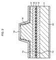
- Fig. 2 is a cross-sectional view showing the structure of the quantum dot optical amplifier 1. Fig. 2 only shows a part corresponding to the one input and the one output.
- an In 0.52 Al 0.24 Ga 0.24 As layer (InAlGaAs layer) 12 is formed on an n-type InP substrate 11.
- a surface of the n-type InP substrate 11 has a plane direction of (311) B.
- the InAlGaAs layer 12 has a thickness of, for example, 180 nm approximately.
- an InAs SK dot layer 13 is formed on the InAs SK dot layer 13.
- a plurality of projecting parts having a triangular pyramid shape are formed, which have a thickness of, for example, 1 to 3 nm approximately.
- an In 0.52 Al 0.24 Ga 0.24 As layer (InAlGaAs layer) 14 is formed on the InAs SK dot layer 13.
- the InAlGaAs layer 14 has a thickness of, for example, 30 nm approximately at the thickest part thereof.
- an InAs SK dot layer 15 is formed on the InAlGaAs layer 14.
- an In 0.52 Al 0.24 Ga 0.24 As layer (InAlGaAs layer) 16 is formed on the InAs SK dot layer 15.
- the InAlGaAs layer 16 has a thickness of, for example, 30 nm approximately at the thickest part thereof.
- a p-type InP layer 17 is formed, and a SiO 2 layer 18 having an opening is formed thereon.
- an electrode 19 connected to the p-type InP layer 17 via the opening is formed.
- an electrode 20 is formed on a reverse surface of the n-type InP substrate 11.
- the quantum dot optical amplifier 1 with such a configuration amplifies and outputs an optical signal introduced into an active layer when a voltage is applied between the electrodes 19 and 20.
- this quantum dot optical amplifier 1 has polarized wave dependency, and thus it cannot amplify a specific electric field component using only the single structure shown in Fig. 2. Accordingly, in this embodiment, the quantum dot optical amplifier 1 has two structures shown in Fig. 2.
- a polarization beam splitter (demultiplexer) 2 with one input and two outputs is provided.
- one optical fiber 10 is connected, and to the two output sections of the polarization beam splitter 2, optical fibers 10 respectively connected to the input sections of the quantum dot optical amplifier 1 are connected one by one.
- the polarization beam splitter 2 divides an inputted optical signal into two electric field components that are orthogonal to each other, and output them from the two output sections.
- the two optical fibers 10 connected to the output sections of the polarization beam splitter 2 are connected to the input sections of the quantum dot optical amplifier 1 in a state that both of the optical fibers have an electric field whose direction being adjusted to maximize its gain (amplification efficiency).
- the two electric field components outputted from the polarization beam splitter 2 are orthogonal to each other, so that one optical fiber 10 is twisted by 90° to the other optical fiber 10 between the polarization beam splitter 2 and the quantum dot optical amplifier 1.
- a polarization beam splitter (multiplexer) 3 with two inputs and one output is provided on the downstream side of the quantum dot optical amplifier 1.
- the polarization beam splitter 3 is provided to have the inputs and output in reverse to those of the polarization beam splitter 2.
- optical fibers 10 respectively connected to the output sections of the quantum dot optical amplifier 1 are connected one by one, and to the output section of the polarization beam splitter 3, one optical fiber 10 is connected.
- the polarization beam splitter 3 couples inputted optical signals of two electric field components that are orthogonal to each other and outputs the coupled signal. However, the electric fields of optical signals outputted from the two output sections of the quantum dot optical amplifier 1 have directions corresponding to each other.
- an optical signal outputted from the polarization beam splitter 3 is a signal in which all of the electric field components of the optical signal inputted to the polarization beam splitter 2 are amplified.
- a variable optical attenuator 4 and a gain equalizing filter 5 are provided on the downstream side of the polarization beam splitter 3, a variable optical attenuator 4 and a gain equalizing filter 5 are provided.
- the polarization beam splitter 3, the variable optical attenuator 4 and the gain equalizing filter 5 are connected to each other via the optical fiber 10.
- An optical signal outputted from the gain equalizing filter 5 is outputted as an output signal of the optical repeater.
- an optical detector 6 to which an inputted signal (optical signal) to the optical repeater is inputted, an optical detector 7 to which an optical signal outputted from the variable optical attenuator 4 is inputted, and an automatic gain control circuit 8 that performs control of the variable optical attenuator 4 based on output signals (electric signals) of the optical detectors 6 and 7 are provided.
- the variable optical attenuator 4 attenuates, based on the control performed by the automatic gain control circuit 8, an optical signal outputted from the polarization beam splitter 3 regardless of its wavelength, and outputs the attenuated signal.
- the gain equalizing filter 5 substantially uniformizes a gain of an optical signal outputted from the variable optical attenuator 4 within a predetermined range, and outputs the substantially uniformized signal.
- the automatic gain control circuit 8 controls, based on output signals of the optical detectors 6 and 7, degree of attenuation in the variable optical attenuator 4 so as to make a gain in the optical repeater to be a predetermined value.
- optical signal outputted from the polarization beam splitter 2 are amplified by the quantum dot optical amplifier 1 and coupled by the polarization beam splitter 3.
- a gain of the optical signal is then adjusted by the variable optical attenuator 4, and the gain is equalized between its wavelengths by the gain equalizing filter 5.
- the optical signal outputted from the variable optical attenuator 4 is also inputted to the optical detector 7, and its intensity is detected therein. This intensity is converted into an electric signal and outputted to the automatic gain control circuit 8.
- the gain adjustment by the variable optical attenuator 4 is controlled by the automatic gain control circuit 8.
- the polarized wave dependency found by the inventor of the present invention that is a drawback of previously-proposed optical repeaters is resolved.
- optical amplification of a wide wavelength range becomes possible.
- the number of active layers is not particularly limited, which may be one layer, three layers or more.
- FIG. 3 is a schematic view showing the structure of an optical repeater according to the second embodiment of the present invention.
- an optical detector 26 on a semiconductor substrate that is an InP substrate 33 for example, an optical detector 26, a TE/TM demultiplexer 22, a TE/TM converter 31, a phase controller 32, a multiplexer 23, a quantum dot optical amplifier 21, an intensity modulator (variable optical attenuator) 24, and an optical detector 27 are monolithically integrated.
- the TE/TM converter 31 and the phase controller 32 are arranged so as to respectively input a light of a TM mode and a light of a TE mode outputted from the TE/TM demultiplexer 22.
- the multiplexer 23 is arranged so as to couple lights outputted from the TE/TM converter 31 and the phase controller 32 to output the coupled light.
- an automatic gain/level control circuit 28 that performs control of the intensity modulator 24 based on intensities of lights detected by the optical detectors 26 and 27, and a gain equalizing filter (not-shown) are provided separately from the InP substrate 33.
- an input terminal and an output terminal of a waveguide 30 are slanted by about 10° from a vertical direction of end surfaces of the InP substrate 33. Also, on the end surfaces of the InP substrate 33, broadband antireflection coatings are applied.
- an intensity of the optical signal is detected by the optical detector 26, and this optical signal is thereafter divided by the TE/TM demultiplexer 22 into a TE wave and a TM wave.
- the intensity detected by the optical detector 26 is converted into an electric signal and outputted to the automatic gain/level control circuit 28.
- the TM wave is inputted to the TE/TM converter 31, converted into a TE wave and thereafter outputted.
- the TE wave outputted from the TE/TM demultiplexer 22 is controlled in its phase by the phase controller 32 in such a manner that the TE wave outputted from the TE/TM converter 31 and the TE wave outputted from the phase controller 32 intensify with each other in the multiplexer 23, and is thereafter outputted.
- the TE wave outputted from the TE/TM converter 31 and the TE wave outputted from the phase controller 32 are intensified with each other and coupled by the multiplexer 23, and outputted in a TE mode from the multiplexer 23.
- This outputted signal is amplified by the quantum dot optical amplifier 21.
- This outputted signal is then modulated in its intensity by the intensity modulator 24, thereafter inputted to the optical detector 27, and its intensity is detected therein. This intensity is converted into an electric signal and outputted to the automatic gain/level control circuit 28.
- the modulation of intensity by the intensity modulator 24 is controlled by the automatic gain/level control circuit 28.
- An optical signal outputted from the optical detector 27 is outputted from the InP substrate 33, and its gain is equalized between its wavelengths by a gain equalizing filter (not-shown) connected to the InP substrate 33 with, for example, an optical fiber.
- the polarized wave dependency found by the inventor of the present invention that is a drawback of previously-proposed optical repeaters is resolved.
- a result shown in Fig. 4 was obtained.
- a high light-emitting intensity was obtained for a broadband wavelength ranging from 1300 nm to 1600 nm.
- an effective light-emitting intensity is obtained, even with wider estimation, only in a range from 70 nm to 80 nm between 1500 nm to 1600 nm approximately.
- FIG. 5 is a schematic view showing the structure of an optical repeater according to the third embodiment of the present invention.
- an optical detector 26 on a semiconductor substrate that is an InP substrate 33 for example, an optical detector 26, a TE/TM demultiplexer 22, a TE/TM converter 31, quantum dot optical amplifiers 21a and 21b, a TE/TM converter 34, a TE/TM demultiplexer 35, an intensity modulator 24 and an optical detector 27 are monolithically integrated.
- the TE/TM converter 31 is arranged so as to input a light of a TM mode outputted from the TE/TM demultiplexer 22.
- the quantum dot optical amplifier 21a is arranged so as to input a TE wave outputted from the TE/TM converter 31, and the quantum dot optical amplifier 21b is arranged so as to input a TE wave outputted from the TE/TM demultiplexer 22.
- the TE/TM converter 34 is arranged in a reverse direction of the TE/TM converter 31, and a TE wave outputted from the quantum dot optical amplifier 21a is converted into a TM wave by the TE/TM converter 34.
- the TE/TM demultiplexer 35 is arranged in a reverse direction of the TE/TM demultiplexer 22, and a TE wave outputted from the quantum dot optical amplifier 21b and a TM wave outputted from the TE/TM converter 34 are coupled by the TE/TM demultiplexer 35.
- elements are integrated as a PLC (Planar Lightwave Circuit) on a quartz substrate.
- PLC Planar Lightwave Circuit
- waveguides are formed on the quartz substrate, and on this quartz substrate, among the components shown in Fig. 1, the quantum dot optical amplifier 1, the polarization beam splitters 2 and 3, the variable optical attenuator 4, and the light detectors 6 and 7 are integrated as the PLC.
- the optical detectors 26 and 27, the TE/TM demultiplexer 22, the TE/TM converter 31, the phase controller 32, the multiplexer 23, the quantum dot optical amplifier 21, and the intensity modulator 24 among the components of the second embodiment shown in Fig. 3 are integrated as the PLC on a quartz substrate, the similar effects can be obtained.
- the quantum dot optical amplifier is used as an optical amplifier, but a quantum wire optical amplifier, a quantum dash optical amplifier, or a quantum well optical amplifier may be used.
- an output power may be controlled based only on an intensity detected by the optical detector on the output side.
- the gain equalizing filter may be integrated as a semiconductor with the semiconductor optical amplifier.
- a broadband optical signal can be repeated, which is suitable for use in Coarse WDM communication for example.
Landscapes
- Physics & Mathematics (AREA)
- Engineering & Computer Science (AREA)
- Electromagnetism (AREA)
- Signal Processing (AREA)
- Computer Networks & Wireless Communication (AREA)
- Optics & Photonics (AREA)
- Nanotechnology (AREA)
- Chemical & Material Sciences (AREA)
- Biophysics (AREA)
- Crystallography & Structural Chemistry (AREA)
- Life Sciences & Earth Sciences (AREA)
- General Physics & Mathematics (AREA)
- Condensed Matter Physics & Semiconductors (AREA)
- Optical Communication System (AREA)
- Semiconductor Lasers (AREA)
Abstract
Description
- This application is based upon and claims the benefit of priority from the prior Japanese Patent Application No. 2002-338415, filed on November 21, 2002, the entire contents of which are incorporated herein by reference.
- The present invention relates to an optical repeater that is preferable as a 1R repeater of optical communication.
- For lowering the cost of metro-access optical communication networks, WDM (Wavelength Division Multiplexing) communication having a large wavelength interval between channels (Coarse WDM communication) is expected to be widely used in the coming years. The wavelength interval in the Coarse WDM communication is approximately equal to or less than 20 nm. In this system, it becomes possible to lower costs for such reasons that it is not necessary to precisely control wavelengths of a light source and a filter, and a cooler used for keeping the temperature of a semiconductor laser of a light source is unnecessary because a certain amount of wavelength variation is tolerated.
- In optical communication, an optical repeater is used for a purpose such as amplifying an attenuated optical signal. As the optical repeater, there exists a type in which a semiconductor optical amplifier and a gain equalizing filter are used. Regarding the semiconductor optical amplifiers, there exists a type in which a quantum well structure or a distorted quantum well structure is used for its active layer.
- In a metro communication network over a long distance, a 1R repeater is indispensable to compensate for loss in each node of the metro communication network.
- Prior arts are disclosed in Japanese Patent Laid-open No. 2000-40852 and in Japanese Patent Laid-open No. 2001-57455, for example.
- However, in the Coarse WDM communication, the wavelength range (band) to be used is so wide as to range from 1.3 µm to 1.6 µm, so that it is impossible to be amplified by a single previously-proposed optical amplifier (having a band of 0.05 µm approximately), which increases the cost of amplifying the whole wavelength range. Consequently, previously-proposed optical repeaters used in the Coarse WDM communication are also high-cost, so a cost reduction thereof has been desired.
- It is desirable to solve the above-described problems, and in particular to provide a low cost optical repeater suitable for use in Coarse WDM communication having a wide bandwidth.
- As a result of earnest studies, the inventor of the present invention has found that, in semiconductor optical amplifiers that include an active layer having a quantum well structure or the like, carrier density in the active layer improves at a critical current density by reducing the density of the active layer so that a gain spectrum can be broadband, but on the other hand, polarized wave dependency of the gain occurs due to asymmetry of the material of the active layer. Due to the occurrence of such polarized wave dependency, amplification of a wide wavelength range by previously-proposed optical amplifiers becomes difficult. Based on this viewpoint, the inventor of the present invention has devised the following aspects of the invention.
- According to a first aspect of the present invention an optical repeater has a semiconductor optical amplifier including an active layer that has one type of structure selected from a group composed of a quantum dot, a quantum wire, a quantum dash and a quantum well. Further, the optical repeater has a demultiplexer for dividing an inputted light into two components, and respective components of a light outputted from this demultiplexer are amplified by the semiconductor optical amplifier. Further, the optical repeater has a multiplexer for coupling two components of a light outputted from the semiconductor optical amplifier.
- In this optical repeater, the demultiplexer is provided on the upstream side of the semiconductor optical amplifier, and the multiplexer is provided on the downstream side. Consequently, the polarized wave dependency found by the inventor of the present invention that is a drawback of previously-proposed optical repeaters is resolved. As a result, optical amplification over a wide wavelength range becomes possible. In other words, the optical repeater according to this aspect of the present invention makes it possible to amplify the whole wavelength range using a single unit, which allows drastic cost reduction.
- According to a second aspect of the present invention an optical repeater has a semiconductor optical amplifier including an active layer that has one type of structure selected from a group composed of a quantum dot, a quantum wire, a quantum dash and a quantum well. Further, the optical repeater has a demultiplexer for dividing an inputted light into a TE wave and a TM wave, a converter for converting the TM wave into a TE wave, and a multiplexer for coupling the TE wave outputted from the demultiplexer and the TE wave outputted from the converter. The light outputted from the multiplexer is amplified by the semiconductor optical amplifier.
- In this optical repeater, the optical signal inputted to the semiconductor optical amplifier is only a TE wave, so that the polarized wave dependency found by the inventor of the present invention that is the drawback of previously-proposed optical repeaters is resolved.
- Reference will now be made by way of examples to the accompanying drawings, in which:
- Fig. 1 is a schematic view showing the structure of an optical repeater according to a first embodiment of the present invention;
- Fig. 2 is a cross-sectional view showing the structure of a quantum dot optical amplifier 1;
- Fig. 3 is a schematic view showing the structure of an optical repeater according to a second embodiment of the present invention;
- Fig. 4 is a graph showing an ASE (Amplitude Spontaneous Emission) spectrum that is actually obtained; and
- Fig. 5 is a schematic view showing the structure of an optical repeater according to a third embodiment of the present invention.
-
- First, a first embodiment of the present invention will be explained. Fig. 1 is a schematic view showing the structure of an optical repeater according to the first embodiment of the present invention.
- This embodiment has a quantum dot optical amplifier (semiconductor optical amplifier) 1 with two inputs and two outputs. The quantum dot optical amplifier 1 amplifies optical signals inputted to two input sections independently to each other. Specifically, the quantum dot optical amplifier 1 amplifies an optical signal inputted to one input section and outputs it thereafter from one output section, and amplifies an optical signal inputted to the other input section and outputs it thereafter from the other output section.
- Fig. 2 is a cross-sectional view showing the structure of the quantum dot optical amplifier 1. Fig. 2 only shows a part corresponding to the one input and the one output.
- In this quantum dot optical amplifier 1, an In0.52Al0.24Ga0.24As layer (InAlGaAs layer) 12 is formed on an n-type InP substrate 11. A surface of the n-type InP substrate 11 has a plane direction of (311) B. The InAlGaAs
layer 12 has a thickness of, for example, 180 nm approximately. Further, on the InAlGaAslayer 12, an InAs SKdot layer 13 is formed. On the InAs SKdot layer 13, a plurality of projecting parts having a triangular pyramid shape are formed, which have a thickness of, for example, 1 to 3 nm approximately. Further, on the InAsSK dot layer 13, an In0.52Al0.24Ga0.24As layer (InAlGaAs layer) 14 is formed. The InAlGaAslayer 14 has a thickness of, for example, 30 nm approximately at the thickest part thereof. On the InAlGaAslayer 14, an InAs SKdot layer 15 is formed. On the InAs SKdot layer 15, similarly to the InAsSK dot layer 13, a plurality of projecting parts having a triangular pyramid shape are formed, which have a thickness of, for example, 1 to 3 nm approximately. On the InAs SKdot layer 15, an In0.52Al0.24Ga0.24As layer (InAlGaAs layer) 16 is formed. The InAlGaAs layer 16 has a thickness of, for example, 30 nm approximately at the thickest part thereof. - Furthermore, on the InAlGaAs layer 16, a p-type InP layer 17 is formed, and a SiO2 layer 18 having an opening is formed thereon. On the SiO2 layer 18, an
electrode 19 connected to the p-type InP layer 17 via the opening is formed. Also, on a reverse surface of the n-type InP substrate 11, anelectrode 20 is formed. - The quantum dot optical amplifier 1 with such a configuration amplifies and outputs an optical signal introduced into an active layer when a voltage is applied between the
electrodes - On the upstream side of the quantum dot optical amplifier 1, a polarization beam splitter (demultiplexer) 2 with one input and two outputs is provided. To the input section of the
polarization beam splitter 2, oneoptical fiber 10 is connected, and to the two output sections of thepolarization beam splitter 2,optical fibers 10 respectively connected to the input sections of the quantum dot optical amplifier 1 are connected one by one. Thepolarization beam splitter 2 divides an inputted optical signal into two electric field components that are orthogonal to each other, and output them from the two output sections. The twooptical fibers 10 connected to the output sections of thepolarization beam splitter 2 are connected to the input sections of the quantum dot optical amplifier 1 in a state that both of the optical fibers have an electric field whose direction being adjusted to maximize its gain (amplification efficiency). Specifically, the two electric field components outputted from thepolarization beam splitter 2 are orthogonal to each other, so that oneoptical fiber 10 is twisted by 90° to the otheroptical fiber 10 between thepolarization beam splitter 2 and the quantum dot optical amplifier 1. - On the downstream side of the quantum dot optical amplifier 1, a polarization beam splitter (multiplexer) 3 with two inputs and one output is provided. The
polarization beam splitter 3 is provided to have the inputs and output in reverse to those of thepolarization beam splitter 2. To the two input sections of thepolarization beam splitter 3,optical fibers 10 respectively connected to the output sections of the quantum dot optical amplifier 1 are connected one by one, and to the output section of thepolarization beam splitter 3, oneoptical fiber 10 is connected. Thepolarization beam splitter 3 couples inputted optical signals of two electric field components that are orthogonal to each other and outputs the coupled signal. However, the electric fields of optical signals outputted from the two output sections of the quantum dot optical amplifier 1 have directions corresponding to each other. Accordingly, in order to make these electric field components orthogonal to each other similarly to the optical signal inputted to thepolarization beam splitter 2, the oneoptical fiber 10 is twisted by 90° to the otheroptical fiber 10. This twisting direction is reverse to the twisting direction of the twooptical fibers 10 connected to the input sections of the quantum dot optical amplifier 1. Therefore, an optical signal outputted from thepolarization beam splitter 3 is a signal in which all of the electric field components of the optical signal inputted to thepolarization beam splitter 2 are amplified. - On the downstream side of the
polarization beam splitter 3, a variableoptical attenuator 4 and a gain equalizing filter 5 are provided. Thepolarization beam splitter 3, the variableoptical attenuator 4 and the gain equalizing filter 5 are connected to each other via theoptical fiber 10. An optical signal outputted from the gain equalizing filter 5 is outputted as an output signal of the optical repeater. Further, an optical detector 6 to which an inputted signal (optical signal) to the optical repeater is inputted, an optical detector 7 to which an optical signal outputted from the variableoptical attenuator 4 is inputted, and an automaticgain control circuit 8 that performs control of the variableoptical attenuator 4 based on output signals (electric signals) of the optical detectors 6 and 7 are provided. - The variable
optical attenuator 4 attenuates, based on the control performed by the automaticgain control circuit 8, an optical signal outputted from thepolarization beam splitter 3 regardless of its wavelength, and outputs the attenuated signal. The gain equalizing filter 5 substantially uniformizes a gain of an optical signal outputted from the variableoptical attenuator 4 within a predetermined range, and outputs the substantially uniformized signal. The automaticgain control circuit 8 controls, based on output signals of the optical detectors 6 and 7, degree of attenuation in the variableoptical attenuator 4 so as to make a gain in the optical repeater to be a predetermined value. - When an optical signal is inputted to the optical repeater according to this embodiment with the above-described configuration, this optical signal is divided by the
polarization beam splitter 2, and its intensity is detected by the optical detector 6. This intensity is converted into an electric signal and outputted to the automaticgain control circuit 8. Thereafter, optical signals outputted from thepolarization beam splitter 2 are amplified by the quantum dot optical amplifier 1 and coupled by thepolarization beam splitter 3. A gain of the optical signal is then adjusted by the variableoptical attenuator 4, and the gain is equalized between its wavelengths by the gain equalizing filter 5. The optical signal outputted from the variableoptical attenuator 4 is also inputted to the optical detector 7, and its intensity is detected therein. This intensity is converted into an electric signal and outputted to the automaticgain control circuit 8. Incidentally, the gain adjustment by the variableoptical attenuator 4 is controlled by the automaticgain control circuit 8. - According to this embodiment, with the
polarization beam splitters - Incidentally, in the structure shown in Fig. 2, two layers that are the InAs SK dot layers 13 and 15 are formed as the active layer. However, the number of active layers is not particularly limited, which may be one layer, three layers or more.
- Next, a second embodiment of the present invention will be explained. In this embodiment, elements are monolithically integrated on a semiconductor substrate. Fig. 3 is a schematic view showing the structure of an optical repeater according to the second embodiment of the present invention.
- In this embodiment, on a semiconductor substrate that is an
InP substrate 33 for example, anoptical detector 26, a TE/TM demultiplexer 22, a TE/TM converter 31, aphase controller 32, amultiplexer 23, a quantum dotoptical amplifier 21, an intensity modulator (variable optical attenuator) 24, and anoptical detector 27 are monolithically integrated. The TE/TM converter 31 and thephase controller 32 are arranged so as to respectively input a light of a TM mode and a light of a TE mode outputted from the TE/TM demultiplexer 22. Themultiplexer 23 is arranged so as to couple lights outputted from the TE/TM converter 31 and thephase controller 32 to output the coupled light. - Further, an automatic gain/
level control circuit 28 that performs control of theintensity modulator 24 based on intensities of lights detected by theoptical detectors InP substrate 33. - Incidentally, an input terminal and an output terminal of a
waveguide 30 are slanted by about 10° from a vertical direction of end surfaces of theInP substrate 33. Also, on the end surfaces of theInP substrate 33, broadband antireflection coatings are applied. - When an optical signal is inputted to the optical repeater according to the second embodiment with the above-described configuration, an intensity of the optical signal is detected by the
optical detector 26, and this optical signal is thereafter divided by the TE/TM demultiplexer 22 into a TE wave and a TM wave. The intensity detected by theoptical detector 26 is converted into an electric signal and outputted to the automatic gain/level control circuit 28. The TM wave is inputted to the TE/TM converter 31, converted into a TE wave and thereafter outputted. On the other hand, the TE wave outputted from the TE/TM demultiplexer 22 is controlled in its phase by thephase controller 32 in such a manner that the TE wave outputted from the TE/TM converter 31 and the TE wave outputted from thephase controller 32 intensify with each other in themultiplexer 23, and is thereafter outputted. - Thereafter, the TE wave outputted from the TE/
TM converter 31 and the TE wave outputted from thephase controller 32 are intensified with each other and coupled by themultiplexer 23, and outputted in a TE mode from themultiplexer 23. This outputted signal is amplified by the quantum dotoptical amplifier 21.
This outputted signal is then modulated in its intensity by theintensity modulator 24, thereafter inputted to theoptical detector 27, and its intensity is detected therein. This intensity is converted into an electric signal and outputted to the automatic gain/level control circuit 28. The modulation of intensity by theintensity modulator 24 is controlled by the automatic gain/level control circuit 28. An optical signal outputted from theoptical detector 27 is outputted from theInP substrate 33, and its gain is equalized between its wavelengths by a gain equalizing filter (not-shown) connected to theInP substrate 33 with, for example, an optical fiber. - According to this embodiment, with the TE/
TM demultiplexer 22 and themultiplexer 23, the polarized wave dependency found by the inventor of the present invention that is a drawback of previously-proposed optical repeaters is resolved. As a result, similarly to the first embodiment, it becomes possible to amplify an optical signal having a wide wavelength range, which allows drastic cost reduction. - When the inventor of the present invention actually fabricated the optical repeater (the second embodiment) shown in Fig. 3 and measured its gain spectrum, a result shown in Fig. 4 was obtained. As shown in Fig. 4, a high light-emitting intensity was obtained for a broadband wavelength ranging from 1300 nm to 1600 nm. With the previously-proposed optical repeater, an effective light-emitting intensity is obtained, even with wider estimation, only in a range from 70 nm to 80 nm between 1500 nm to 1600 nm approximately.
- In addition, in this fabricated optical repeater, dependency of its gain on a polarized wave was quite low, and the gain was approximately uniform over a broadband wavelength. Further, automatic control of the gain was also possible.
- Next, a third embodiment of the present invention will be explained. Also in the third embodiment, similarly to the second embodiment, elements are monolithically integrated on a semiconductor substrate. Fig. 5 is a schematic view showing the structure of an optical repeater according to the third embodiment of the present invention.
- In this embodiment, on a semiconductor substrate that is an
InP substrate 33 for example, anoptical detector 26, a TE/TM demultiplexer 22, a TE/TM converter 31, quantum dotoptical amplifiers TM converter 34, a TE/TM demultiplexer 35, anintensity modulator 24 and anoptical detector 27 are monolithically integrated. - The TE/
TM converter 31 is arranged so as to input a light of a TM mode outputted from the TE/TM demultiplexer 22. The quantum dotoptical amplifier 21a is arranged so as to input a TE wave outputted from the TE/TM converter 31, and the quantum dotoptical amplifier 21b is arranged so as to input a TE wave outputted from the TE/TM demultiplexer 22. The TE/TM converter 34 is arranged in a reverse direction of the TE/TM converter 31, and a TE wave outputted from the quantum dotoptical amplifier 21a is converted into a TM wave by the TE/TM converter 34. Further, the TE/TM demultiplexer 35 is arranged in a reverse direction of the TE/TM demultiplexer 22, and a TE wave outputted from the quantum dotoptical amplifier 21b and a TM wave outputted from the TE/TM converter 34 are coupled by the TE/TM demultiplexer 35. - By the third embodiment configured as above, the similar effects as those of the second embodiment can be obtained.
- Next, a fourth embodiment of the present invention will be explained. In the fourth embodiment, elements are integrated as a PLC (Planar Lightwave Circuit) on a quartz substrate. Specifically, waveguides are formed on the quartz substrate, and on this quartz substrate, among the components shown in Fig. 1, the quantum dot optical amplifier 1, the
polarization beam splitters optical attenuator 4, and the light detectors 6 and 7 are integrated as the PLC. - By the fourth embodiment configured as above, the similar effects as those of the first embodiment can be obtained.
- When the
optical detectors TM demultiplexer 22, the TE/TM converter 31, thephase controller 32, themultiplexer 23, the quantum dotoptical amplifier 21, and theintensity modulator 24 among the components of the second embodiment shown in Fig. 3 are integrated as the PLC on a quartz substrate, the similar effects can be obtained. - Incidentally, in the first to fourth embodiments, the quantum dot optical amplifier is used as an optical amplifier, but a quantum wire optical amplifier, a quantum dash optical amplifier, or a quantum well optical amplifier may be used.
- Further, for controlling the variable optical attenuator and the intensity modulator, an output power may be controlled based only on an intensity detected by the optical detector on the output side.
- Further, the gain equalizing filter may be integrated as a semiconductor with the semiconductor optical amplifier.
- As described in detail above, according to the present invention, a broadband optical signal can be repeated, which is suitable for use in Coarse WDM communication for example.
- The present embodiments are to be considered in all respects as illustrative and not restrictive, and all changes which come within the meaning and range of equivalency of the claims are therefore intended to be embraced therein. The invention may be embodied in other specific forms without departing from the spirit or essential characteristics thereof.
Claims (19)
- An optical repeater, comprising:a demultiplexer for dividing an inputted light into two components;a semiconductor optical amplifier including an active layer that has one type of structure selected from a group composed of a quantum dot, a quantum wire, a quantum dash, and a quantum well, and amplifying respective components of a light outputted from said demultiplexer; anda multiplexer for coupling two components of a light outputted from said semiconductor optical amplifier.
- The optical repeater according to claim 1, wherein said demultiplexer is a polarization beam splitter for dividing the inputted light into two components that are orthogonal to each other.
- The optical repeater according to claim 1 or 2, wherein said demultiplexer divides the inputted light into a TE wave and a TM wave.
- The optical repeater according to any preceding claim, wherein said demultiplexer and said multiplexer are monolithically integrated with said semiconductor optical amplifier.
- The optical repeater according to claims 1 to 3, wherein said demultiplexer and said multiplexer are integrated as a Planar Lightwave Circuit with said semiconductor optical amplifier.
- The optical repeater according to any preceding claim, further comprising:a variable optical attenuator for attenuating a light outputted from said multiplexer;an output detector for detecting an intensity of a light outputted from said variable optical attenuator; andan output controller for controlling an intensity of an output signal by controlling operation of said variable optical attenuator based on the intensity detected by said output detector.
- An optical repeater, comprising:a demultiplexer for dividing an inputted light into a TE wave and a TM wave;a converter for converting the TM wave into a TE wave;a multiplexer for coupling a TE wave outputted from said demultiplexer and a TE wave outputted from said converter; anda semiconductor optical amplifier including an active layer that has one type of structure selected from a group composed of a quantum dot, a quantum wire, a quantum dash, and a quantum well, and amplifying a light outputted from said multiplexer.
- The optical repeater according to claim 7, further comprising a phase controller for controlling a phase of the TE wave outputted from said demultiplexer so that the TE wave intensifies with a TE wave outputted from said converter in said multiplexer.
- The optical repeater according to claim 7 or 8, wherein said demultiplexer, said converter and said multiplexer are monolithically integrated with said semiconductor optical amplifier.
- The optical repeater according to claim 7 or 8, wherein said demultiplexer, said converter and said multiplexer are integrated as a Planar Lightwave Circuit with said semiconductor optical amplifier.
- The optical repeater according to any one of claims 7 to 10, further comprising:a variable optical attenuator for attenuating a light outputted from said semiconductor optical amplifier;an output detector for detecting an intensity of a light outputted from said variable optical attenuator; andan output controller for controlling an intensity of an output signal by controlling operation of said variable optical attenuator based on the intensity detected by said output detector.
- The optical repeater according to claim 6 or 11, wherein said variable optical attenuator and said output detector are monolithically integrated with said semiconductor optical amplifier.
- The optical repeater according to claim 6 or 11, wherein said variable optical attenuator and said output detector are integrated as a Planar Lightwave Circuit with said semiconductor optical amplifier.
- The optical repeater according to any preceding claim, further comprising:an input detector for detecting an intensity of the inputted light;a variable optical attenuator for attenuating a light outputted from said multiplexer;an output detector for detecting an intensity of a light outputted from said variable optical attenuator; anda gain controller for controlling a gain by controlling operation of said variable optical attenuator based on the intensity detected by said input detector and the intensity detected by said output detector.
- The optical repeater according to claim 14, wherein said input detector, said variable optical attenuator and said output detector are monolithically integrated with said semiconductor optical amplifier.
- The optical repeater according to claim 14, wherein said input detector, said variable optical attenuator and said output detector are integrated as a Planar Lightwave Circuit with said semiconductor optical amplifier.
- The optical repeater according to any preceding claim, further comprising a gain equalizer for controlling a gain of a light outputted from said semiconductor optical amplifier within a range within a predetermined wavelength band.
- The optical repeater according to claim 17 wherein said gain equalizer is integrated on a semiconductor substrate with said semiconductor optical amplifier.
- The optical repeater according to any preceding claim wherein said optical repeater is used as a 1R repeater.
Applications Claiming Priority (2)
| Application Number | Priority Date | Filing Date | Title |
|---|---|---|---|
| JP2002338415 | 2002-11-21 | ||
| JP2002338415A JP4359035B2 (en) | 2002-11-21 | 2002-11-21 | Optical repeater |
Publications (2)
| Publication Number | Publication Date |
|---|---|
| EP1422844A1 true EP1422844A1 (en) | 2004-05-26 |
| EP1422844B1 EP1422844B1 (en) | 2006-09-20 |
Family
ID=32212128
Family Applications (1)
| Application Number | Title | Priority Date | Filing Date |
|---|---|---|---|
| EP03257286A Expired - Lifetime EP1422844B1 (en) | 2002-11-21 | 2003-11-19 | Optical repeater |
Country Status (4)
| Country | Link |
|---|---|
| US (2) | US7375878B2 (en) |
| EP (1) | EP1422844B1 (en) |
| JP (1) | JP4359035B2 (en) |
| DE (1) | DE60308464T2 (en) |
Cited By (1)
| Publication number | Priority date | Publication date | Assignee | Title |
|---|---|---|---|---|
| EP2670072A4 (en) * | 2011-01-24 | 2016-04-06 | Nec Corp | POLARIZED WAVE MULTIPLEXING OPTICAL RECEIVING DEVICE AND POLARIZED WAVE MULTIPLEXING OPTICAL RECEIVING METHOD |
Families Citing this family (25)
| Publication number | Priority date | Publication date | Assignee | Title |
|---|---|---|---|---|
| US8471852B1 (en) | 2003-05-30 | 2013-06-25 | Nvidia Corporation | Method and system for tessellation of subdivision surfaces |
| US20060189276A1 (en) * | 2004-12-08 | 2006-08-24 | Michael Halinski | Methods and systems for intelligent adaptive gain control |
| US8571346B2 (en) | 2005-10-26 | 2013-10-29 | Nvidia Corporation | Methods and devices for defective pixel detection |
| US7750956B2 (en) * | 2005-11-09 | 2010-07-06 | Nvidia Corporation | Using a graphics processing unit to correct video and audio data |
| US8588542B1 (en) | 2005-12-13 | 2013-11-19 | Nvidia Corporation | Configurable and compact pixel processing apparatus |
| US8737832B1 (en) | 2006-02-10 | 2014-05-27 | Nvidia Corporation | Flicker band automated detection system and method |
| US8594441B1 (en) | 2006-09-12 | 2013-11-26 | Nvidia Corporation | Compressing image-based data using luminance |
| US8723969B2 (en) * | 2007-03-20 | 2014-05-13 | Nvidia Corporation | Compensating for undesirable camera shakes during video capture |
| US8724895B2 (en) | 2007-07-23 | 2014-05-13 | Nvidia Corporation | Techniques for reducing color artifacts in digital images |
| US8570634B2 (en) * | 2007-10-11 | 2013-10-29 | Nvidia Corporation | Image processing of an incoming light field using a spatial light modulator |
| US9177368B2 (en) | 2007-12-17 | 2015-11-03 | Nvidia Corporation | Image distortion correction |
| US8780128B2 (en) | 2007-12-17 | 2014-07-15 | Nvidia Corporation | Contiguously packed data |
| US8698908B2 (en) | 2008-02-11 | 2014-04-15 | Nvidia Corporation | Efficient method for reducing noise and blur in a composite still image from a rolling shutter camera |
| US9379156B2 (en) * | 2008-04-10 | 2016-06-28 | Nvidia Corporation | Per-channel image intensity correction |
| US8373718B2 (en) | 2008-12-10 | 2013-02-12 | Nvidia Corporation | Method and system for color enhancement with color volume adjustment and variable shift along luminance axis |
| US8749662B2 (en) | 2009-04-16 | 2014-06-10 | Nvidia Corporation | System and method for lens shading image correction |
| US8698918B2 (en) | 2009-10-27 | 2014-04-15 | Nvidia Corporation | Automatic white balancing for photography |
| US8995049B2 (en) * | 2011-09-08 | 2015-03-31 | Northrop Grumman Systems Corporation | Method and apparatus for suppression of stimulated brillouin scattering using polarization control with a birefringent delay element |
| US9025241B2 (en) * | 2011-10-14 | 2015-05-05 | Kotura, Inc. | Gain medium providing laser and amplifier functionality to optical device |
| JP2013168500A (en) * | 2012-02-15 | 2013-08-29 | Mitsubishi Electric Corp | Optical semiconductor device |
| US9798698B2 (en) | 2012-08-13 | 2017-10-24 | Nvidia Corporation | System and method for multi-color dilu preconditioner |
| US9508318B2 (en) | 2012-09-13 | 2016-11-29 | Nvidia Corporation | Dynamic color profile management for electronic devices |
| US9307213B2 (en) | 2012-11-05 | 2016-04-05 | Nvidia Corporation | Robust selection and weighting for gray patch automatic white balancing |
| US9826208B2 (en) | 2013-06-26 | 2017-11-21 | Nvidia Corporation | Method and system for generating weights for use in white balancing an image |
| US9756222B2 (en) | 2013-06-26 | 2017-09-05 | Nvidia Corporation | Method and system for performing white balancing operations on captured images |
Citations (4)
| Publication number | Priority date | Publication date | Assignee | Title |
|---|---|---|---|---|
| EP0305995A2 (en) * | 1987-09-01 | 1989-03-08 | Nec Corporation | An optical amplifying repeater |
| US4923291A (en) * | 1987-07-23 | 1990-05-08 | Kokusai Denshin Denwa Kabushiki Kaisha | Optical amplification |
| EP0615323A2 (en) * | 1993-03-09 | 1994-09-14 | Canon Kabushiki Kaisha | A semiconductor optical amplifier which functions independently of polarization and an optical communication system using the same |
| US6421169B1 (en) * | 1997-02-14 | 2002-07-16 | Telefonaktiebolaget Lm Ericsson | Optical fiber amplifier having variable gain |
Family Cites Families (43)
| Publication number | Priority date | Publication date | Assignee | Title |
|---|---|---|---|---|
| DE3671986D1 (en) * | 1985-03-18 | 1990-07-19 | Nec Corp | DEVICE FOR REGULATING THE POLARIZATION WITH A BEAM SPLITTER. |
| US4900917A (en) * | 1988-07-15 | 1990-02-13 | American Telephone And Telegraph Company, At&T Bell Laboratories | Polarization insensitive optical communication device utilizing optical preamplification |
| US4941738A (en) * | 1988-07-29 | 1990-07-17 | American Telephone And Telegraph Company | Polarization independent optical amplifier apparatus |
| US4952017A (en) * | 1989-03-14 | 1990-08-28 | At&T Bell Laboratories | Polarization independent semiconductor optical amplifier |
| DE69104573T2 (en) * | 1990-08-03 | 1995-04-20 | Philips Nv | Optical amplifier. |
| NL9101244A (en) * | 1991-07-15 | 1993-02-01 | Nederland Ptt | POLARIZATION-SENSITIVE GAINING DEVICE. |
| SE509264C2 (en) * | 1992-01-30 | 1998-12-21 | Ericsson Telefon Ab L M | Apparatus and method for polarization-independent processing of an optical signal in a waveguide |
| JP2536288B2 (en) * | 1992-11-27 | 1996-09-18 | 日本電気株式会社 | Optical amplifier |
| US5303314A (en) * | 1993-03-15 | 1994-04-12 | The United States Of America As Represented By The Secretary Of The Navy | Method and apparatus for polarization-maintaining fiber optical amplification with orthogonal polarization output |
| JPH06347724A (en) | 1993-06-11 | 1994-12-22 | Canon Inc | Polarization independent optical element |
| BE1007282A3 (en) * | 1993-07-12 | 1995-05-09 | Philips Electronics Nv | An opto-electronic semiconductor device with an array of semiconductor diode lasers and a method for the production thereof. |
| EP0668641B1 (en) * | 1994-02-18 | 2001-06-06 | Canon Kabushiki Kaisha | Oscillation polarization mode selective semiconductor laser, light transmitter and optical communication system using the laser |
| US5659560A (en) * | 1994-05-12 | 1997-08-19 | Canon Kabushiki Kaisha | Apparatus and method for driving oscillation polarization selective light source, and optical communication system using the same |
| JP3204485B2 (en) * | 1995-03-31 | 2001-09-04 | キヤノン株式会社 | Optical semiconductor device and manufacturing method thereof |
| DE19612604A1 (en) * | 1996-03-29 | 1997-10-02 | Sel Alcatel Ag | Optical receiver with an equalizer circuit for interference caused by PMD and system with such an optical receiver |
| JPH09321701A (en) * | 1996-05-31 | 1997-12-12 | Fujitsu Ltd | Optical communication system and optical amplifier |
| US5822100A (en) * | 1996-06-26 | 1998-10-13 | Mci Communications Corporation | Method and system for equalizing PMD using incremental delay switching |
| JP2937148B2 (en) * | 1996-11-06 | 1999-08-23 | 日本電気株式会社 | Semiconductor integrated polarization mode converter |
| WO1998020376A1 (en) * | 1996-11-07 | 1998-05-14 | California Institute Of Technology | All-optical wavelength coded logic gates |
| JP4104718B2 (en) * | 1997-04-11 | 2008-06-18 | 富士ゼロックス株式会社 | Optical recording method |
| JP3952227B2 (en) * | 1997-10-20 | 2007-08-01 | 富士通株式会社 | Wavelength converter |
| JPH11243256A (en) * | 1997-12-03 | 1999-09-07 | Canon Inc | Distributed feedback semiconductor laser and its driving method. |
| JP3607497B2 (en) * | 1998-03-17 | 2005-01-05 | 日本電気株式会社 | Optical equalizer with gain equalizer and gain equalization function |
| JP3777045B2 (en) * | 1998-03-19 | 2006-05-24 | 富士通株式会社 | Polarization scrambler |
| JP3737628B2 (en) * | 1998-03-20 | 2006-01-18 | 富士通株式会社 | Gain equalizer and optical amplifier |
| JP2000011417A (en) * | 1998-06-26 | 2000-01-14 | Toshiba Corp | Semiconductor laser array and manufacturing method thereof, optical integrated unit, optical pickup, and optical disk drive |
| US6175446B1 (en) * | 1998-09-23 | 2001-01-16 | Sarnoff Corporation | Polarization-independent semiconductor optical amplifier |
| JP3802691B2 (en) | 1998-10-08 | 2006-07-26 | 日立電線株式会社 | Low noise semiconductor optical amplifier |
| JP3907861B2 (en) * | 1999-02-17 | 2007-04-18 | 富士通株式会社 | Method and apparatus for wavelength conversion and system including the apparatus |
| JP2001053392A (en) * | 1999-06-03 | 2001-02-23 | Fujitsu Ltd | Polarization independent semiconductor optical amplifier |
| US6384966B1 (en) * | 1999-11-03 | 2002-05-07 | Time-Bandwidth Products Ag | Multiple pass optical amplifier with thermal birefringence compensation |
| KR100353419B1 (en) * | 2000-03-10 | 2002-09-18 | 삼성전자 주식회사 | Polarization insensitive semiconductor optical amplifier |
| US20020054404A1 (en) * | 2000-03-17 | 2002-05-09 | Hedekvist Per Olof | Optical logic gates based on the polarization properties of four-wave mixing |
| US6928223B2 (en) * | 2000-07-14 | 2005-08-09 | Massachusetts Institute Of Technology | Stab-coupled optical waveguide laser and amplifier |
| CN1343906A (en) * | 2000-09-11 | 2002-04-10 | 三井化学株式会社 | Wavelength converter |
| JP4789320B2 (en) * | 2000-12-01 | 2011-10-12 | 富士通株式会社 | Semiconductor optical amplifier |
| JP4502500B2 (en) * | 2000-12-06 | 2010-07-14 | 富士通株式会社 | Optical time division multiplexed signal processing apparatus and processing method, and optical time division multiplexed signal receiving apparatus |
| EP1231488B1 (en) * | 2001-02-09 | 2010-03-31 | Panasonic Corporation | Optical device |
| US20020154387A1 (en) * | 2001-04-20 | 2002-10-24 | Kenji Mori | Gain equalizer, collimator with gain equalizer and method of manufacturing gain equalizer |
| JP4139577B2 (en) * | 2001-05-11 | 2008-08-27 | 富士通株式会社 | Optical signal processing method and optical signal processing apparatus |
| JP3950028B2 (en) * | 2001-10-05 | 2007-07-25 | 日本電信電話株式会社 | Optical amplifier |
| US7081983B2 (en) * | 2002-09-19 | 2006-07-25 | Fujitsu Limited | Wavelength conversion device |
| US7002733B2 (en) * | 2003-01-30 | 2006-02-21 | Quantum Photonics, Inc. | Methods and devices for amplifying optical signals using a depolarizer |
-
2002
- 2002-11-21 JP JP2002338415A patent/JP4359035B2/en not_active Expired - Fee Related
-
2003
- 2003-11-19 EP EP03257286A patent/EP1422844B1/en not_active Expired - Lifetime
- 2003-11-19 DE DE60308464T patent/DE60308464T2/en not_active Expired - Lifetime
- 2003-11-20 US US10/716,662 patent/US7375878B2/en not_active Expired - Lifetime
-
2008
- 2008-03-18 US US12/076,381 patent/US7616377B2/en not_active Expired - Fee Related
Patent Citations (4)
| Publication number | Priority date | Publication date | Assignee | Title |
|---|---|---|---|---|
| US4923291A (en) * | 1987-07-23 | 1990-05-08 | Kokusai Denshin Denwa Kabushiki Kaisha | Optical amplification |
| EP0305995A2 (en) * | 1987-09-01 | 1989-03-08 | Nec Corporation | An optical amplifying repeater |
| EP0615323A2 (en) * | 1993-03-09 | 1994-09-14 | Canon Kabushiki Kaisha | A semiconductor optical amplifier which functions independently of polarization and an optical communication system using the same |
| US6421169B1 (en) * | 1997-02-14 | 2002-07-16 | Telefonaktiebolaget Lm Ericsson | Optical fiber amplifier having variable gain |
Non-Patent Citations (1)
| Title |
|---|
| HOLTMANN C ET AL: "Monolithically Integrated Gain-clamped Semiconductor Optical Amplifier Exploiting Mach-zehnder Interferometer Configuration", ECOC'96, vol. 3, 15 September 1996 (1996-09-15), Oslo, pages 199 - 202, XP010303103 * |
Cited By (1)
| Publication number | Priority date | Publication date | Assignee | Title |
|---|---|---|---|---|
| EP2670072A4 (en) * | 2011-01-24 | 2016-04-06 | Nec Corp | POLARIZED WAVE MULTIPLEXING OPTICAL RECEIVING DEVICE AND POLARIZED WAVE MULTIPLEXING OPTICAL RECEIVING METHOD |
Also Published As
| Publication number | Publication date |
|---|---|
| EP1422844B1 (en) | 2006-09-20 |
| DE60308464D1 (en) | 2006-11-02 |
| US20040101313A1 (en) | 2004-05-27 |
| DE60308464T2 (en) | 2007-02-15 |
| JP4359035B2 (en) | 2009-11-04 |
| US7375878B2 (en) | 2008-05-20 |
| US20080240731A1 (en) | 2008-10-02 |
| US7616377B2 (en) | 2009-11-10 |
| JP2004172486A (en) | 2004-06-17 |
Similar Documents
| Publication | Publication Date | Title |
|---|---|---|
| US7616377B2 (en) | Optical repeater | |
| US7526150B2 (en) | Deployment of electro-optic amplitude varying elements (AVES) and electro-optic multi-functional elements (MFES) in photonic integrated circuits (PICS) | |
| US5576881A (en) | Multi-frequency optical signal source having reduced distortion and crosstalk | |
| US6731424B1 (en) | Dynamic gain flattening in an optical communication system | |
| JP2004524578A (en) | Wavelength converter with integrated absorber | |
| US20040099858A1 (en) | Semiconductor quantum dot optical amplifier, and optical amplifier module and optical transmission system using the same | |
| JP2024513714A (en) | Optical modulation amplifier, optical module, optical network unit and optical communication system | |
| EP0830721B1 (en) | Optical amplifier | |
| US12057888B2 (en) | Laser light system with wavelength attenuation | |
| Morito et al. | Record high saturation power (+ 22 dBm) and low noise figure (5.7 dB) polarization-insensitive SOA module | |
| Bernasconi et al. | Monolithically integrated 40-Gb/s switchable wavelength converter | |
| Doerr et al. | Elimination of signal distortion and crosstalk from carrier density changes in the shared semiconductor amplifier of multifrequency signal sources | |
| US6602002B1 (en) | High capacity optical transmission arrangement | |
| US7020168B2 (en) | High power multi-frequency laser | |
| Doerr et al. | Polarization diversity waveguide grating receiver with integrated optical preamplifiers | |
| Debrégeas et al. | Extremely high-power laser-modulators with integrated amplifier section (EML-SOAs) | |
| JP2002116419A (en) | Light modulation device and method of manufacturing the same | |
| EP1130826B1 (en) | Broad band optical amplifier using free space demultiplexing | |
| Bernasconi et al. | Monolithically integrated 40Gb/s wavelength converter with multi-frequency laser | |
| KR100420796B1 (en) | Semiconductor quantum dot optical amplification modules and optical transmission systems employing those modules | |
| JP4653940B2 (en) | Light controller for communication | |
| Banerjee et al. | Cascaded semiconductor optical amplifiers for transmission of 32 DWDM channels over 315 km | |
| US20030179441A1 (en) | Polarisation insensitive optical amplifiers | |
| Nicholes et al. | Large-scale photonic integration for advanced all-optical routing functions | |
| Loh et al. | Noise figure of a packaged, high-power slab-coupled optical waveguide amplifier (SCOWA) |
Legal Events
| Date | Code | Title | Description |
|---|---|---|---|
| PUAI | Public reference made under article 153(3) epc to a published international application that has entered the european phase |
Free format text: ORIGINAL CODE: 0009012 |
|
| AK | Designated contracting states |
Kind code of ref document: A1 Designated state(s): AT BE BG CH CY CZ DE DK EE ES FI FR GB GR HU IE IT LI LU MC NL PT RO SE SI SK TR |
|
| AX | Request for extension of the european patent |
Extension state: AL LT LV MK |
|
| 17P | Request for examination filed |
Effective date: 20041117 |
|
| AKX | Designation fees paid |
Designated state(s): DE FR GB |
|
| 17Q | First examination report despatched |
Effective date: 20050616 |
|
| GRAP | Despatch of communication of intention to grant a patent |
Free format text: ORIGINAL CODE: EPIDOSNIGR1 |
|
| GRAS | Grant fee paid |
Free format text: ORIGINAL CODE: EPIDOSNIGR3 |
|
| GRAA | (expected) grant |
Free format text: ORIGINAL CODE: 0009210 |
|
| AK | Designated contracting states |
Kind code of ref document: B1 Designated state(s): DE FR GB |
|
| REG | Reference to a national code |
Ref country code: GB Ref legal event code: FG4D |
|
| REF | Corresponds to: |
Ref document number: 60308464 Country of ref document: DE Date of ref document: 20061102 Kind code of ref document: P |
|
| ET | Fr: translation filed | ||
| PLBE | No opposition filed within time limit |
Free format text: ORIGINAL CODE: 0009261 |
|
| STAA | Information on the status of an ep patent application or granted ep patent |
Free format text: STATUS: NO OPPOSITION FILED WITHIN TIME LIMIT |
|
| 26N | No opposition filed |
Effective date: 20070621 |
|
| REG | Reference to a national code |
Ref country code: FR Ref legal event code: PLFP Year of fee payment: 13 |
|
| REG | Reference to a national code |
Ref country code: FR Ref legal event code: PLFP Year of fee payment: 14 |
|
| REG | Reference to a national code |
Ref country code: FR Ref legal event code: PLFP Year of fee payment: 15 |
|
| REG | Reference to a national code |
Ref country code: FR Ref legal event code: PLFP Year of fee payment: 16 |
|
| PGFP | Annual fee paid to national office [announced via postgrant information from national office to epo] |
Ref country code: FR Payment date: 20201013 Year of fee payment: 18 Ref country code: GB Payment date: 20201112 Year of fee payment: 18 Ref country code: DE Payment date: 20201103 Year of fee payment: 18 |
|
| REG | Reference to a national code |
Ref country code: DE Ref legal event code: R119 Ref document number: 60308464 Country of ref document: DE |
|
| GBPC | Gb: european patent ceased through non-payment of renewal fee |
Effective date: 20211119 |
|
| PG25 | Lapsed in a contracting state [announced via postgrant information from national office to epo] |
Ref country code: GB Free format text: LAPSE BECAUSE OF NON-PAYMENT OF DUE FEES Effective date: 20211119 Ref country code: DE Free format text: LAPSE BECAUSE OF NON-PAYMENT OF DUE FEES Effective date: 20220601 |
|
| PG25 | Lapsed in a contracting state [announced via postgrant information from national office to epo] |
Ref country code: FR Free format text: LAPSE BECAUSE OF NON-PAYMENT OF DUE FEES Effective date: 20211130 |