EP1422842A2 - Duobinary optical transmission apparatus - Google Patents
Duobinary optical transmission apparatus Download PDFInfo
- Publication number
- EP1422842A2 EP1422842A2 EP03017118A EP03017118A EP1422842A2 EP 1422842 A2 EP1422842 A2 EP 1422842A2 EP 03017118 A EP03017118 A EP 03017118A EP 03017118 A EP03017118 A EP 03017118A EP 1422842 A2 EP1422842 A2 EP 1422842A2
- Authority
- EP
- European Patent Office
- Prior art keywords
- signal
- optical transmission
- transmission apparatus
- set forth
- level
- Prior art date
- Legal status (The legal status is an assumption and is not a legal conclusion. Google has not performed a legal analysis and makes no representation as to the accuracy of the status listed.)
- Granted
Links
Images






Classifications
-
- H—ELECTRICITY
- H04—ELECTRIC COMMUNICATION TECHNIQUE
- H04B—TRANSMISSION
- H04B10/00—Transmission systems employing electromagnetic waves other than radio-waves, e.g. infrared, visible or ultraviolet light, or employing corpuscular radiation, e.g. quantum communication
- H04B10/50—Transmitters
-
- H—ELECTRICITY
- H04—ELECTRIC COMMUNICATION TECHNIQUE
- H04B—TRANSMISSION
- H04B10/00—Transmission systems employing electromagnetic waves other than radio-waves, e.g. infrared, visible or ultraviolet light, or employing corpuscular radiation, e.g. quantum communication
- H04B10/50—Transmitters
- H04B10/501—Structural aspects
- H04B10/503—Laser transmitters
-
- H—ELECTRICITY
- H04—ELECTRIC COMMUNICATION TECHNIQUE
- H04B—TRANSMISSION
- H04B10/00—Transmission systems employing electromagnetic waves other than radio-waves, e.g. infrared, visible or ultraviolet light, or employing corpuscular radiation, e.g. quantum communication
- H04B10/25—Arrangements specific to fibre transmission
- H04B10/2581—Multimode transmission
-
- H—ELECTRICITY
- H04—ELECTRIC COMMUNICATION TECHNIQUE
- H04B—TRANSMISSION
- H04B10/00—Transmission systems employing electromagnetic waves other than radio-waves, e.g. infrared, visible or ultraviolet light, or employing corpuscular radiation, e.g. quantum communication
- H04B10/50—Transmitters
- H04B10/501—Structural aspects
- H04B10/503—Laser transmitters
- H04B10/505—Laser transmitters using external modulation
-
- H—ELECTRICITY
- H04—ELECTRIC COMMUNICATION TECHNIQUE
- H04B—TRANSMISSION
- H04B10/00—Transmission systems employing electromagnetic waves other than radio-waves, e.g. infrared, visible or ultraviolet light, or employing corpuscular radiation, e.g. quantum communication
- H04B10/50—Transmitters
- H04B10/501—Structural aspects
- H04B10/503—Laser transmitters
- H04B10/505—Laser transmitters using external modulation
- H04B10/5055—Laser transmitters using external modulation using a pre-coder
-
- H—ELECTRICITY
- H04—ELECTRIC COMMUNICATION TECHNIQUE
- H04B—TRANSMISSION
- H04B10/00—Transmission systems employing electromagnetic waves other than radio-waves, e.g. infrared, visible or ultraviolet light, or employing corpuscular radiation, e.g. quantum communication
- H04B10/50—Transmitters
- H04B10/516—Details of coding or modulation
-
- H—ELECTRICITY
- H04—ELECTRIC COMMUNICATION TECHNIQUE
- H04B—TRANSMISSION
- H04B10/00—Transmission systems employing electromagnetic waves other than radio-waves, e.g. infrared, visible or ultraviolet light, or employing corpuscular radiation, e.g. quantum communication
- H04B10/50—Transmitters
- H04B10/516—Details of coding or modulation
- H04B10/5167—Duo-binary; Alternative mark inversion; Phase shaped binary transmission
Definitions
- the present invention relates to a duobinary optical transmission apparatus and to a corresponding operation method.
- a Dense Wavelength Division Multiplexing (DWDM) optical transmission system transmits an optical signal using a single optical fiber in such a way that it enhances transmission efficiency.
- the optical signal is comprised of a plurality of channels having different wavelengths.
- the DWDM optical transmission system has been widely used for a super high-speed Internet network, which has rapidly increasing data transfer quantity, because it transmits optical signals irrespective of a transfer rate.
- Such a newly developed system accommodates rapidly increasing data traffics as well as transfer requests for high-speed data of more than 40 Gbps.
- a conventional optical intensity modulation method using a Non-Return to Zero (NRZ) method has a number of limitations. For example, one limitation occurs in increasing the transfer quantity because an abrupt interference and distortion between channels occurs in a prescribed zone less than a channel interval of 50 GHz. Further, DC frequency components of a conventional binary NRZ transmission signal and highfrequency components spreading in a modulation procedure cause nonlinear characteristics and dispersion while they are propagated in an optical fiber medium. Consequently, the transmission distance at a high-speed transfer rate over 10 Gbps is limited.
- optical duobinary technique has been intensively researched as a new optical transmission technique for obviating the transmission distance limitation caused by chromatic dispersion.
- the optical duobinary technique has an advantage in that it reduces the width of the transmission spectrum much more than a general binary transmission method.
- the transmission distance in a dispersion limitation system is inversely proportional to the square of the transmission spectrum bandwidth. For example, when the transmission spectrum bandwidth is reduced by half, the transmission distance increases by four times.
- the carrier wave frequency is suppressed in a duobinary transmission spectrum such that limitations in output optical power caused by the Brillouin Scattering stimulated in an optical fiber are reduced.
- Fig. 1 is an exemplary a block diagram of a conventional duobinary optical transmission system.
- a conventional duobinary optical transmission system includes a precoder 10 for encoding a two-level data signal to a digital signal, Low Pass Filters (LPFs) 20 and 21, drive amplifiers 30 and 31, and a Mach-Zehnder-interferometer-type optical intensity modulator (MZ MOD) 40, and a laser source 50 for generating a carrier wave.
- LPFs Low Pass Filters
- MZ MOD Mach-Zehnder-interferometer-type optical intensity modulator
- the two-level data signal transmitted from the duobinary optical transmission system is applied to a differential precoder 10, and then encoded in the differential precoder 10.
- the encoded two-level data signal from the precoder 10 is applied to the LPFs 20 and 21, and the LPFs 20 and 21 each convert it into a three-level signal.
- the three-level signals of the LPFs 20 and 21 are amplified by the drive amplifiers 30 and 31, respectively.
- the amplified three-level signals function as the driving signal of the MZ MOD 40.
- the carrier wave generated from the laser source 50 modulates its own optical intensity according to the driving signal of the MZ MOD 40, and is thereby generated as an optical duobinary signal.
- Fig. 2 is a block diagram of a precoder 10 of the conventional duobinary optical transmission system shown in Fig. 1.
- the conventional precoder includes an XOR gate 11, and a 1-bit delay 12 for delaying an output signal of the XOR gate 11 by just one data bit and feeding back the time-delayed output signal to the XOR gate 11.
- the aforementioned conventional duobinary optical transmission system has a disadvantage in that the XOR gate, when using a high-speed data signal, unavoidably generates an undesired time delay over at least one data bit. This, in turn causes difficulties in manufacturing such a precoder. Also, the conventional duobinary optical transmission system is affected by Pseudo Random Bit Sequence (PRBS) in producing the three-level data signal using electric LPFs. Thus, generating serious degradation in signal transmission characteristics as a length of the PRBS gradually increases, and thereby causing difficulties in the system implementation process.
- PRBS Pseudo Random Bit Sequence
- the object of the present invention to provide a duobinary optical transmission apparatus which is not affected by a PRBS.
- the present invention provides a duobinary optical transmission apparatus that does not use a feedback-type precoder and electric LPFs, and is also very resistant to wavelength division characteristics. Further, the present invention provides a corresponding operation method. This object is solved by the subject matter of the independent claims. Preferred embodiments are defined in the dependent claims.
- a duobinary optical transmission apparatus having an optical modulator.
- the optical modulator generates a modulated optical signal made by a modulation of an optical carrier wave.
- the optical modulator includes a T flip-flop, an AND gate, a delay, an attenuator, a power combiner, a modulator driving signal generator and a light source
- the T flip-flop receives a two-level data signal, and generates a toggled output signal at every rising edge of the two-level data signal.
- the AND gate receives the two-level data signal and the output signal of the T flip-flop, and performs an AND operation on the received signals.
- the delay receives an inverted signal of the two-level data signal, and delays the inverted two-level data signal by a predetermined time.
- the attenuator reduces the intensity of the output signal of the delay by half.
- the power combiner receives the output signal of the AND gate and an output signal of the attenuator, and generates a three-level signal by adding them.
- the modulator driving signal generator generates a modulator driving signal upon receiving the three-level signal.
- the light source generates an optical carrier wave.
- the interferometer-type optical modulator modulates the carrier wave into a two-level optical signal according to the modulator driving signal.
- the T flip-flop and the AND gate may separate an odd-th (or even-th) 1 group from the input two-level data signal in such a way that the odd-th (or even-th) 1 group is at a high level, the even-th (or odd-th) 1 group is at a low level, and a signal '0' is at an intermediate level.
- the 1 group of the separated data signal may include signals having a phase difference of 180 degrees ( ⁇ ) therebetween.
- a duobinary optical transmission apparatus having an optical modulator.
- the optical modulator generates a modulated optical signal made by a modulation of an optical carrier wave.
- the optical modulator includes a T flip-flop, an AND gate, a delay, an adder, a modulator driving signal generator and a light source
- the T flip-flop receives a two-level data signal, and generates a toggled output signal at every rising edge of the two-level data signal.
- the AND gate receives the two-level data signal and an output signal of the T flip-flop, and performs an AND operation on the received signals.
- the delay receives the inverted signal of the two-level data signal, and delays the inverted two-level data signal by a predetermined time.
- the adder receives the output signal of the AND gate and an output signal of the delay, and generates a three-level signal by adding them.
- the modulator driving signal generator generates a modulator driving signal upon receiving the three-level signal.
- the light source generates an optical carrier wave.
- the interferometer-type optical modulator modulates the carrier wave into a two-level optical signal according to the modulator driving signal.
- the T flip-flop and the AND gate may separate an odd-th (or even-th) 1 group from the input two-level data signal in such a way that the odd-th (or even-th) 1 group is at a high level, the even-th (or odd-th) 1 group is at a low level, and a signal '0' is at an intermediate level.
- the 1 group of the separated data signal may include signals having a phase difference of 180 degrees ( ⁇ ) therebetween.
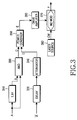
- Fig. 3 is a block diagram of a duobinary optical transmission system in accordance with a preferred embodiment of the present invention.
- the duobinary optical transmission system includes a conventional: (1) driver 360, (2) Mach-Zehnder-interferometer-type optical intensity modulator (MZ MOD) 370, and (3) laser source 380 for generating a carrier wave.
- MZ MOD Mach-Zehnder-interferometer-type optical intensity modulator
- the duobinary optical transmission system according to the present invention does not use a precoder using a feedback loop and an electric LPF. Instead, the present invention uses a single Toggle Flip-Flop (T.FF) 310, a delay 320, an AND gate 330, an attenuator 340, and a power combiner 350.
- T.FF Toggle Flip-Flop
- Fig. 4 is a timing diagram of output signals at nodes A ⁇ F shown in Fig. 3. Operations and signal flows of the duobinary optical transmission system will hereinafter be described with reference to Figs. 3 ⁇ 4.
- a two-level data signal A to be transmitted is applied to the T.FF 310.
- An inverted two-level data signal A (an inverted signal of the signal A) is applied to a delay 320.
- a toggled signal B is generated at every rising edge of the data signal A by the T.FF 310.
- the data signal A and the output signal B of the T.FF 310 are applied to the AND gate 330, and then the AND gate 330 generates a signal C.
- the T.FF 310 and the AND gate 330 are adapted to separate a group of '1' from the data signal.
- the T.FF 310 and the AND gate 330 separate an odd-th (or even-th) 1 group from the data signal in such a way that the odd-th (or even-th) 1 group is at a high level, the even-th (or odd-th) 1 group is at a low level, and a signal '0' is at an intermediate level.
- the attenuator generates a signal D for reducing intensity of the output signal of the delay 320 by half, and outputs the signal D to a power combiner 350.
- the delay 320 is adapted to enable the attenuator 340's output signal D and the AND gate 330's output signal C to be aligned in phase at the power combiner 350 in consideration of a self-delay value of the T.FF 310 and the influence of the AND gate 330.
- the output signal C of the AND gate 330 and the output signal D of the attenuator 340 are added by the power combiner 350 in such a way that the initial two-level signal is converted into a three-level signal at the power combiner 350.
- the three-level signal is applied to a drive amplifier 360.
- the drive amplifier 360 outputs it to the MZ MOD 370 as a driving signal in such a way that a carrier wave received from the laser source 380 is modulated into a two-level optical signal at the MZ MOD 370.
- this single output signal is adapted as a driving signal for a single arm MZ modulator with a single electrode.
- the first and second output signals are adapted as driving signals for a dual arm MZ modulator with a dual electrode.
- Fig. 5 is a block diagram of a duobinary optical transmission system in accordance with another preferred embodiment of the present invention.
- the duobinary optical transmission system includes a convention (1) Toggle Flip-Flip (T.FF) 510, (2) delay 520, (3) AND gate 530, (4) drive amplifier 550, (5) Mach-Zehnder-interferometer-type optical intensity modulator (MZ MOD) 560, and (6) laser source 570.
- T.FF Toggle Flip-Flip
- MZ MOD Mach-Zehnder-interferometer-type optical intensity modulator
- the duobinary optical transmission system in accordance with another preferred embodiment of the present invention does not use an inverted data signal /Q and an attenuator for reducing intensity of the inverted data signal /Q.
- the present invention uses an adder 540 instead of a power combiner as shown in Fig. 3.
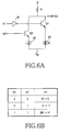
- Fig. 6a is a detailed circuit diagram of the adder shown in Fig. 5.
- Fig. 6b is a logical truth table related to input signals of the adder shown in Fig. 6a.
- a first input signal in1 denotes a reference character '+' shown in Fig. 5, and a second input signal in2 denotes a reference character '-' shown in Fig. 5.
- the first input signal in1 is logically inverted by an inverter, and is input to the base of the first transistor Q1.
- the second input signal in2 is input to the base of the second transistor Q2.
- the first and second transistors Q1 and Q2 connect their own emitter to current sources 62 and 63, respectively.
- a current magnitude of the current source 62 connected to the emitter of the first transistor Q1 is double that of the other current source 63 connected to the emitter of the second transistor Q2.
- a collector of each transistor is connected to the load resistor R.
- One of current values 0, i, and 2i may be applied to the load resistor R according to an ON or OFF state of each transistor.
- output voltages of the adder become signals '0', 'iR', and '2iR'.
- each transistor when an input signal '1' is applied to each transistor, each transistor is turned off such that current is not applied thereto.
- each transistor When an input signal '0' is applied to each transistor, each transistor is turned on such that a current from each current source is applied thereto.
- the first and second input signals are respectively at a logical level '1', they are inverted to a logic level '0' by an inverter, and the logic level '0' is applied to the first transistor Q1 and the logic level '1' is applied to the second transistor Q2. Therefore, the first transistor Q1 is only turned on such that a current of 2i is applied to the load resistor R and an output voltage of the adder becomes a signal of 2iR.
- the second transistor Q2 is only turned on such that a current of i is applied to the load resistor R and an output voltage of the adder becomes a signal of iR.
- Fig. 6b is a logical truth table related to input signals in1 and in2 of the adder shown in Fig. 6a.
- a signal 2iR may be represented as a logic level '+1'
- a signal of iR may be represented as a logic level '0'
- a signal of 0 may be represented as a logic level '-1'.
- the first input signal in1 is at a logic level '1' and the second input signal in2 is at a logic level '0' in the adder 540 shown in Fig. 5.
- Fig. 7 is a view illustrating signal waveforms at nodes A ⁇ C and G ⁇ I shown in Fig. 5. Operations and signal flows of the duobinary optical transmission system will hereinafter be described with reference to Figs. 5 and 7.
- the operations at nodes A ⁇ C are similar to those of Fig. 3 such that signal waveforms A ⁇ C shown in Fig. 7 are similar as those of Fig. 5.
- An output signal C of an AND gate 530 and an output signal G of a delay 520 are applied to an adder 540 such that the adder 540 generates a three-level signal H.
- the three-level signal H is amplified by a drive amplifier 550, and the amplified three-level signal H is applied to the MZ MOD 560 as a driving signal.
- this single output signal is adapted as a driving signal for a single arm MZ modulator with a single electrode.
- the drive amplifier 550 generates a first output signal and a second output signal being an inverted signal of the first output signal
- the first and second output signals are adapted as driving signals for a dual arm MZ modulator with a dual electrode.
- Fig. 8 is a view illustrating a duobinary optical signal modulation procedure at a Mach-Zehnder-interferometer-type optical intensity modulator (MZ MOD).
- a three-level signal E shown in Fig. 3 or a three-level signal H (again as shown in Fig. 3) are respectively applied to a MZ MOD such that the MZ MOD generates a duobinary optical signal F having a phase difference of 180 degrees ( ⁇ ).
- a bias of the MZ MOD is positioned at a null point of a MZ MOD's characteristic curve.
- a duobinary optical transmission system uses the crossed phase characteristics of a duobinary signal without using a feedback-type precoder and an electric LPF, and is thereby not affected by PRBS. Also, the duobinary optical transmission system is very resistant to wavelength division characteristics, thereby increasing a transmission distance as well as improving a transfer rate.
Landscapes
- Physics & Mathematics (AREA)
- Electromagnetism (AREA)
- Engineering & Computer Science (AREA)
- Computer Networks & Wireless Communication (AREA)
- Signal Processing (AREA)
- Optics & Photonics (AREA)
- Optical Communication System (AREA)
Abstract
Description
This object is solved by the subject matter of the independent claims. Preferred embodiments are defined in the dependent claims.
Claims (20)
- A duobinary optical transmission apparatus comprising:an optical modulator that receives a two-level data signal, the optical modulator including,a toggle device to generate a toggled signal at every rising edge of the two-level data signal;a logic AND device to generate an ANDed signal of the two-level data signal and toggled output signal; anda combiner configured for generating a three-level signal by combining the ANDed signal and a delayed data signal which is based on said two-level data signal.
- The duobinary optical transmission apparatus as set forth in claim 1, wherein the data signal is an inverted signal of said two-level data signal.
- The duobinary optical transmission apparatus as set forth in claim 1, wherein the data signal is said two-level data signal.
- The duobinary optical transmission apparatus as set forth in one of claims 1 to 3, wherein said optical modulator is for generating a modulated optical signal made by a modulation of an optical carrier wave.
- The duobinary optical transmission apparatus as set forth in one of claims 1 to 4, wherein the toggle device is a T flip-flop.
- The duobinary optical transmission apparatus as set forth in claim 5, wherein the T flip-flop is adapted for receiving the two-level data signal.
- The duobinary optical transmission apparatus as set forth in claim 5 or 6, wherein the T flip-flop and the logic AND device separate an odd-th or even-th 1 group from the input two-level data signal in such a way that the odd-th or even-th 1 group is at a high level, the even-th or odd-th 1 group is at a low level, and a signal '0' is at an intermediate level.
- The duobinary optical transmission apparatus as set forth in claim 7, wherein the 1 group of the separated data signal includes signals having a phase difference of 180 degrees (π) therebetween.
- The duobinary optical transmission apparatus as set forth in one of claims 1 to 8, wherein the logic AND device is an AND gate for performing an AND operation on said two-level data signal and said toggled output signal.
- The duobinary optical transmission apparatus as set forth in one of claims 1 to 9 further comprising a delay for delaying the data signal based on said two-level data signal and providing a delayed output signal.
- The duobinary optical transmission apparatus as set forth of claim 10 further comprising an attenuator for reducing intensity of the delayed output signal.
- The duobinary optical transmission apparatus as set forth in one of claims 1 to 11, wherein the combiner is a power combiner.
- The duobinary optical transmission apparatus as set forth in claim 11 or 12, wherein said combiner is for generating said three-level signal by adding the ANDed signal of the two-level data signal and an output signal of the attenuator.
- The duobinary optical transmission apparatus as set forth in claims 11 or 13, wherein the attenuator is for reducing intensity of the delayed output signal by substantially half.
- The duobinary optical transmission apparatus as set forth in one of claims 1 to 14 further comprising an adder for generating a three-level signal by adding an output signal of the AND gate and an output signal of the delay.
- The duobinary optical transmission apparatus as set forth in claim 15, wherein the adder includes:an inverter for inverting an output signal of the AND gate;a first transistor for connecting its own base to an output terminal of the inverter, and forming a collector-emitter current path between a load resistor and a first current source; anda second transistor for connecting its own base to an output terminal of the delay, and forming a collector-emitter current path between the load resistor and a second current source, wherein a current magnitude of the first current source is double that of the second current source.
- The duobinary optical transmission apparatus as set forth in one of claims 1 to 15, further including:a modulator driving signal generator to generate a modulator driving signal using the three-level signal;a light source to generate an optical carrier wave;and an interferometer-type optical modulator to modulate the carrier wave into a two-level optical signal according to the modulator driving signal.
- The duobinary optical transmission apparatus as set forth in one of claims 1 to 17, wherein the optical modulator is a Mach-Zehnder-interferometer-type optical intensity modulator (MZ MOD) having one or two electrodes.
- The duobinary optical transmission apparatus as set forth in one of claims 1 to 18 further including a means for modifying the ratio of intensity of the delayed signal and the ANDed signal.
- An operation method adapted to operate the apparatus according to one of claims 1 to 19.
Applications Claiming Priority (2)
| Application Number | Priority Date | Filing Date | Title |
|---|---|---|---|
| KR2002073407 | 2002-11-25 | ||
| KR10-2002-0073407A KR100469710B1 (en) | 2002-11-25 | 2002-11-25 | Optical duobinary transmitter |
Publications (3)
| Publication Number | Publication Date |
|---|---|
| EP1422842A2 true EP1422842A2 (en) | 2004-05-26 |
| EP1422842A3 EP1422842A3 (en) | 2005-10-12 |
| EP1422842B1 EP1422842B1 (en) | 2007-02-07 |
Family
ID=32226345
Family Applications (1)
| Application Number | Title | Priority Date | Filing Date |
|---|---|---|---|
| EP03017118A Expired - Lifetime EP1422842B1 (en) | 2002-11-25 | 2003-07-28 | Duobinary optical transmission apparatus |
Country Status (6)
| Country | Link |
|---|---|
| US (1) | US7362978B2 (en) |
| EP (1) | EP1422842B1 (en) |
| JP (1) | JP3940117B2 (en) |
| KR (1) | KR100469710B1 (en) |
| CN (1) | CN1503499A (en) |
| DE (1) | DE60311626T2 (en) |
Cited By (1)
| Publication number | Priority date | Publication date | Assignee | Title |
|---|---|---|---|---|
| CN109412699A (en) * | 2018-11-28 | 2019-03-01 | 武汉邮电科学研究院有限公司 | Pulse generation method, device, coherent phase sensitivity time domain reflection method and system |
Families Citing this family (2)
| Publication number | Priority date | Publication date | Assignee | Title |
|---|---|---|---|---|
| KR100532305B1 (en) * | 2003-09-09 | 2005-11-29 | 삼성전자주식회사 | Duobinary optical transmitter |
| KR100651378B1 (en) * | 2004-10-20 | 2006-11-29 | 삼성전자주식회사 | Concubine Young-Return-Alternative Sign Inverting |
Family Cites Families (14)
| Publication number | Priority date | Publication date | Assignee | Title |
|---|---|---|---|---|
| US3233236A (en) * | 1961-06-28 | 1966-02-01 | Lear Siegler Inc | System for bandwidth compression of binary signals |
| US3162724A (en) * | 1961-07-03 | 1964-12-22 | Otmar E Ringelhaan | System for transmission of binary information at twice the normal rate |
| US3337864A (en) * | 1963-08-01 | 1967-08-22 | Automatic Elect Lab | Duobinary conversion, reconversion and error detection |
| US3517117A (en) * | 1968-01-24 | 1970-06-23 | Southern Pacific Transport Co | Bandwidth reduction coding technique |
| US3631463A (en) * | 1969-03-10 | 1971-12-28 | Sperry Rand Corp | Self-clocked encoding scheme |
| US4086566A (en) * | 1976-11-15 | 1978-04-25 | Gte Automatic Electric Laboratories Incorporated | Error detector for modified duobinary signals |
| CA1205561A (en) * | 1983-03-11 | 1986-06-03 | Kiichi Yamashita | Method of searching fault locations in digital transmission line |
| DE69531328T2 (en) * | 1994-09-12 | 2004-02-12 | Nippon Telegraph And Telephone Corp. | Intensity modulated optical transmission system |
| JP3027944B2 (en) | 1996-08-16 | 2000-04-04 | 日本電気株式会社 | Optical duobinary signal light generation method and optical transmitter |
| US5892858A (en) | 1997-03-27 | 1999-04-06 | Northern Telecom Limited | Duobinary coding and modulation technique for optical communication systems |
| US6226114B1 (en) * | 1998-07-02 | 2001-05-01 | Scientific-Atlanta, Inc. | Temperature compensation for uncooled laser |
| JP3910003B2 (en) * | 2000-05-29 | 2007-04-25 | 富士通株式会社 | Optical receiving station, optical communication system, and dispersion control method |
| DE10040471C2 (en) | 2000-08-18 | 2002-09-19 | Siemens Ag | Encoder for a duobinary signal |
| US20030063698A1 (en) * | 2001-09-28 | 2003-04-03 | Andrew Bonthron | Optical synchronous coding system |
-
2002
- 2002-11-25 KR KR10-2002-0073407A patent/KR100469710B1/en not_active Expired - Fee Related
-
2003
- 2003-06-10 US US10/458,150 patent/US7362978B2/en not_active Expired - Fee Related
- 2003-07-28 DE DE60311626T patent/DE60311626T2/en not_active Expired - Lifetime
- 2003-07-28 EP EP03017118A patent/EP1422842B1/en not_active Expired - Lifetime
- 2003-07-30 CN CNA031523641A patent/CN1503499A/en active Pending
- 2003-11-21 JP JP2003392390A patent/JP3940117B2/en not_active Expired - Fee Related
Cited By (1)
| Publication number | Priority date | Publication date | Assignee | Title |
|---|---|---|---|---|
| CN109412699A (en) * | 2018-11-28 | 2019-03-01 | 武汉邮电科学研究院有限公司 | Pulse generation method, device, coherent phase sensitivity time domain reflection method and system |
Also Published As
| Publication number | Publication date |
|---|---|
| JP2004312679A (en) | 2004-11-04 |
| CN1503499A (en) | 2004-06-09 |
| KR100469710B1 (en) | 2005-02-02 |
| EP1422842A3 (en) | 2005-10-12 |
| DE60311626D1 (en) | 2007-03-22 |
| DE60311626T2 (en) | 2007-05-24 |
| EP1422842B1 (en) | 2007-02-07 |
| US7362978B2 (en) | 2008-04-22 |
| KR20040045584A (en) | 2004-06-02 |
| US20040101315A1 (en) | 2004-05-27 |
| JP3940117B2 (en) | 2007-07-04 |
Similar Documents
| Publication | Publication Date | Title |
|---|---|---|
| US8311416B2 (en) | Method and apparatus for generating optical duo binary signals with frequency chirp | |
| US7474858B2 (en) | Duobinary optical transmission device using at least one semiconductor optical amplifier | |
| JP3371857B2 (en) | Optical transmission equipment | |
| US7193539B2 (en) | Precoder and optical duo-binary transmission apparatus using the same | |
| US7257330B2 (en) | Duobinary optical transmission apparatus using a semiconductor optical amplifier | |
| EP1404036B1 (en) | Duobinary optical transmission apparatus | |
| US20050100346A1 (en) | Optical transmitter for use in high-density wavelength division multiplexing (WDM) optical transmission system | |
| US7206519B2 (en) | Duobinary optical transmission apparatus | |
| EP1416654B1 (en) | Duobinary optical transmission | |
| US7289048B2 (en) | Duo-binary encoder and optical duo-binary transmission apparatus using the same | |
| US7212691B2 (en) | Polarization-shaped duobinary optical transmission apparatus | |
| US20040105686A1 (en) | Optical transmission system using optical phase modulator | |
| US20050116841A1 (en) | Duo-binary encoder and optical duo-binary transmission apparatus | |
| EP1422842B1 (en) | Duobinary optical transmission apparatus | |
| JP2006033792A (en) | Duobinary optical transmission equipment | |
| US7224907B2 (en) | Duobinary optical transmission apparatus | |
| US7792433B2 (en) | System and method for generating optical return-to-zero signals with differential bi-phase shift and frequency chirp | |
| KR100547746B1 (en) | Duobinary Optical Transmitter |
Legal Events
| Date | Code | Title | Description |
|---|---|---|---|
| PUAI | Public reference made under article 153(3) epc to a published international application that has entered the european phase |
Free format text: ORIGINAL CODE: 0009012 |
|
| 17P | Request for examination filed |
Effective date: 20030728 |
|
| AK | Designated contracting states |
Kind code of ref document: A2 Designated state(s): AT BE BG CH CY CZ DE DK EE ES FI FR GB GR HU IE IT LI LU MC NL PT RO SE SI SK TR |
|
| AX | Request for extension of the european patent |
Extension state: AL LT LV MK |
|
| PUAL | Search report despatched |
Free format text: ORIGINAL CODE: 0009013 |
|
| AK | Designated contracting states |
Kind code of ref document: A3 Designated state(s): AT BE BG CH CY CZ DE DK EE ES FI FR GB GR HU IE IT LI LU MC NL PT RO SE SI SK TR |
|
| AX | Request for extension of the european patent |
Extension state: AL LT LV MK |
|
| AKX | Designation fees paid |
Designated state(s): DE FR GB |
|
| GRAP | Despatch of communication of intention to grant a patent |
Free format text: ORIGINAL CODE: EPIDOSNIGR1 |
|
| GRAS | Grant fee paid |
Free format text: ORIGINAL CODE: EPIDOSNIGR3 |
|
| GRAA | (expected) grant |
Free format text: ORIGINAL CODE: 0009210 |
|
| AK | Designated contracting states |
Kind code of ref document: B1 Designated state(s): DE FR GB |
|
| REG | Reference to a national code |
Ref country code: GB Ref legal event code: FG4D |
|
| REF | Corresponds to: |
Ref document number: 60311626 Country of ref document: DE Date of ref document: 20070322 Kind code of ref document: P |
|
| ET | Fr: translation filed | ||
| PLBE | No opposition filed within time limit |
Free format text: ORIGINAL CODE: 0009261 |
|
| STAA | Information on the status of an ep patent application or granted ep patent |
Free format text: STATUS: NO OPPOSITION FILED WITHIN TIME LIMIT |
|
| 26N | No opposition filed |
Effective date: 20071108 |
|
| REG | Reference to a national code |
Ref country code: FR Ref legal event code: PLFP Year of fee payment: 14 |
|
| PGFP | Annual fee paid to national office [announced via postgrant information from national office to epo] |
Ref country code: GB Payment date: 20160615 Year of fee payment: 14 |
|
| PGFP | Annual fee paid to national office [announced via postgrant information from national office to epo] |
Ref country code: FR Payment date: 20160615 Year of fee payment: 14 |
|
| PGFP | Annual fee paid to national office [announced via postgrant information from national office to epo] |
Ref country code: DE Payment date: 20160614 Year of fee payment: 14 |
|
| REG | Reference to a national code |
Ref country code: DE Ref legal event code: R119 Ref document number: 60311626 Country of ref document: DE |
|
| GBPC | Gb: european patent ceased through non-payment of renewal fee |
Effective date: 20170728 |
|
| REG | Reference to a national code |
Ref country code: FR Ref legal event code: ST Effective date: 20180330 |
|
| PG25 | Lapsed in a contracting state [announced via postgrant information from national office to epo] |
Ref country code: DE Free format text: LAPSE BECAUSE OF NON-PAYMENT OF DUE FEES Effective date: 20180201 Ref country code: GB Free format text: LAPSE BECAUSE OF NON-PAYMENT OF DUE FEES Effective date: 20170728 |
|
| PG25 | Lapsed in a contracting state [announced via postgrant information from national office to epo] |
Ref country code: FR Free format text: LAPSE BECAUSE OF NON-PAYMENT OF DUE FEES Effective date: 20170731 |