Field of the Invention
This invention relates to frequency generation circuits
for wireless communication units. The invention is
applicable to, but not limited to, a frequency generation
circuit that needs to function with a low phase noise.
Background of the Invention
Wireless communication units, for example those operating
in a cellular telephone system such as the Global System
for Mobile communications (GSM), use a broadcast
reference frequency signal to calibrate their operating
(transmit/receive) frequency. The broadcast signal is
generally transmit from one or more base transceiver
stations (BTSs). In this manner, the wireless
communication units use the broadcast reference frequency
signal in order to synchronise their internal frequency
generation circuits. The units synchronise their
operating frequency to match the system frequency, prior
to entering into a communication. The synchronisation
occurs when receiving a signal and when generating a
modulated signal for transmission.
The GSM standard specifies a modulation scheme of
Gaussian Minimum Shift Keyed (GMSK). Such a minimum
shift keying (MSK) modulation scheme is a subset of a
frequency shift-keying scheme (FSK). In FSK, binary data
is communicated by switching between two frequencies,
where one frequency is sent if a current data bit is a
'1' and a second frequency is sent if a current data bit
is a '0'. When the frequency deviation is set to equal
half the input serial baud rate, the modulation scheme is
termed MSK.
There are many known techniques for synthesizing
modulated signals onto frequencies for transmission. A
popular technique at present is using a fractional
division synthesizer, which enables a wide range of
discrete frequencies to be tuned to by appropriate
selection of 'division' parameters applied to a reference
oscillator.
The GSM standard also specifies a data rate of 270
kbits/sec in the transmission of speech and data signals.
To facilitate such large data rate, a large synthesizer
loop bandwidth is required. A problem in using a
fractional division synthesizer is that it is invariably
not wide enough to cover the entire modulation frequency
for both low and high frequency response in order to
handle the GMSK modulation requirements. With a typical
loop bandwidth of less than 200 kHz, the synthesizer
bandwidth is less than the modulation bandwidth. In
essence, it is therefore a narrow bandwidth synthesizer.
Modulating a signal to a single port, to give a uniform
performance for the entire GMSK bandwidth is known to be
a complex task. Alternatively, the synthesizer can be
divided into two portions, a low frequency response of
the synthesizer and a high frequency response of the VCO
that rolls off at the loop bandwidth.
One of the most commonly used techniques to enable
fractional division synthesizers to be used in
synthesizing high data rate signals is to use a two spot
modulation technique. This technique applies Modulation
to both the synthesizer loop and the voltage-controlled
oscillator (VCO), as known to those skilled in the art.
In this design, the modulation signal is applied to the
loop divider and the VCO tuning (steering) line, or loop
filter.
The loop divider is sensitive only to the signal
frequencies below the loop bandwidth. The VCO is
sensitive only to signal frequencies above the loop
bandwidth. Thus, at around the loop bandwidth the
modulation signal is sensitive to both the loop divider
as well as the VCO, where the resultant response of the
modulation signal is the sum of the VCO response and the
loop response.
Low frequency modulation is applied to the loop divider
rather than the more conventional method of phase
modulation to facilitate digital modulation. The digital
modulation method allows for very low frequency
modulation, down to DC level, which is normally not
possible with the well-known reference modulation method.
Modulation frequencies above the loop bandwidth of 150
kHz must be applied to the VCO for FM modulation.
Typically, the high frequency components of the GMSK
modulating signal are applied to the VCO via an on chip
programmable attenuator. The output of the modulation
attenuator is applied to the VCO modulation port.
In a GMSK modulator, the input signal is differentially
encoded and mapped to '+1' or '-1' in a frequency shift
keyed manner and pre-filtered with a digital Gaussian
filter, to reduce the distortion resulting from the bit
transitions and produce a GMSK modulated signal. The
filtering may be performed using a read-only memory (ROM)
look up filter. When applied in a dual-port modulator
technique, the filtered signal is then used to modulate a
fractional 'N' synthesizer (Direct Port), where it is
filtered again by the synthesizer closed loop response,
as known to those skilled in the art.
It is also known that the filtered signal may be routed
to an analogue to digital converter (A/D). The A/D
output is then attenuated and passed to the voltage
controlled oscillator (VCO) steering line. The signal
from the dual-port is filtered by high pass filter.
Combining both signals, from the dual-port and the direct
port, yields the desired GMSK signal.
A significant advantage of a dual-port technique is the
ability to establish low phase noise at the synthesizer
level. The level of phase noise is typically of the
order of -121 dBc/Hz @ 400 kHz away from the centre
frequency. In this regard, phase detector noise must be
attenuated. The phase noise is thus attenuated whilst
preserving a high quality generated GMSK signal in terms
of root mean square (RMS) phase error. A typical phase
error RMS value is approximately 1.1 degrees.
A key factor in the design of a dual-port modulator is in
obtaining a flat modulation response from DC to 300 kHz.
In this regard, it is important to select how and where
the modulation signal is applied to the VCO.
One known method is to apply the modulation signal
directly to the VCO steering line via a small capacitor.
This method has the problem of unbalanced zeroes and
poles due to the loop filter. As such, it requires a
separate, undesirable pole/zero cancellation network to
achieve modulation flatness.
Another method is to apply the modulation signal to a
loop filter via a resistive voltage divider. This method
should give a flat modulation response without a
pole/zero compensation network. However, this
implementation requires a coupling capacitor to provide
for direct current (DC) blocking from the modulation
attenuator buffer output. This DC blocking capacitor has
the potential problem of introducing undesirable DC
transients on very low frequency components. Also, the
resistive divider potentially provides a leakage path for
the loop capacitor to cause an apparent increase in
synthesizer settling time.
An alternative method is to use a capacitive attenuator
network to couple the modulating signal into the loop
filter.
However, the inventors of the present invention have
recognised a number of disadvantages with such a dual-port
modulator technique. In particular, in order to
minimise phase error RMS and peak phase error of the
transmitted signal, it is critical that attenuation
balancing is performed between the direct port and the
dual-port of the dual-port modulation input.
The current technique to achieve balancing of the dual-port
signals is to measure the VCO RMS during factory
tuning and manually tune the VCO sensitivity response.
This is a very time-consuming exercise. It is also an
inflexible solution as, once tuned, there is no mechanism
for re-tuning apart from returning the unit to the
factory.
A primary focus of the present invention was to produce a
GSM transmitter that is based on dual-port modulation and
a capacitance divider arrangement for coupling the input
signal to the modulator. To maintain low cost, the
transmitter needs to generate with a reduced voltage
controlled oscillator (VCO) sensitivity specification in
terms of component tolerances, (i.e. KV Min/KV Max = 20%
~ 30 %), in order to facilitate a simple and inexpensive
transmitter design.
Thus, a need has arisen to provide a wireless
communication unit, and in particular, a method of
selecting and controlling appropriate attenuation values
in a VCO dual-port modulation circuit, wherein the
aforementioned disadvantages may at least be alleviated.
Statement of Invention
In accordance with a first aspect of the present
invention, there is provided a wireless communication
unit, as claimed in Claim 1.
In accordance with a second aspect of the present
invention there is provided a method of tuning a
frequency of a wireless communication unit, as claimed in
Claim 6.
In accordance with a third aspect of the present
invention, there is provided a storage medium storing
processor implementable instructions or associated data,
as claimed in Claim 11.
Further aspects of the present invention are defined in
the dependent Claims.
Brief Description of the Drawings
Exemplary embodiments of the present invention will now
be described, with reference to the accompanying
drawings, in which:
Description of Preferred Embodiments
In the context of the present invention, the inventors
determined that attenuation/level balancing in a dual-port
modulator depends on the following characteristics:
In order to quantify the sensitivity requirements of a
dual-port modulator, simulations were performed to
determine the VCO's phase error RMS sensitivity to dual-port
balancing/mismatching. It was determined that a +/-2dB
difference between the ports resulted in a phase
error RMS of approximately five degrees. The effect of
dual-port balancing/mismatch sensitivity on phase error
margin variation on the balancing was then estimated.
The results are indicated in FIG. 1, where graphs of
received dual-port constellations are illustrated. A
first graph 100 indicates the simulated phase error
mismatch of 0.23dB compared to a simulated phase error
mismatch of 1.5dB in the second graph 110. As shown in
the second graph 110, a mismatch of 1.5 dB is acceptable.
Referring now to FIG. 2, the effect of the transmitted
signal quality in terms of phase error RMS and peak is
illustrated. In particular, a range of closed loop
responses are shown for various mismatches (in dB),
plotted against the total transfer function magnitude.
As shown, a mismatch of approximately 1.5dB causes a peak
phase error of approximately 2dB and a phase error RMS
performance of approximately 1dB. FIG. 2 illustrates
clearly, why dual port balancing is required. Any
mismatch in the dual-port levels will result in an
undesired close loop response, which will cause phase
error RMS degradation. Thus, the inventors of the
present invention have determined that balancing is
required on the DAC output. This balancing is effected
in the form of Voltage Attenuation, using an attenuator,
the operation of which is described later with regard to
FIG. 4, FIG. 5 and FIG. 6. The amount of attenuation
required, i.e. the level of balancing to counteract the
mismatch, is dependent upon the phase error RMS.
Referring now to FIG.3, a graph illustrates the estimated
phase error RMS and peak phase error versus dual-port
mismatch. It is clear from FIG. 3 that in order to
maintain sufficient GMSK signal quality in terms of phase
error, a worst-case dual-port mismatch of +/- 1.5dB is
desired. It is notable that the phase error RMS and peak
phase error is not symmetric dependent upon the level of
dual-port attenuation mismatch. Furthermore, it is noted
that increasing the phase margin will result in improved
attenuation mismatch sensitivity.
VCO sensitivity and loop tolerances can cause undesired
mismatch, as shown in equation [22] below. It is
important to estimate the amount of dual-port balancing
that will still insure desired phase error RMS and phase
error peak. The mismatch sensitivity is related to the
phase margin and the closed loop bandwidth of the direct
port. Those parameters need to be carefully controlled
in order to achieve the desired adjacent channel phase
noise performance.
It was further determined by the inventors that by
increasing the VCO's loop phase margin from fifty degrees
to approximately sixty degrees, resulted in an
improvement in the balancing margin of approximately 2dB
and approximately five degrees of phase error RMS.
Furthermore, increasing the phase margin resulted in a
decreased adjacent channel power (ACP) performance of 3dB
at 400 kHz from the centre frequency, i.e. -70dB to
-67dB. From these calculations, it can be determined that
it is necessary to lower the (worst-case) sensitivity
mismatch to approximately +/- 1dB. The inventors of the
present invention also determined that the total
attenuation required in order to achieve balancing is
-43.03 dB, for a typical VCO sensitivity of 24 MHz/V.
A major factor in such VCO designs is the use of low
tolerance components to keep costs low. For example, it
is typical for manufacturers to design VCO circuits with
transmit VCO sensitivity tolerances of around 20% with
loop filter component tolerances of 5%. Thus, with such
tolerance values, the inventors of the present invention
determined that the worst-case attenuation mismatch could
be +/-3.2dB in terms of phase error RMS and adjacent
channel power (ACP). It is therefore clear that using
typical tolerance values for the loop filter components
is insufficient to achieve the required sensitivity
performance in a dual-port modulation scheme.
Thus, the inventors of the present invention have
developed the following equation in order to set the
desired attenuation/magnitude in the dual-port modulator:
Internal Atten. [dB] + Capacitance Divider Attenuation
[dB] = F (VCO Sensitivity, D/A Output Voltage)
By simulating a dual-port modulator, it was determined
that the capacitance divider attenuation needs to be
-36.8dB. The total desired attenuation could be estimated
for specific VCO sensitivity values. Table 1 presents
the total desired attenuation versus a typical VCO of 24
MHz/V for different sensitivity tolerances.
| Total desired attenuation versus sensitivity tolerance |
| VCO SENSITIVITY TOLERANCES % | MIN TOTAL ATTENUATION [DB] | MAX TOTAL ATTENUATION [DB] | VCO SENSITIVITY MARGIN [MHZ/V] |
| 1 | -42.945 | -43.119 | +/- 0.24 |
| 2 | -42.857 | -43.204 | +/- 0.48 |
| 3 | -42.76 | -43.303 | +/- 0.72 |
| 4 | -42.678 | -43.37 | +/- 0.92 |
| 5 | -42.587 | -43.456 | +/-1.2 |
| 10 | -42.117 | -43.86 | +/- 2.4 |
| 20 | -41.094 | -44.616 | +/- 4.8 |
| Capacitance divider attenuation, versus loop filter component tolerances. |
| LOOP FILTER COMPONENTS TOLERANCES % | MIN ATTENUATION [DB] | MAX ATTENUATION [DB] |
| 2 | -36.46 | -37.14 |
| 5 | -35.95 | -37.66 |
Returning to equation [1], for capacitance divider
attenuations, results in the following definitions:
Max. atten. = Max. Total atten. - Min. CA
Min. atten. = Min. Total atten. - Max. CA
Effective Mismatch = Max. atten. - Min. atten.
Where:
CA = Capacitance Attenuation [dB]
| Effective Maximum Mismatch [dB] |
| TOLERANCE [LOOP FILTER, VCO SENSITIVITY] | MAX. INTERNAL ATTENUATION [DB] | MIN. INTERNAL ATTENUATION [DB] | EFFECTIVE MISMATCH [DB] |
| [5%, 5%] | -7.51 | -4.927 | +/- 1.3 |
| [2%, 5%] | -6.996 | -5.44 | +/- 0.78 |
From Table 3, it can be clearly seen that using
capacitance divider loop filter components with
tolerances of 2%, together with a VCO sensitivity of 5%,
results in an effective attenuation mismatch of +/- 0.78
dB. The inventors of the present invention determined
that this level of performance, when used in conjunction
with a VCO sensitivity/tuning algorithm, is sufficient
for the dual-port modulator. Thus, the VCO
sensitivity/tuning algorithm focus is to monitor the VCO
sensitivity to within +/- 1 MHz/V.
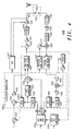
Referring now to FIG. 4, a block diagram of a wireless
subscriber communication unit/mobile station (MS) 400,
adapted to support the inventive concepts of the
preferred embodiments of the present invention, is
illustrated. The wireless communication unit 400
includes a digital signal processor (DSP) 402 that
transmits '0's/'1's binary data via a line identified by
'STD', and receives '0's/'1's binary data via a line
identified by 'SRD'. The DSP 402 inputs binary data to a
radio frequency (RF) modulator/demodulator (MODEM)
function 404.
In a transmit (TX) mode of operation, the RF MODEM 404 is
used for synthesizing the GMSK signal and modulating the
TX VCO. In a receive (RX) mode of operation, the RF
MODEM 404 is used for back-end demodulation.
The RF MODEM 404 outputs a synthesized GMSK signal to a
dual-port loop filter 406. This filter is used for both
a direct-port and a dual-port of the VCO design of the
present invention, i.e. the direct port uses an 'up'.
(high-frequency response) pin, and the dual-port uses a
'down' (low-frequency response) pin. The dual-port loop
filter 406 outputs a filtered signal to a TX VCO circuit
402. The TX VCO circuit 402 is modulated to the desired
RF frequency, using the direct and dual port directly.
The TX VCO circuit 402 is fed to a driver function 410,
which is a first stage amplifier and buffer used for TX
VCO isolation. The driver function 410 outputs a signal
to a filter 412 that filters harmonics, and thereafter to
the RF power amplifier (PA) 414. The RF PA is the main
RF power amplifier used to achieve the desired output
signal power. The high-power RF signal is fed to a
coupler 464 that couples the RF signal to the power
amplifier control (PAC) 462 for control analysis. The
PAC 462 controls the power level and the time ramp-up and
ramp-down of the transmitted signal. The high-power RF
signal is input to an antenna switch 416, which performs
the RF switching between TX and RX modes of operation for
time division multiplexing.
In a RX mode of operation, a received signal is routed
from the antenna switch 416 to a Front-end Filter 418.
The Front-end Filter 418 is the first RF stage in the
receiver and filters the image and half-IF spurs, as
known to those skilled in the art. The front-end
filtered signal is input to a Low Noise Amplifier (LNA)
420, where it is amplified and input to a Mixer 424 that
translates the received frequency to an intermediate
frequency (IF). The IF signal is input to a filter and
balun 426, which is used for IF filtering and filtering
the received channel, as known to those skilled in the
art.
With regard to the frequency generation and control
circuitry, a reference local oscillator (TCXO) 428 is
used for the RF and Digital circuits. An analogue to
digital converter function (GCAP A/D) 430 is used for
sampling the TX VCO sensitivity for dual port processing,
in accordance with the preferred embodiment of the
present invention. A low-noise local oscillator (RX VCO)
432 is configured to operate at an IF frequency above the
received frequency band. In a GSM unit, this is
typically arranged to be a frequency of 26 MHz. A RX
loop filter 434 is used for the main RX loop dynamics and
filtering spurs and noise. In a GSM unit, this is
typically configured to be 60 KHz in order to achieve the
necessary lock time. A second local oscillator (LO) VCO
236 is used translate the IF frequency to base band at
mixer 454, after the received filtered signal has been
amplified by pre-amplifier 452. The pre-amplifier
introduces high gain to the received signal in order to
achieve the desired dynamic range. A second LO loop
filter 438 ensures that a single-tone oscillator signal
appears in the IF frequency. The received base band
signal output from mixer 454 is amplified in base band
amplifier 456 and filtered in base band filter 458,
before being sampled in the receiver analogue-to-digital
converter (RX A/D) 460, to produce a digital received
signal for processing by DSP 402.
A phase detector 440 in the RF MODEM 404 detects the
phase difference between the divided TX VCO 402 and the
TCXO 428 reference signal. A charge pump 442 introduces
current into, or out of, the loop filter 406, in
proportion to the detected phase difference. A loop
divider 444 divides the frequency from the TX VCO 402 to
match the reference signal frequency.
In particular, in accordance with the preferred
embodiment of the present invention, a dual-port digital
to analogue (D/A) converter 446 converts the digital
filtered signal to an analogue signal, in order to
modulate the TX VCO signal using the dual port. The
dual-port digital signal has been pre-filtered by GMSK
filter 448, with a bandwidth of BT = 0.3. This ensures
that differential encoding, mapping and filtering is
performed.
Notably, in accordance with the preferred embodiment of
the present invention, a dual-port attenuator 450 is used
for amplitude balancing between the direct port and dual-port.
The DSP 402 controls the attenuator value.
In accordance with a preferred embodiment of the present
invention, the frequency generation circuitry has been
adapted so that it is able to use low tolerance
components. Furthermore, the DSP 402 performs an
attenuation-tuning algorithm. In this manner, the two
output signals from the dual-port modulator are
substantially balanced, as attenuator 450 controls the
dual-port signal level.
Clearly, for other wireless communication products, other
circuit configurations may be used. Furthermore, a
skilled artisan will appreciate that the DSP 402 may be
located in a different position and function in a
different manner to that shown.
The DSP 402 has also been adapted to include a look-up
table that stores attenuator settings to be used to
attenuate DAC output signals. Preferably, the look-up
table stores attenuator settings for distinct transmitter
channel frequency ranges for the wireless communication
unit 400, as shown in Table 3 below. In this manner, the
DSP 402 selects an attenuator setting to ensure a
balanced output from the dual-port modulator based upon a
frequency or frequency range used by the transmitter.
Of course, the various components within the wireless
communication unit 400 may be realised in discrete or
integrated component form. Furthermore, it is within the
contemplation of the invention that the wireless
communication unit 400 may be any wireless communication
device, such as a portable or mobile PMR radio, a mobile
phone, a personal digital assistant, a wireless laptop
computer, etc.
More generally, any re-programming or adaptation of one
or more software algorithms or data banks of the DSP 402,
may be implemented in any suitable manner. For example,
a new signal processor function or memory device may be
added to a conventional wireless communication unit 400.
Alternatively, existing parts of a conventional wireless
communication unit may be adapted, for example by
reprogramming one or more processors therein. As such,
the required adaptation may be implemented in the form of
processor-implementable instructions stored on a storage
medium, such as a floppy disk, hard disk, PROM, RAM or
any combination of these or other storage multimedia.
The preferred embodiment of the present invention is
described with reference to the GSM standard. However,
it is within the contemplation of the invention that the
inventive concepts described herein equally apply to any
wireless communication system.
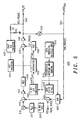
Referring now to FIG. 5, the dual-port modulator 404
adapted in accordance with the preferred embodiment of
the present invention is shown in greater detail. In the
dual-port modulator 404, binary input data is generated
by data generator 570 in a series of '0's and '1's. This
input data is differentially encoded and mapped 565 to
'+1' or '-1' in a frequency shift keyed manner, prior to
digital Gaussian filtering 448 with a 3dB bandwidth of
BT=0.3, as known to those skilled in the art.
The filtered signal is then used to modulate a signal
generated by a fractional synthesizer (505, 510, 515)
input to the Direct Port, where it is filtered again by
the synthesizer close loop response, as known to those
skilled in the art. In order to achieve the desired
phase noise at the synthesizer output, the phase detector
noise must be attenuated. This causes the GMSK signal to
be high frequency filtered. The filtered GMSK signal can
be compensated using a 'Dual-port' high pass filter 406.
It is envisaged that the filtered signal may also be
routed to an analogue to digital converter (A/D). The
A/D output is attenuated and passed to the voltage
controlled oscillator (VCO) steering line. A high-pass
filter filters the signal from the dual-port. Combining
both signals form the dual-port and the direct port
yields the desired GMSK signal. An analogue to digital
converter (A/D) 430 is used to sample the voltage at the
VCO steering line, while changing the transmitted
channel. The A/D 430 is operably coupled to a host
microprocessor, for example DSP 402 of FIG. 4, so that
the sampled values can be processed and attenuator values
stored in memory. As the transmit channel of the
wireless communication unit is known at any point in
time, the VCO sensitivity for that channel can be
estimated. During factory set-up of the wireless
communication unit, the desired attenuation for each of
the transmit channels is calculated. This information is
preferably stored in a memory element operably coupled to
DSP 402 as an array indicating variable attenuator
values. A preferred list of suitable attenuator values
is illustrated in Table 3.
The synthesized GMSK signal is passed through a 9-bit DAC
446. Notably, in accordance with the preferred
embodiment of the present invention, the DAC output
signal is attenuated using the variable attenuator 450.
This signal is convolved with the dual-port closed loop
transfer function 530, namely H(s) = Wvco/Vdac.
Thus, in FIG. 5, the two close loop transfer functions
(Direct and Dual) are estimated. The amplitude balance
between the two functions can be achieved using equation
[21], as explained below. The following set of equations
is included to indicate to a skilled artisan the theory
behind the dual-port modulator of the preferred
embodiment of the present invention.
A superposition model is used to estimate the balance
criteria, in terms of the desired attenuation, delay and
phase response.
- Note:
- K 0 - is the VCO Sensitivity [MHz/V]
-
- ICP - is the charge pump current [mA]
KV = 2πK 0
K = ICP 2π
ΔΘ VCO1 S ΔΘ dev S = Ψ1(S)⇒SΔΘ VCO1(S) = Ψ1(S)·SΔΘ dev (S)
Δω VCO1 = 2πΨ1(S)·Δfdev (S)
ΔΘ VCO2 S ΔV _ TUNE S = Ψ2 S
ΔV _ TUNE S ΔV ATT S = K S
ΔVATT ΔVDAC = ATT
ΔΘ VCO2 (S) = Ψ2(S)·K(S)·ATT ·ΔVDAC (S)
ΔΘ VCO1 S ΔΘ dev S = ψ1(S) = - β S A OL S N ch 1 + β S A OL S
Where :
β(S)A OL(S) = K H S KV SN ch
ΔωVCO1 = - 2πβ S A OL S ·N ch ·Δf DEV S 1 + β S AOL S
ΔωVCO S ΔV _TUNE S = Ψ21(S) = KV 1 + KV H S K SN ch
In order to achieve balance :
Δωvc02 (S)| S = jw = w UNITY = Δω VC 01(S)| S = jw UNITY
Note at
W UNITY ·|β(S)AOL (S)|= 1
|- 2π ·Nch ·Δfdev |≈|2πK0 K(S)ATT ·ΔVDAC (S)|
ATT · KS = N ch · Δf dev max K 0 V DAC Peak
The operation of the second port is illustrated in
equation [9]. Noting that the VCO max deviation due to
fractional deviation is +/- 67.708 kHz, it is possible to
calculate the total desired attenuation using equation
[21], which yields:
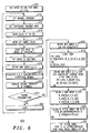
Referring now to FIG. 6, a flowchart 600 of the preferred
dual-port modulator's attenuator tuning algorithm is
illustrated. The flowchart commences in step 605 with
the radio entering a GSM test mode. A counter 'p' is
initialised to control the location of stored attenuator
values for subsequent retrieval. A first channel
frequency is then set, in step 610. The test mode then
moves to a continuous transmit mode of operation with
this channel frequency in step 615. A delay of, say, 0.5
seconds is introduced in step 620, as the group delay
between the ports is not equal. The generated channel
frequency is then sampled at step 625, and the sampled
value stored in step 630 in an array (identified as A_D)
at a location I.
The radio unit then enters an idle mode of operation in
step 635. A new array (identified as A_D_V) is defined
at step 640 and the attenuation values calculated for
respective locations in the array at step 645, where:
A_D_V[I]=((HEX2DEC(A_D)/ADSTEP)*RES)/RESDIV
Where:
RES = A/D Resolution
RESDIV = A/D Resistor Voltage Ratio
ADSTEP = A/D No. of steps
This equation is used for estimating the sampled dual-port
modulator voltage.
After calculating the attenuation value for this
location, the channel frequency being sampled is
increased, by say ten channels, as shown in step 650. If
the channel frequency has not reached or exceeded the
last frequency, say frequency no. '122' in step 655, the
counter is increased in step 660. The process then
repeats for this new channel frequency, from step 610,
until the array is complete and the final channel
frequency has been reached, in step 655.
At this stage, a new array for K_V is defined for VCO
sensitivity, in step 665. A program loop is then
commenced in step 670. A new array K_V_A for VCO
sensitivity average using, say, a 3-tap comb filter is
generated in step 675. A new array K_VCO is then defined
in step 680. The attenuation values from the array are
then calculated in step 685, for particular frequency
ranges. The attenuation values are then stored as a
table in a storage memory within the communication
device, as shown in step 690. A typical table, i.e. a
set of attenuation bits, according to the preferred
embodiment of the present invention is illustrated in
Table 4.
The algorithm supports a +/- 3.5dB mismatch, and
therefore the attenuation bits related to say, an
attenuation value of 6dB, 7dB and 8dB, are relevant.
| Attenuation bit values versus determined Attenuation value (dB) |
| MOD_ATTEN BITS | ATTENUATION VALUE (dB) |
| 4 | 3 | 2 | 1 | 0 |
| 0 | 1 | 0 | 1 | 1 | 10.0 |
| 0 | 1 | 1 | 0 | 0 | 9.5 |
| 0 | 1 | 1 | 0 | 1 | 9.0 |
| 0 | 1 | 1 | 1 | 0 | 8.5 |
| 0 | 1 | 1 | 1 | 1 | 8.0 |
| 1 | 0 | 0 | 0 | 0 | 7.5 |
| 1 | 0 | 0 | 0 | 1 | 7.0 |
| 1 | 0 | 0 | 1 | 0 | 6.5 |
| 1 | 0 | 0 | 1 | 1 | 6.0 |
| 1 | 0 | 1 | 0 | 0 | 5.5 |
| 1 | 0 | 1 | 0 | 1 | 5.0 |
| 1 | 0 | 1 | 1 | 0 | 4.5 |
| 1 | 0 | 1 | 1 | 1 | 4.0 |
| 1 | 1 | 0 | 0 | 0 | 3.5 |
| 1 | 1 | 0 | 0 | 1 | 3.0 |
In use, the radio channels are preferably divided into a
number of sub-sections; for example, a GSM communication
unit may be divided into, say, three sections. For
example, Section 1: 890 MHz - 900 MHz, Section 2: 900 -
910 MHz, and Section 3: 910 - 914.8 MHz.
The level of attenuation determined by the algorithm will
be translated into a set of attenuation bits for a
particular channel or range of channels, e.g. a first
attenuator value will be related to Section 1, a second
attenuator to Section 2, etc. Thus, with knowledge of
the transmitted channel, the desired ATT value can be
selected and set. The algorithm will select the optimum
attenuator at the desired sub-band. The technique is
inexpensive and avoids tuning time at the factory. It is
envisaged that the values should be stored in a code-plug
(memory element) of the wireless communication unit, as
known to those skilled in the art.
Referring now to FIG. 7 and FIG. 8, graphs 700, 800 of
VCO sensitivity and phase error RMS are illustrated,
highlighting the advantages of employing the algorithm of
FIG. 6. FIG. 7 illustrates how well the actual VCO
sensitivity tracks the estimated VCO sensitivity using
the aforementioned tuning algorithm. As can be clearly
seen, the actual and estimated VCO sensitivity
performance of Kv varies by < 1 MHz/V across 120
channels. FIG. 8 illustrates how well the phase error
RMS performs across these transmit channels when
employing and without employing the attenuator-tuning
algorithm. As can be clearly seen, the algorithm performs
substantially as well as the optimal manual tuning of
phase RMS at approximately <1.5 degrees, and
substantially better than the default phase error RMS of
3 to 3.5 degrees.
Although the present invention has been described with
reference to dual-port modulators, it is envisaged that
the inventive concepts described are equally applicable
to any signals that are synthesized using superposition,
which need adjustments due to group delay, attenuation or
frequency selectivity.
It will be understood that the attenuation tuning
mechanism, as described above, provides singly or in
combination at least some of the following advantages:
Whilst specific, and preferred, implementations of the
present invention are described above, it is clear that
one skilled in the art could readily apply variations and
modifications of such inventive concepts.
Thus a wireless communication unit, and a method for
tuning a radio frequency signal in a wireless
communication unit have been provided where the
disadvantages described with reference to prior art
arrangements have been substantially alleviated.